

Page 1

HA13119
Dual 5.5 W Audio Power Amplifier
Description
The HA13119 is power IC designed for car radio and car stereo amplifiers. At 13.2 V to 4 Ω load, this
power IC provides output power of 5.5 W with 10 % distortion.
It is easy to design as this IC employs internal each protection circuit and the new small package.
Features
• Low distortion
THD = 0.1% typ
(Po = 0.5 W, f = 100 Hz to 10 kHz)
THD = 1% typ
(Po = 3 W, f = 70 Hz to 40 kHz)
• Internal each protection circuits
Surge protection circuit (more than 50 V)
Thermal shut-down circuit
Ground fault protection circuit
Power supply fault protection circuit
• Low external components count
Page 2
HA13119
Absolute Maximum Ratings (Ta = 25°C)
Item Symbol Rating Unit Note
Operating supply voltage V
CC
DC supply voltage VCC (DC) 26 V 1
Peak supply voltage VCC (peak) 50 V 2
Output current Io (peak) 4 A 3
Power dissipation P
T
Thermal resistance θj – c 3.5 °C/W
Junction temperature Tj 150 °C
Operating temperature Topr –30 to +80 °C
Storage temperature Tstg –55 to +125 °C
Notes: 1. Value at t = 30 sec.
2. Value at width tw = 200 ms and rise time tr = 1 ms.
3. Per channel
4. Per package
Electrical Characteristics (VCC = 13.2 V, f = 1 kHz, RL = 4 Ω, Ta = 25°C)
18 V
15 W 4
1 channel operation
Item Symbol Min Typ Max Unit Test Conditions
Quiescent current I
Input bias voltage V
Voltage gain G
Voltage gain difference ∆G
Q
B
V
V
Output power Pout 5.0 5.5 — W RL = 4 Ω VCC=13.2 V
Total harmonic distortion THD — 0.05 0.5 % Pout = 1.5 W
Wide band noise WBN — 0.6 1.2 mV Rg = 10 kΩ,
Supply voltage rejection
SVR 35 50 — dB Rg = 600 Ω, f = 500 Hz
ratio
Input impedance Rin — 33 — kΩ f = 1 kHz,
Roll off frequency f
L
f
H
Cross-talk C.T 40 55 — dB Rg = 600 Ω,
— 80 160 mA Vin = 0 V
— — 10 mV Vin = 0 V, Rg = 10 kΩ
48 50 52 dB Vin = –50 dBm
— — +1.5 dB Vin = –50 dBm
— 6.5 — THD = 10 % VCC=14.4 V
BW = 20 Hz to 20 kHz
Vin = –50 dBm
— 55 — Hz ∆GV = –3 dB Low
— 50 — kHz from f = 1 kHz Ref High
Vin = –50 dBm
2
Page 3
HA13119
2 channel operation
Item Symbol Min Typ Max Unit Test Conditions
Output power Pout — 5.3 — W THD = 10 %
Total harmonic distortion THD — 0.10 — % Pout = 1.5 W
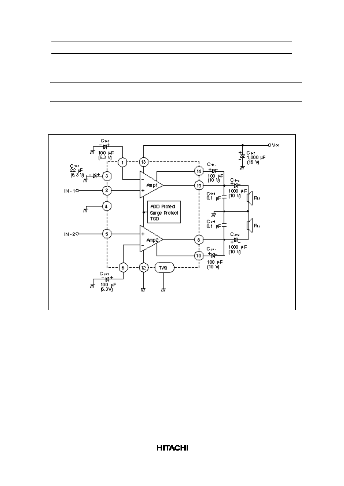
Block Diagram
Note: C
, C
must be non secondary resonance type (non inductive) polyester film capacitor for
104
204
keeping stability.
Figure 1 Typical Application Circuit
3
Page 4

HA13119
Figure 2 Voltage Gain vs. Frequency
Figure 3 Total Harmonic Distortion vs. Frequency
4
Page 5

Figure 4 Output Power vs. Frequency
HA13119
Figure 5 Cross-talk vs. Frequency
5
Page 6

HA13119
Figure 6 Supply Voltage Rejection Ratio vs. Frequency
Figure 7 Output Power vs. Supply Voltage
6
Page 7

Figure 8 Noise Output vs. Signal Source Resistance
HA13119
Figure 9 Total Harmonic Distortion vs. Output Power
7
Page 8

HA13119
Figure 10 Power Dissipation vs. Output Power
8
Page 9

HA13119
When using this document, keep the following in mind:
1. This document may, wholly or partially, be subject to change without notice.
2. All rights are reserved: No one is permitted to reproduce or duplicate, in any form, the whole or
part of this document without Hitachi’s permission.
3. Hitachi will not be held responsible for any damage to the user that may result from accidents or
any other reasons during operation of the user’s unit according to this document.
4. Circuitry and other examples described herein are meant merely to indicate the characteristics and
performance of Hitachi’s semiconductor products. Hitachi assumes no responsibility for any
intellectual property claims or other problems that may result from applications based on the
examples described herein.
5. No license is granted by implication or otherwise under any patents or other rights of any third party
or Hitachi, Ltd.
6. MEDICAL APPLICATIONS: Hitachi’s products are not authorized for use in MEDICAL
APPLICATIONS without the written consent of the appropriate officer of Hitachi’s sales company.
Such use includes, but is not limited to, use in life support systems. Buyers of Hitachi’s products
are requested to notify the relevant Hitachi sales offices when planning to use the products in
MEDICAL APPLICATIONS.
9
 Loading...