

Page 1
HA13118
18 W BTL Audio Power Amplifier
ADE-207-329 (Z)
1st Edition
Dec. 2000
Description
The HA13118 is power IC designed for component car stereo amplifiers. At 13.2 V to 4 Ω load, this power
IC provides an output power of 18W with 10% distortion.
It is easy to design as this IC employs internal each protection circuit and the new small package.
Features
• Small outline package, easy to mount
• Internal each protection circuits
Surge protection circuit
Thermal shut-down circuit
Ground fault protection circuit
Power supply fault protection circuit
Absolute Maximum Ratings (Ta = 25°C)
Item Symbol Rating Unit Note
Operating supply voltage V
DC supply voltage VCC (DC) 26 V 1
Peak supply voltage VCC (peak) 50 V 2
Output current Io (peak) 4 A
Power dissipation P
Thermal resistance θj – c 3.5 °C/W
Junction temperature Tj 150 °C
Operating temperature Topr –30 to +80 °C
Storage temperature Tstg –55 to +125 °C
Notes: 1. Value at t = 30 sec.
2. Value at width tw = 200 ms and rise time tr = 1 ms.
CC
T
18 V
15 W
Page 2
HA13118
Electrical Characteristics (VCC = 13.2 V, f = 1 kHz, RL = 4 Ω, Ta = 25 °C)
Item Symbol Min Typ Max Unit Test Conditions
Quiescent current I
Input bias voltage V
Output offset voltage ∆V
Voltage gain G
Q
B
Q
V
Output power Pout 15 18 — W THD = 10 % RL = 4 Ω
Total harmonic distortion THD — 0.2 1.0 % Pout = 1.5 W
Output noise voltage WBN — 1.0 2.0 mV Rg = 10 kΩ, BW = 20 Hz
Supply voltage rejection
SVR 33 44 — dB f = 500 Hz
ratio
Input resistance Rin 20 30 40 kΩ
Rolloff frequency f
L
f
H
40 80 160 mA Vin = 0
—2040mVVin = 0
— — +330 mV Vin = 0
53 55 57 dB Vin = –55 dBm
—11— R
= 8 Ω
L
20 kHz
—20—Hz∆Gv = –3 dB Low
10 20 40 kHz from f = 1 kHz Ref. High
Rev.1, Dec. 2000, page 2 of 8
Page 3
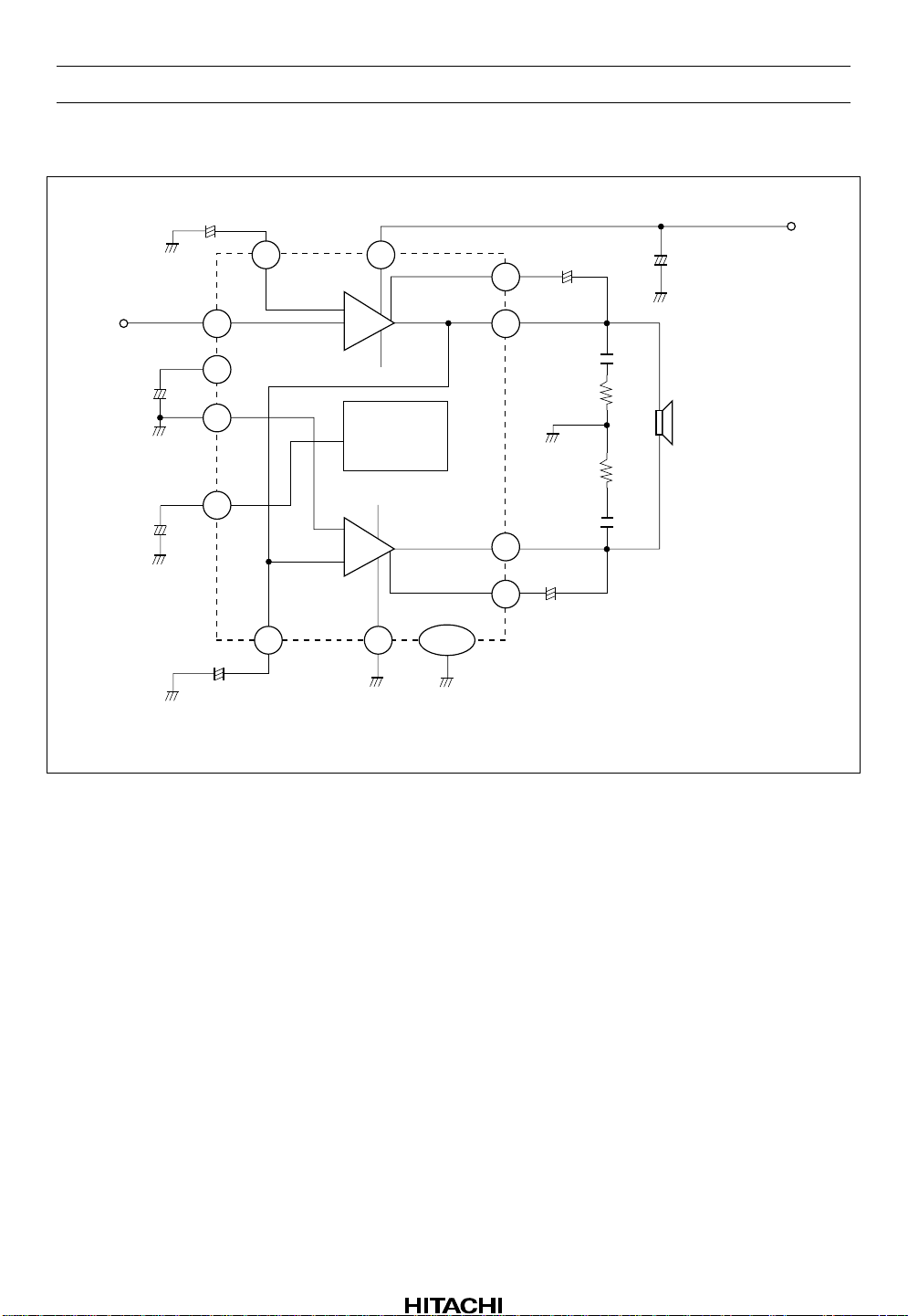
Block Diagram
C
100 (6.3 V)
Input
C
103
+
µ
100 F
(6.3 V)
C
10
(6.3 V)
Note: C
104
µ
105
stability.
–
+
–
, C
must be non secondary resonance type (non inductive) polyester film capacitor for keeping
106
101
µ
+
–
3
2
4
5
+
–
C
102
µ
100 (6.3V)
HA13118
V
C
14
108
100 (10 V)
µ
+
–
131
+
C
107
2,200
(16 V)
µ
–
–
Amp1
+
ASO Protect
Surge Protect
TSD
+
Amp2
15
C
105
µ
0.1
R
101
2.2
R
2.2
C
0.1
102
106
µ
R
L
4 - 8
Ω Ω
8
–
10
+
–
C
109
µ
6
12
TAB
100
(10 V)
CC
Figure 1 Typical Application Circuit
Rev.1, Dec. 2000, page 3 of 8
Page 4

HA13118
R = 4
L
Ω
out
30
f = 1 kHz
20
10
Output power P (W)
0
810121416
Supply voltage V (V)
18
CC
Figure 2 Output Power vs. Supply Voltage
60
V = 13.2 V
CC
R = 4
L
Ω
55
Gv (dB)
50
10
5020 100200 500 1 k 2 k 5 k 10 k20 k 50 k
Frequency f (Hz)
Figure 3 Voltage Gain vs. Frequency
100 k
Rev.1, Dec. 2000, page 4 of 8
Page 5

10
1.0
HA13118
V = 13.2 V
5
2
CC
L
R = 4
Ω
0.5
out
P = 8 W
0.2
0.1
out
P = 15 W
0.05
Total Harmonic Distortion THD (%)
0.02
20 50 100 200 500 1 k 2 k 5 k 10 k 20 k 50 k
Frequency f (Hz)
Figure 4 Total Harmonic Distortion vs. Frequency
10
5
V = 13.2 V
CC
Ω
R = 4
L
2
1.0
0.5
0.2
0.1
0.05
Total Harmonic Distortion THD (%)
f = 10 kHz
1 kHz
100 Hz
0.02
0.02
0.05 0.1 0.2 0.5 1.0 2 5 10 20
Output Power P (W)
out
Figure 5 Total Harmonic Distortion vs. Output Power
Rev.1, Dec. 2000, page 5 of 8
Page 6

HA13118
2.0
V = 13.2 V
CC
R = 4
L
1.0
0.5
0.2
0.1
Noise output WBN (mV)
0.05
Ω
0.02
1 k500 2 k 5 k 1 k 20 k 50 k
Signal source resistance R ( )gΩ
Figure 6 Noise Output vs. Signal Source Resistance
60
R = 4
L
Ω
V = 13.2 V
50
40
30
20
10
Supply voltage rejection ration SVR (dB)
0
20 50 100 200 500
Frequency f (Hz)
1 k
CC
V = 0 dB
ripple
5 k 10 k
2 k
20 k
Figure 7 Supply Voltage Rejection Ratio v s. Frequency
Rev.1, Dec. 2000, page 6 of 8
Page 7

Package Dimensions
HA13118
3.0 ± 0.2
11.3 ± 0.3
1.11 ± 0.25
1
19.66
20.5 Max
19.0 ± 0.3
1.27
2.54±0.25
φ
3.6 ± 0.2
7.8
15
0.6 ± 0.1
13.8
Hitachi Code
JEDEC
EIAJ
Mass
3.8 Max
1.5 Max
1.80 ± 0.25
+ 0.10
0.25
– 0.05
3.5 ± 0.5
6.04 ± 0.50
(reference value)
Unit: mm
17.90
SP-15TA
—
—
3.10 g
Rev.1, Dec. 2000, page 7 of 8
Page 8

HA13118
Disclaimer
1. Hitachi neither warrants nor grants licenses of any rights of Hitachi’s or any third party’s patent,
copyright, trademark, or other intellectual property rights for information contained in this document.
Hitachi bears no responsibility for problems that may arise with third party’s rights, including
intellectual property rights, in connection with u se of the information contained in this document.
2. Products and product specifications may be subject to change without notice. Confirm that you have
received the latest product standards or specifications before final design, purchase or use.
3. Hitachi makes every attempt to ensure that its products are of high quality and reliability. However,
contact Hitachi’s sales office before using the product in an application that demands especially high
quality and reliability or where its failure or malfunction may directly threaten human life or cause risk
of bodily injury, such as aerospace, aeronautics, nuclear power, combustion control, transportation,
traffic, safety equipment or medical equipment for life support.
4. Design your application so that the product is used within the ranges guaranteed by Hitachi particularly
for maximum rating, operating supply voltage range, heat radiation characteristics, installation
conditions and other characteristics. Hitachi bears no responsibility for failure or damage when used
beyond the guaranteed ranges. Even within the guaranteed ranges, consider normally foreseeable
failure rates or failure modes in semiconductor devices and employ systemic measures such as failsafes, so that the equipment incorporating Hitachi product does not cause bodily injury, fire or other
consequential damage due to operation of the Hitachi product.
5. This product is not designed to be radiation resistant.
6. No one is permitted to reproduce or duplicate, in any form, the whole or part of this document without
written approval from Hitachi.
7. Contact Hitachi’s sales office for any questions regarding this document or Hitachi semiconductor
products.
Sales Offices
Hitachi, Ltd.
Semiconductor & Integrated Circuits.
Nippon Bldg., 2-6-2, Ohte-machi, Chiyoda-ku, Tokyo 100-0004, Japan
Tel: Tokyo (03) 3270-2111 Fax: (03) 3270-5109
URL NorthAmerica : http://semiconductor.hitachi.com/
For further information write to:
Hitachi Semiconductor
(America) Inc.
179 East Tasman Drive,
San Jose,CA 95134
Tel: <1> (408) 433-1990
Fax: <1>(408) 433-0223
Europe : http://www.hitachi-eu.com/hel/ecg
Asia : http://sicapac.hitachi-asia.com
Japan : http://www.hitachi.co.jp/Sicd/indx.htm
Hitachi Europe GmbH
Electronic Components Group
Dornacher Straße 3
D-85622 Feldkirchen, Munich
Germany
Tel: <49> (89) 9 9180-0
Fax: <49> (89) 9 29 30 00
Hitachi Europe Ltd.
Electronic Components Group.
Whitebrook Park
Lower Cookham Road
Maidenhead
Berkshire SL6 8YA, United Kingdom
Tel: <44> (1628) 585000
Fax: <44> (1628) 585160
Hitachi Asia Ltd.
Hitachi Tower
16 Collyer Quay #20-00,
Singapore 049318
Tel : <65>-538-6533/538-8577
Fax : <65>-538-6933/538-3877
URL : http://www.hitachi.com.sg
Hitachi Asia Ltd.
(Taipei Branch Office)
4/F, No. 167, Tun Hwa North Road,
Hung-Kuo Building,
Taipei (105), Taiwan
Tel : <886>-(2)-2718-3666
Fax : <886>-(2)-2718-8180
Telex : 23222 HAS-TP
URL : http://www.hitachi.com.tw
Hitachi Asia (Hong Kong) Ltd.
Group III (Electronic Components)
7/F., North Tower,
World Finance Centre,
Harbour City, Canton Road
Tsim Sha Tsui, Kowloon,
Hong Kong
Tel : <852>-(2)-735-9218
Fax : <852>-(2)-730-0281
URL : http://www.hitachi.com.hk
Copyright Hitachi, Ltd., 2000. All rights reserved. Printed in Japan.
Colophon 2.0
Rev.1, Dec. 2000, page 8 of 8
 Loading...