

Page 1

HA12226F/HA12227F
Audio Signal Processor for Cassette Deck
(Dolby B-type NR with Recording System)
ADE-207-270E (Z)
6th Edition
Dec. 2000
Description
The HA12226F/HA12227F are silicon monolithic bipolar IC providing Dolby noise reduction system*1,
music sensor system, REC equalizer system and each electronic control switch in one chip.
Note: 1. Dolby is a trademark of Dolby Laboratories Licensing Corporation.
A license from Dolby Laboratories Licensing Co r por ation is required for the use of this IC.
The HA12227F is not built-in Dolby B-NR.
Functions
• Dolby B-NR*2× 2 channel
• REC equalizer × 2 channel
• Music sensor × 1 channel
• Pass amp. × 2 channel
• Each electronic control switch to change REC equalizer, bias, etc.
Note: 2. The HA12227F is not built-in Dolby B-NR.
Features
• REC equalizer is very small number of external parts and have 4 types of frequency characteristics
built-in.
• 2 types of input for PB, 1 type of input for REC.
• 70µ - PB equalizer changing system built-in.
• Dolb y NR*
Unprocessed signal output available from recording out terminals during PB mode.
• Provide stable music sensor system, available to design music sensing time and level.
• Controllable from direct micro-computer output.
• Bias oscillator control switch built-in.
• NR ON / OF F and REC / PB fully electronic control switch ing built-in.
• Normal-speed / high-speed, Normal / Crom and PB equalizer fully electronic control switching built-in.
• Available to reduce substrate-area because of high integration and small external parts.
2
with dubbing double cassette decks.
Page 2

HA12226F/HA12227F
Ordering Information
Operating Voltage
Product Power Supply Range (Single Supply)
HA12226F 11.0 V to 15.0 V
HA12227F
Standard Level
Product Package PB-OUT Level REC-OUT Level Dolby Level
HA12226F FP-56A 580 mVrms 300 mVrms 300 mVrms
HA12227F
Function
9.5 V to 15.0 V
Music
Product Dolby B-NR REC-EQ
HA12226F ❍❍❍❍❍❍
HA12227F × ❍❍❍❍❍
Note: Depending on the employed REC / PB head and test tape characteristics, there is a rare case that
the REC-EQ characteristics of this LSI can not be matched to the required characteristics because of
built-in resistors which determined the REC-EQ parameters in this case, please inquire the
responsible agent because the adjustment built-in resistor is necessary.
Sensor Pass Amp.
REC / PB
Selection ALC
Difference of HA12215F and HA12226F/HA12227F
Tape Correspondence
Product Supply Voltage NORM CROM METAL
HA12226F/HA12227F Single supply voltage ❍❍×
HA12215F Split supply voltage ❍❍❍
Note: The HA12226F/HA12227F became single power supply for the HA12215F and deleted metal
correspondence. The HA12227F is not built-in Dolby B-NR.
Other characteristic aspects are similar as the HA12215F.
Rev.6, Dec. 2000, page 2 of 86
Page 3
HA12226F/HA12227F
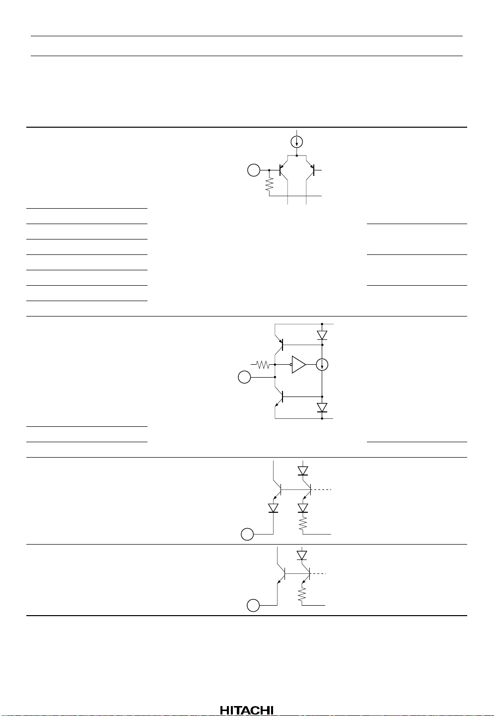
Pin Description, Equivalent Circuit (VCC = 12 V, A system of single supply voltage,
Ta = 25°C, No Signal, The value in the show typical value.)
Pin No. Terminal Name Note Equivalent Circuit Pin Description
51 AIN (R) V = V
/ 2
CC
V
100k
VCC/2
48 AIN (L)
53 BIN (R) PB B Deck input
46 BIN (L)
56 RIN (R) REC input
43 RIN (L)
5 EQIN (R) REC equalizer input
38 EQIN (L)
2
1 *
DET (R) V = 2.7 V
V
CC
PB A Deck input
Time constant pin for
Dolby-NR
V
GND
2
42 *
DET (L)
49 RIP Ripple filter
3
2 *
BIAS1 V = 0.6 V
Dolby bias current
input
V
41 BIAS2 V = 1.3 V
GND
REC equalizer bias
current input
V
GND
Rev.6, Dec. 2000, page 3 of 86
Page 4
HA12226F/HA12227F
Pin Description, Equivalent Circuit (VCC = 12 V, A system of single supply voltage,
Ta = 25°C, No Signal, The value in the show typical value.) (cont)
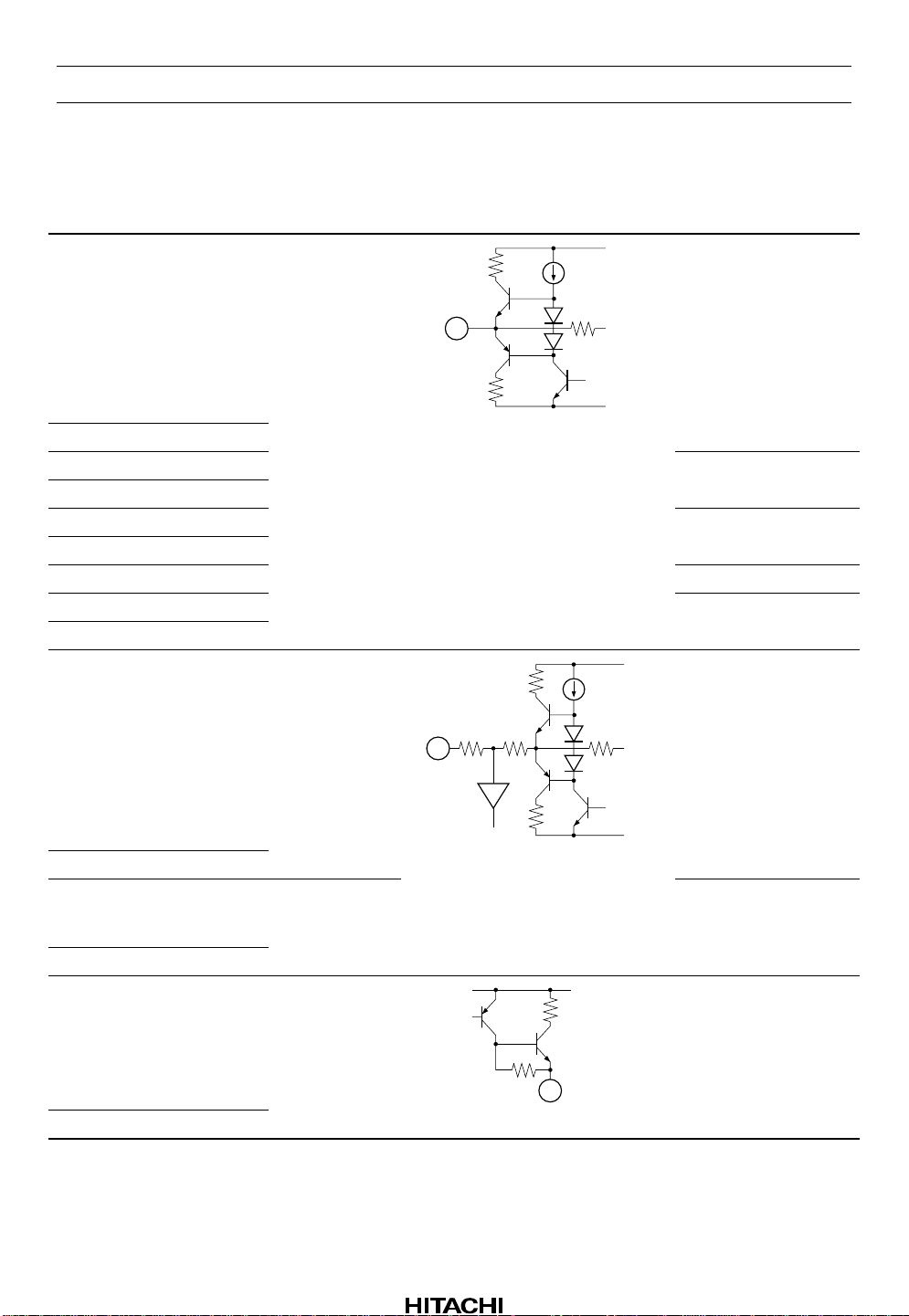
Pin No. Terminal Name Note Equivalent Circuit Pin Description
3 PBOUT (R) V = V
/ 2
CC
V
CC
V
GND
40 PBOUT (L)
4 RECOUT (R) REC output
39 RECOUT (L)
7 EQOUT (R) REC equalizer output
36 EQOUT (L)
28 MAOUT MS Amp. output *
8 ROUT (R) Input Amp. output
35 ROUT (L)
52 ABO (R) R1 = 15 k
V
R2 = 12 k
V = VCC / 2
R2R1
V
PB output
Time constant pin for
CC
PB equalizer (70µ)
1
47 ABO (L)
6 BOOST (R) R1 = 4.8 k
R2 = 4.8 k
V = VCC / 2
37 BOOST (L)
32 BIAS (C) V = VCC − 0.7 V
33 BIAS (N)
Rev.6, Dec. 2000, page 4 of 86
GND
Time constant pin for
low boost
V
CC
REC bias current
output
V
Page 5
HA12226F/HA12227F
Pin Description, Equivalent Circuit (VCC = 12 V, A system of single supply voltage,
Ta = 25°C, No Signal, The value in the show typical value.) (cont)
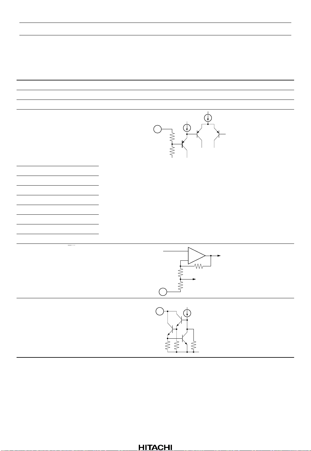
Pin No. Terminal Name Note Equivalent Circuit Pin Description
21 V
CC
V = V
CC
50 GND V = 0 V GND pin
31, 45, 54 NC No connection No connection
15 ALC ON/OFF I = 20 µA
Power supply
Mode control input
16 PB A/B
17 A 120/70
18 NORM/HIGH
19 B NORM/CROM
20 BIAS ON/OFF
22 RM ON/OFF
2
23 *
NR ON/OFF
25 LM ON/OFF
24 REC/PB/PASS
26 MSOUT I = 0 µA
V
22 k
100 k
V
V
GND
2.5 V
100 k
22 k
I
+
Mode control input
−
100 k
V
CC
MS output (to MPU) *
1
I
D GND
Rev.6, Dec. 2000, page 5 of 86
Page 6
HA12226F/HA12227F
Pin Description, Equivalent Circuit (VCC = 12 V, A system of single supply voltage,
Ta = 25°C, No Signal, The value in the show typical value.) (cont)
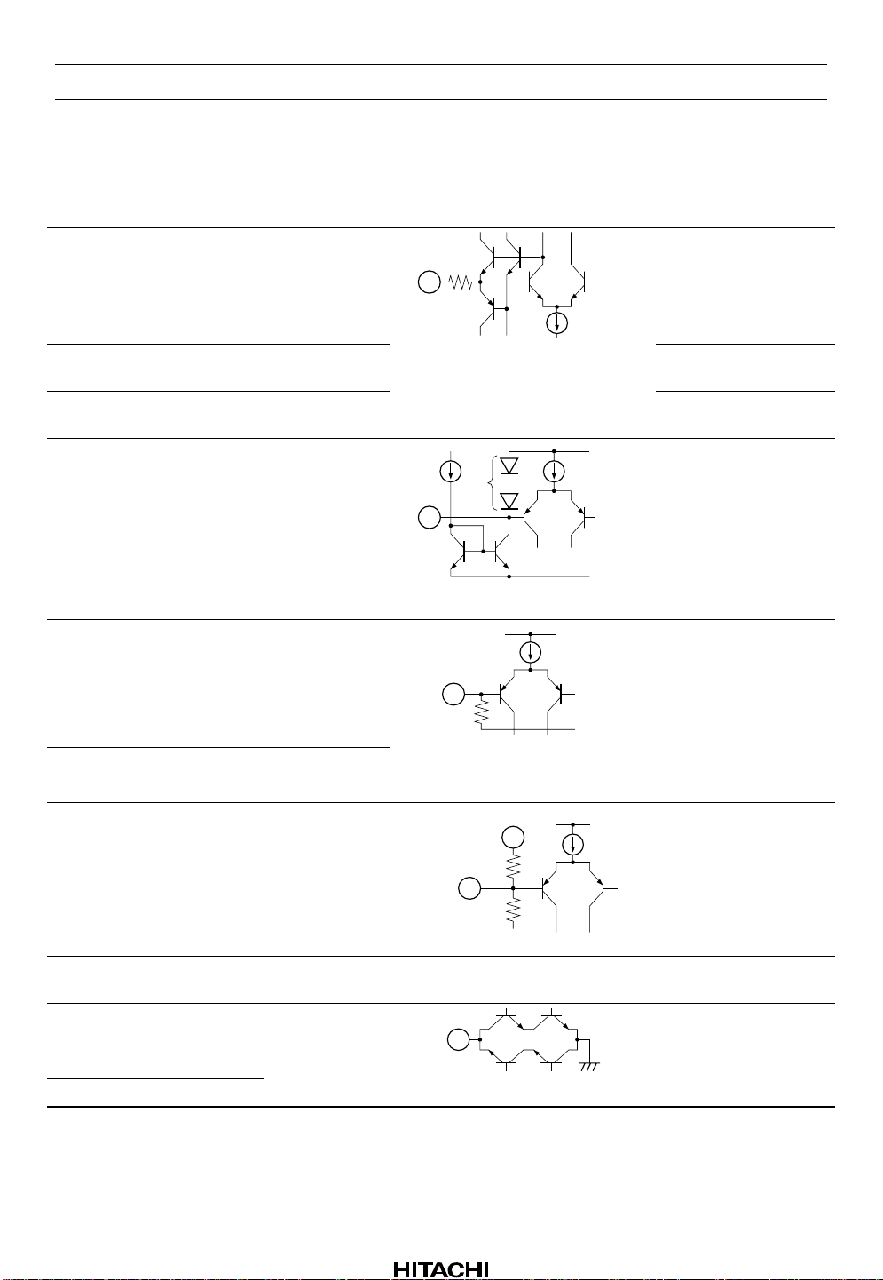
Pin No. Terminal Name Note Equivalent Circuit Pin Description
10 GPCAL R = 110 kΩ
R
2.5 V
11 RECCAL R = 110 kΩ REC gain calibration
12 ALCCAL R = 140 kΩ ALC operation level
14 MSDET n = 6
0 µA
V
CC
n
GND
13 ALCDET n = 2
27 MSIN R = 50 kΩ
V
CC
GP gain calibration
terminal
terminal
calibration terminal
Time constant pin for
1
MS *
MS input *
1
V
R
VCC/2
9 ALCIN (R) R = 100 kΩ
34 ALCIN (L)
30 MAI V = VCC / 2
MAOUT
V
CC
MS Amp. input *
1
100 k
V
MAI
8.2 k
VCC/2
29 MS GND V = 0 V MS output voltage
level control pin *
1
55 ALC (R) V = 0 V Variable impedance
for attenuation
44 ALC (L)
Note: 1. MS: Music Sensor
2. Non connection regarding the HA12227F.
3. Test pin regarding the HA12227F.
Rev.6, Dec. 2000, page 6 of 86
Page 7
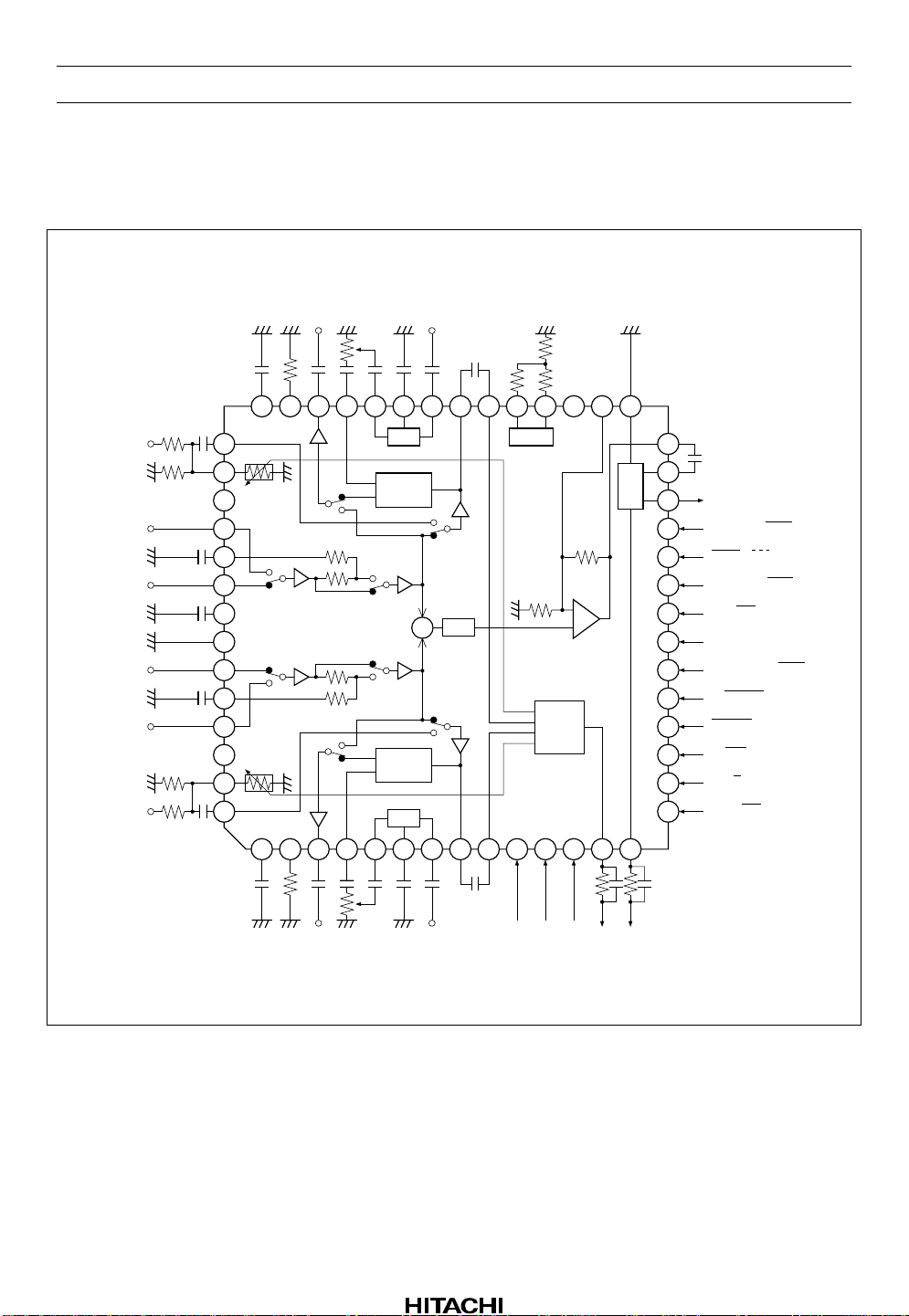
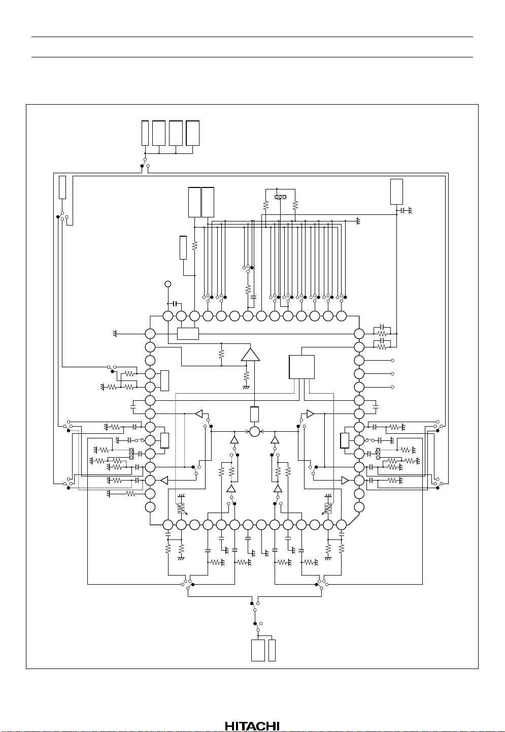
Block Diagram
HA12226F
DET (L)
BIAS2
42 41 39 38 37 36 35 34 33 32 31 30 2940
PBOUT (L)
RECOUT (L)
EQIN (L)
BOOST (L)
EQOUT (L)
ROUT (L)
ALCIN (L)
BIAS (N)
BIAS (C)
NC
HA12226F/HA12227F
MAI
MSGND
RIN (L)
ALC (L)
BIN (L)
ABO (L)
AIN (L)
RIP
GND
AIN (R)
ABO (R)
BIN (R)
ALC (R)
RIN (R)
43
44
45NC
46
47
48
49
50
51
52
53
54NC
55
56
1 2 3 4 5 6 7 8 9 10 11 12 13 14
BIAS1
DET (R)
PBOUT (R)
EQ
Dolby
B-NR
Dolby
B-NR
EQ
EQIN (R)
RECOUT (R)
BOOST (R)
+
LPF
EQOUT (R)
ROUT (R)
ALCIN (R)
BIAS
GPCAL
−
+
ALC
ALCCAL
RECCAL
MS
MSDET
ALCDET
28
27
26
25
24
23
22
21
20
19
18
17
16
15
MAOUT
MSIN
MSOUT
LM ON / OFF
REC / PB / PASS
NR ON / OFF
RM ON / OFF
V
CC
BIAS ON / OFF
B NORM / CROM
NORM / HIGH
A 120 / 70
PB A / B
ALC ON / OFF
Rev.6, Dec. 2000, page 7 of 86
Page 8
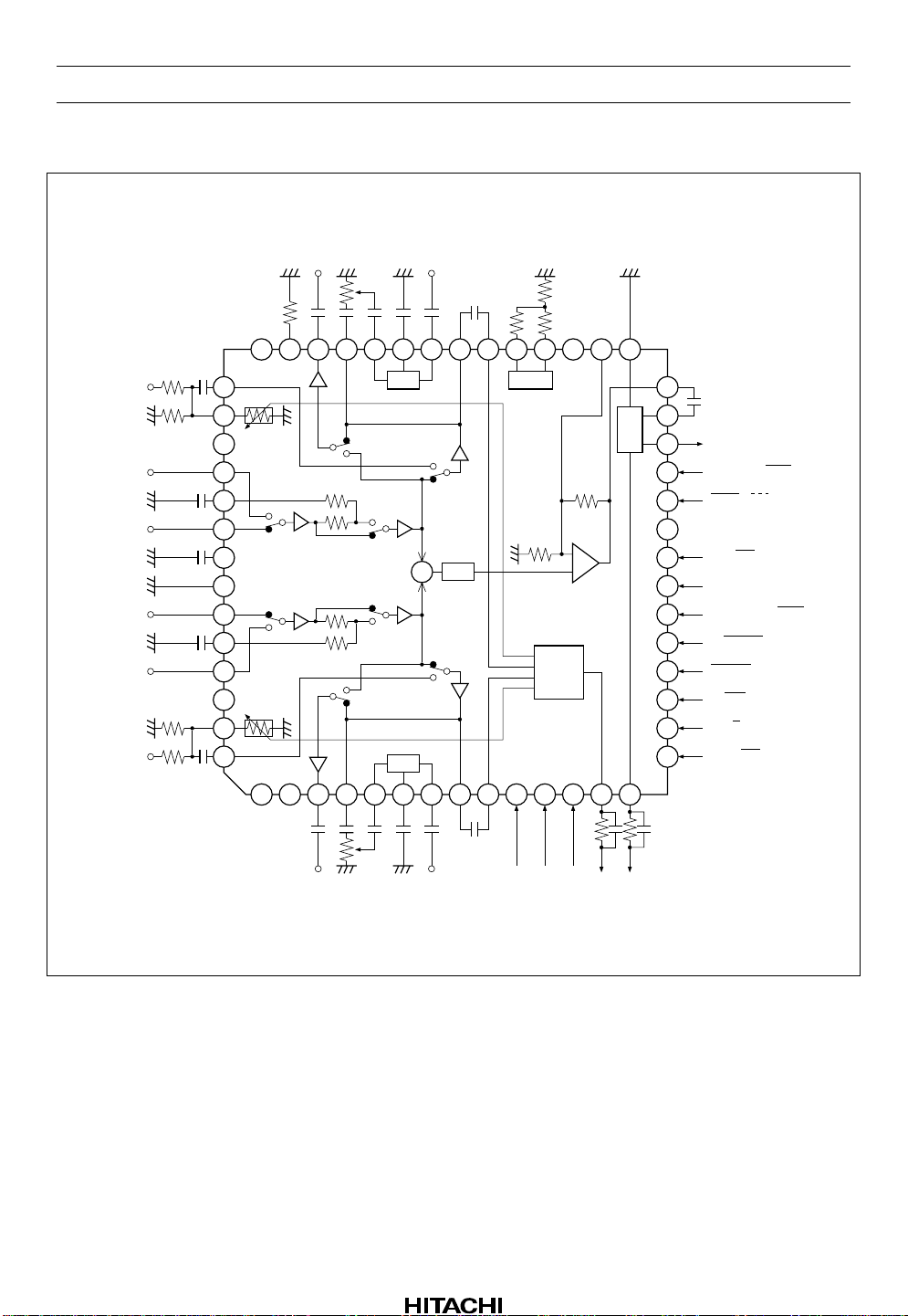
HA12226F/HA12227F
HA12227F
NC
42 41 39 38 37 36 35 34 33 32 31 30 2940
BIAS2
PBOUT (L)
RECOUT (L)
EQIN (L)
BOOST (L)
EQOUT (L)
ROUT (L)
ALCIN (L)
BIAS (N)
BIAS (C)
NC
MAI
MSGND
RIN (L)
ALC (L)
BIN (L)
ABO (L)
AIN (L)
RIP
GND
AIN (R)
ABO (R)
BIN (R)
ALC (R)
RIN (R)
43
44
45NC
46
47
48
49
50
51
52
53
54NC
55
56
1 2 3 4 5 6 7 8 9 10 11 12 13 14
NC
PBOUT (R)
Test mode pin
EQ
EQ
EQIN (R)
RECOUT (R)
BOOST (R)
+
LPF
EQOUT (R)
ROUT (R)
ALCIN (R)
BIAS
GPCAL
−
+
ALC
ALCCAL
RECCAL
MS
MSDET
ALCDET
28
27
26
25
24
23
22
21
20
19
18
17
16
15
MAOUT
MSIN
MSOUT
LM ON / OFF
REC / PB / PASS
NC
RM ON / OFF
V
CC
BIAS ON / OFF
B NORM / CROM
NORM / HIGH
A 120 / 70
PB A / B
ALC ON / OFF
Rev.6, Dec. 2000, page 8 of 86
Page 9

HA12226F/HA12227F
Parallel-Data Format
MODE
Pin No. Pin Name Lo Mid Hi
15 ALC ON/OFF ALC ON ALC OFF Lo
16 PB A/B Ain *
1
Bin *
1
17 A 120/70 *1 *1 Lo
22 RM ON/OFF REC MUTE ON REC MUTE OFF Lo
20 BIAS ON/OFF BIAS OFF BIAS ON Lo
2
23 *
NR ON/OFF NR OFF NR ON Lo
24 REC/PB/PASS REC MODE PB MODE REC MODE PASS Mid
25 LM ON/OFF LINE MUTE OFF LINE MUTE ON Lo
18 NORM/HIGH Normal speed High speed Lo
19 B NORM/CROM REC EQ Normal *
Bias Normal
1
REC EQ CROM *
Bias CROM
1
REC EQ CROM *
Bias CROM
Note: 1. PB EQ logic
PB
A 120
120/70 B NORM
120120
NORM / CROM Lo Hi
NORM NORM
Lo Lo FLAT FLAT
Lo Mid or Hi FLAT 70 µ
Hi Lo 70 µ FLAT
Hi Mid or Hi 70 µ 70 µ
“Pin Open”
Lo
1
Lo
2. The HA12226F only.
Rev.6, Dec. 2000, page 9 of 86
Page 10
HA12226F/HA12227F
Functional Description
Power Supply Range
These ICs are designed to operate on single supply.
Table 1 Supply Voltage
Product Power Supply Range (Single Supply)
HA12226F 11.0 V to 15.0 V
HA12227F
Note: The lower limit of supply voltage depends on the line output reference level.
The minimum value of the overload margin is specified as 12 dB by Dolby Laboratories (Dolby IC
HA12226F).
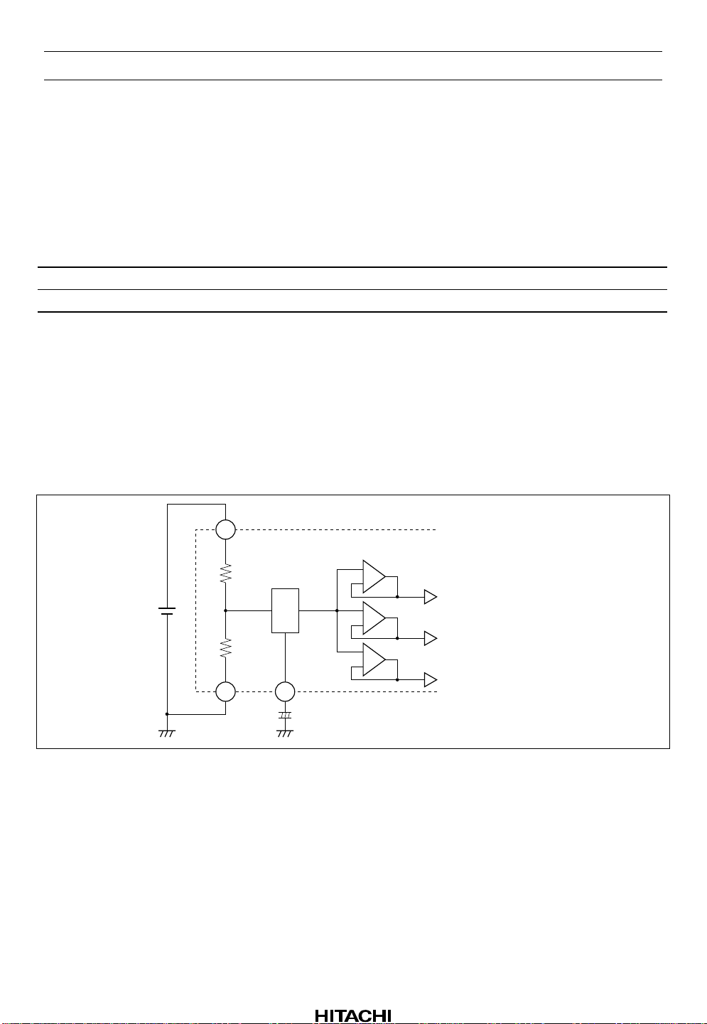
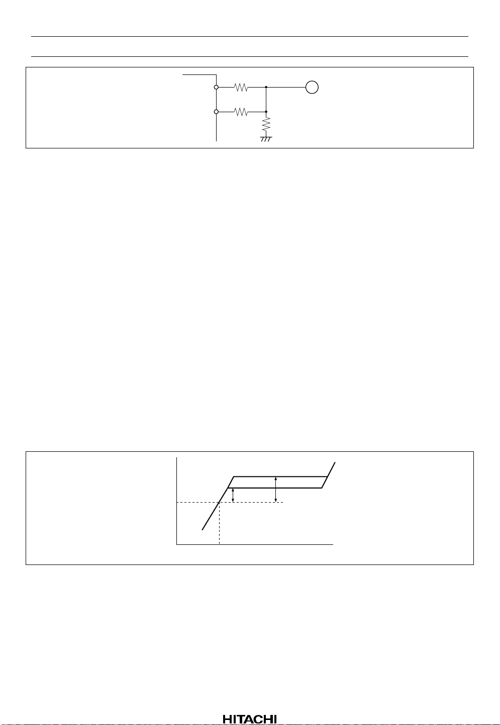
Reference Voltage
The reference voltage are provided for the left channel and the right channel separately. The block diagram
is shown as figure 1.
9.5 V to 15.0 V
V
CC
21
+
−
V
CC
50
GND
49
+
RIP
1µ
+
−
+
−
L channel reference
Music sensor reference
R channel reference
Unit C: F
Figure 1 Reference Voltage
Rev.6, Dec. 2000, page 10 of 86
Page 11
HA12226F/HA12227F
Operating Mode Control
The HA12226F/HA12227F provide fully electronic switching circuits. And each operating mode control is
controlled by parallel data (DC voltage).
Table 2 Control Voltage
Pin No. Lo Mid Hi Unit Test Condition
15, 16, 17, 18, 20,
4
22, 23*
, 25
−0.2 to 1.0 4.0 to V
CC
V
Input Pin Measure
19, 24 −0.2 to 1.0 2.0 to 3.0 4.0 to V
CC
Notes: 1. Each pins are on pulled down with 100 kΩ inter nal resi stor.
Therefore, it will be low-level when each pins are open.
But pin 24 is mid-level when it is open.
2. Over shoot level and under shoot level of input signal must be the standardized (High: V
Low: −0.2 V).
3. For reduction of pop noise, connect 1 µF to 22 µF capacitor with mode control pins.
But it is impossible to reduce completely in regard to Line mute, therefore, use external mute at
the same time.
4. Non connection regarding the HA12227F.
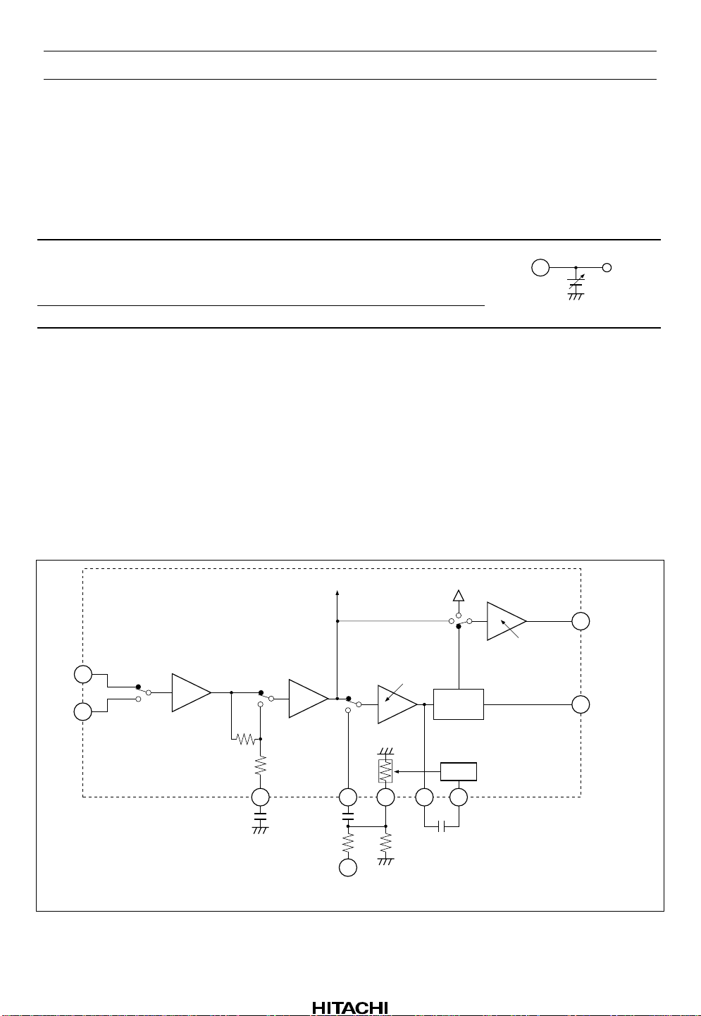
Input Block Diagram and Lev e l Diagram
The each level shown above is typical value
when offering PBOUT level to PBOUT pin.
R3
12k
C2
FLAT
(120µ)
70µs
R4
15k
25.5mVrms
200mVrms
AIN
BIN
Note: 1. The HA12227F is not built-in Dolby B-NR.
25.9mVrms
21.3dB
300mVrms
4700pF
MS REF
300mVrms
PB/REC,
PASS=0dB/21.4dB
C1
0.1µF
R1
15k
RIN
PB
REC
PASS
0dB
R2
2.2k
PASS
300mVrms
0.1µF
V
Dolby
B-NR
ALC
C3
REC
PB
PASS/REC,
PB=5.7dB/5.7dB
300mVrms
1
*
,
CC
PBOUT
580mVrms
RECOUT
300mVrms
Figure 2 Input Block Diagram
Rev.6, Dec. 2000, page 11 of 86
Page 12
HA12226F/HA12227F
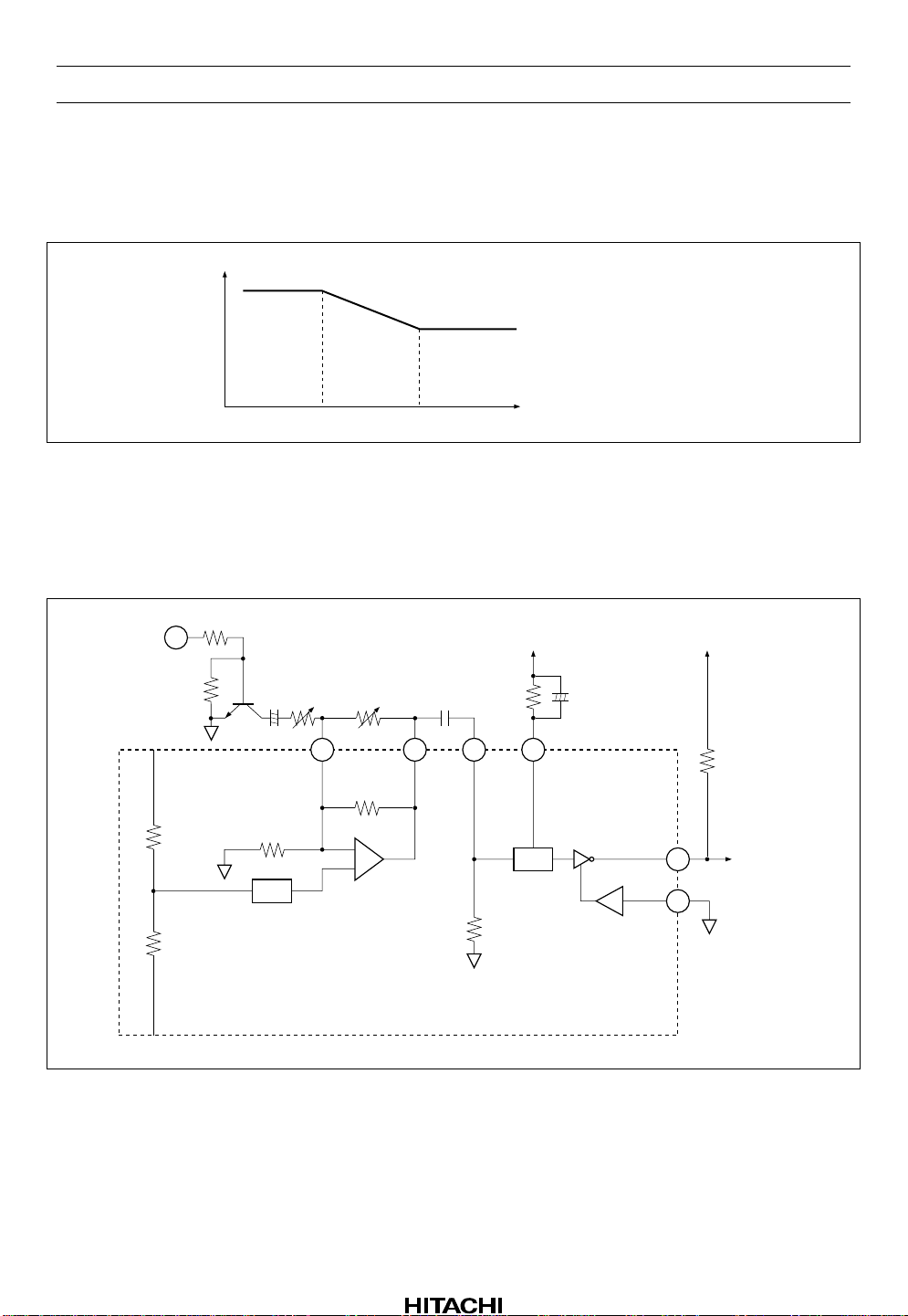
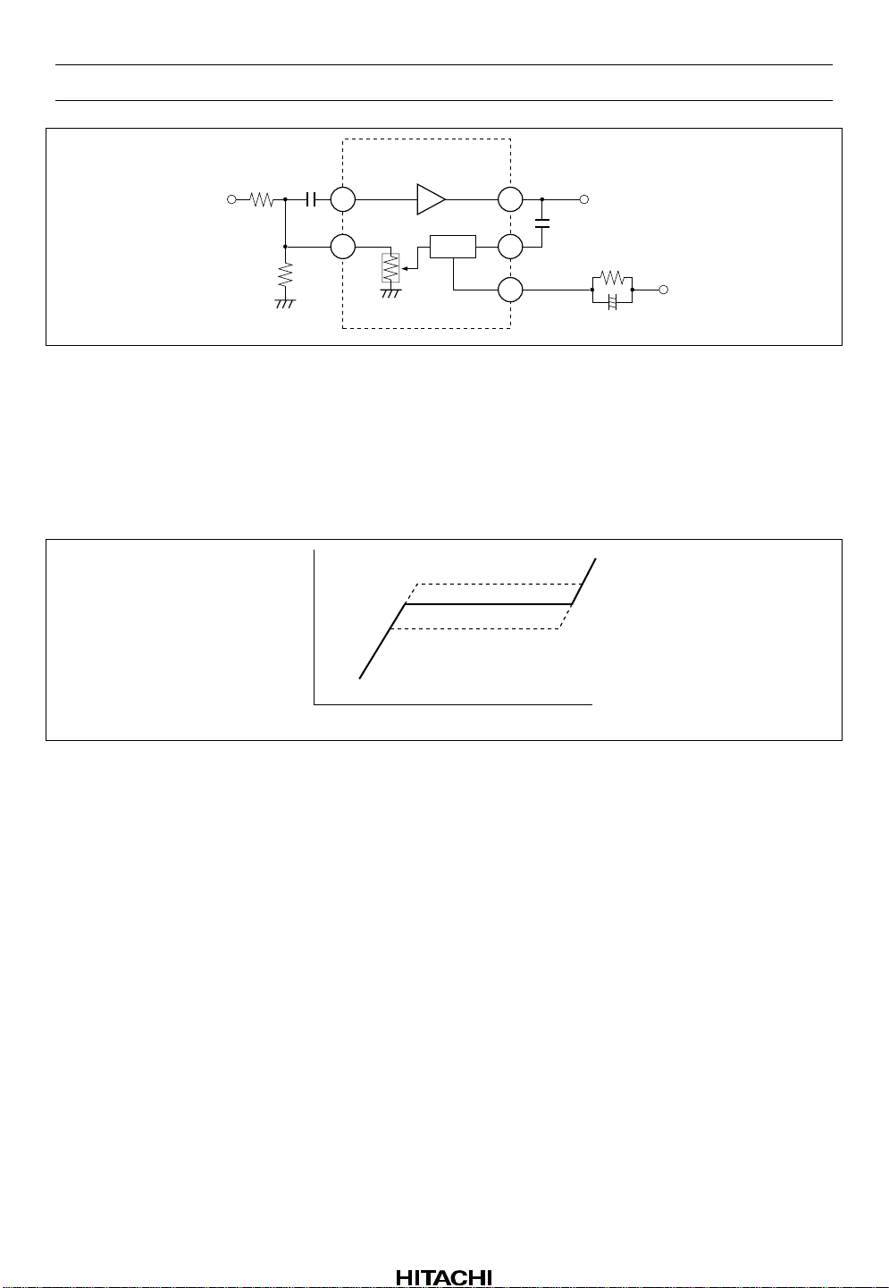
PB Equalizer
By switching logical input level of pin 17 (for Ain) and pin 19 (for Bin), you can equalize corresponding to
tape position at play back mode.
G
V
t1 = C2 ⋅ (12k + 15k)
t2 = C2 ⋅ 15k
t1 t2
Figure 3 Frequency Characteristic of PB Equalizer
The Sensitivity Adjustment o f Music Sensor
Adjusting MS Amp gain by external resistor , the sensitivity of music sensor can set up.
REP
f
V
CC
D V
CC
PB (L)
−6dB
PB (R)
8.2k
LPF
25kHz
C16
+
MAI
100k
−
+
1000p
MA
OUT
MS AMP
R13
330k
MSIN
50k
Figure 4 Music Sensor Block Diagram
DET
MS
DET
+
C13
0.33µ
MS OUT
GND
R
L
Microcomputer
GND
Rev.6, Dec. 2000, page 12 of 86
Page 13
HA12226F/HA12227F
The Sensitivity of Music Sensor
A standard level of MS input pin 25.9 mVrms, therefore, the sensitivity of music sensor (S) can request
it, by lower formulas.
A = MS Amp Gain*
B = PB input Gain × (1/2)*
C = Sensed voltage
20log (A × B) = D [dB]
C = 130 [mVrms] (Intenally voltage in a standard)
PB input Gain = 21.3 [dB]
Notes: 1. When there is not a regulation outside.
2. Case of one-sided channel input.
But necessary to consider the same attenuation quantity practically, on account of A(B) h ave made
frequency response.
37.7dB
1
2
S = 20log
S = 14 − D [dB]
G
V
C
25.9 ⋅ A ⋅ B
[dB]
f1 =
f2 = 25k [Hz]
f
f1 f2
1
2π ⋅ C16 ⋅ 50k
[Hz]
Figure 5 Frequency Characteristic of MSIN
Occasion of the external component of figure 4, f1 is 3.18 kHz.
Time constant of detection
Figure 6(1) generally shows that detection time is in proportion to value of capacitor C13. But, with
Attack*
2
and Recovery*3 the detection time differs exceptionally.
Notes 2. Attack : Non-music to Music
3. Recovery : Music to Non-music
Recovery
Attack
Detection time
C13
(1) (2) (3)
Recovery Recovery
Attack Attack
Detection time
R13
Detection level
Detection time
Input level
Figure 6 Function Characteristic of MS
Like the figure 6(2), Recovery time is variably possible by value of resistor R13. But Attack time gets
about fixed value. Attack time has dependence by input level. When a large signal is inputted, Attack time
is short tendency.
Rev.6, Dec. 2000, page 13 of 86
Page 14
HA12226F/HA12227F
Music Sensor Output (MSOUT)
As for internal circuit of music sensor block, music sensor output pin is connected to the collector of
NPN type directly, output level will be “high” when sensing no signal. And output level will be “low”
when sensing signal.
Connection with microcomputer, it is requested to use external pull up resistor (R
Note: Supply voltage of MSOUT pin must be less than V
voltage.
CC
= 10 kΩ to 22 kΩ)
L
The Tolerances of External Components for Dolby NR-Block
(Only the HA12226F)
For Dolby NR precision securing, please use external components shown at figure 7. If leak-current are a
few electrolytic-capacitor, it can be applicable to C5 and C23.
C23
0.1µ
±10%
42
DET (L)
HA12226F
DET (R)
C5
0.1µ
±10%
BIAS1
1
2
R5
33k
±2%
Figure 7 Tolerance of External Components
Low-Boost
EQIN
24.6dB
4.8k
4.8k
BOOST
+
C9(C19)
0.47µ
REC EQ
EQOUT
Figure 8 Example of Low Boost Circuit
External components shown figure 8 gives frequency response to take 6 dB boost. And cut off frequency
can request it, by C9 (C19).
Rev.6, Dec. 2000, page 14 of 86
Page 15
HA12226F/HA12227F
REC Equalizer
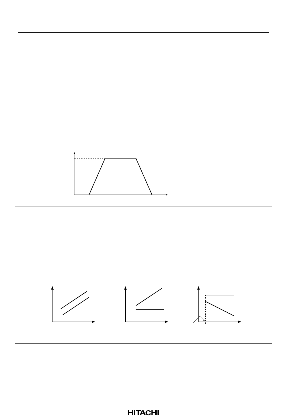
The outlines of REC Equalizing frequency characteristics are sh own by figure 9. Those peak level can be
set up by supplying voltage. (0 V to 5 V, GND = 0 V) to pin 10 (GPCAL).
And whole band gain can be set up by supplying voltage (0 V to 5 V, GND = 0 V) to pin 11 (RECCAL).
Both setting up range are ±4.5 dB. In case that you do not need setting up, pin 10, pin 11 should be open
bias.
Note: Depending on the employed REC/PB head and test tape characteristics, there is a rare case that the
REC-EQ characteristics of this LSI can not be matched to the required characteristics because of
built-in resistors which determined the REC-EQ parameters in this care, please inquire the
responsible agent because of the adjustment of built-in resistor is necessary.
RECCAL
GPCAL
Gain (dB)
Frequency (Hz)
Figure 9 Frequency Characteristics of REC Equalizer
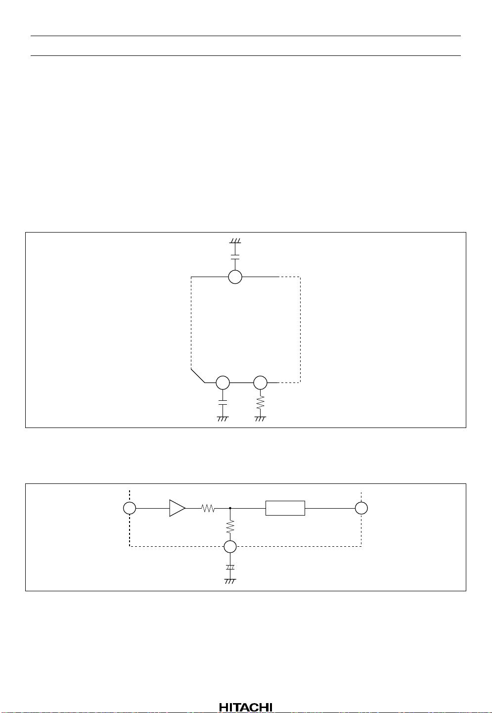
Bias Switch
The HA12215F built-in DC voltage generato r for bias oscillator and its bias switches.
External resistor R20, R21 which corresponded with tape positions and bias out voltage are relater with
below.
.
Vbias = × (VCC − 0.7) [V]
.
(R20 or R21) + R22
R22
Bias switch follows to a logic of pin 19 (B / Nor m / Crom).
Note: A current that flows at bias out pin, please use it less than 5 mA.
Rev.6, Dec. 2000, page 15 of 86
Page 16
HA12226F/HA12227F
BIAS (N)
Pin 33
BIAS (C)
Pin 32
R21
R20
Vbias
R22
Figure 10 External Components of Bias Block
Automatic Level Control
ALC is the input decay rate variable system. It has internal variable resistors of pin 55 (pin 44) by
RECOUT signal that is inputted to p in 9 (pin 34 ) .
The operation is similitude to MS, detected by pin 13.
The signal input pin is pin 56 (pin 43). Resistor R1, R2 and capacitor C2, external components, for the
input circuit are commended as figure 12. There are requested to use value of the block diagram figure for
performance maintenance of S/N, T.H.D. etc.
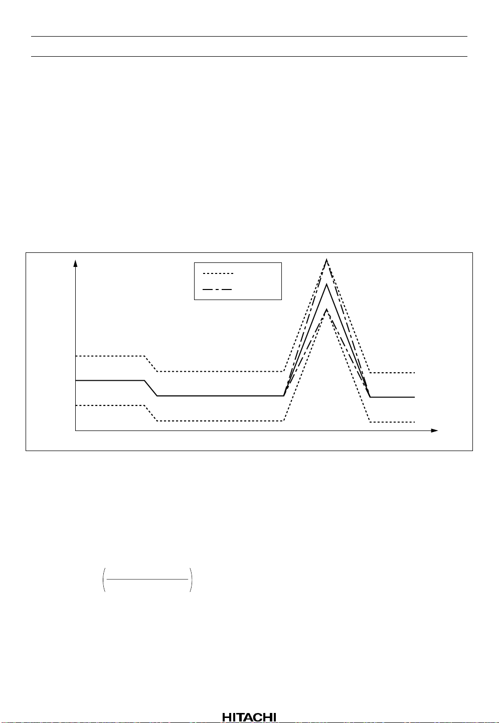
Figure 11 shows the relation with R1 front RIN point and ROUT.
ALC operation level acts for the center of +4.5 dB at tape position TYPE I and the center of +2.5 dB at tape
position TYPE II, to standard level (300 mVrms).
Then, adopted maximum value circuit, ALC is operated by a large channel of a signal.
ALC ON/OFF can switch it by pin 15. Please do ALC ON, after it does for one time ALC OFF inevitably,
for ALC time to start usefully (when switching PB → PASS, when switching PB → PASS), in order to
reset ALC circuit.
TYPE I
4.5dB
RIN
300mV
ROUT
TYPE II
2.5dB
Figure 11 ALC Operation Level
Rev.6, Dec. 2000, page 16 of 86
Page 17
HA12226F/HA12227F
R1
15k
RIN ROUT
25.5mV 21.4dB
C2
0.1µ
R2
2.2k
56
55
ALC
ALC
8 OutputInput
9
13
300mV
C4
ALCIN
ALCDET
R12
C12
V
+
CC
Figure 12 ALC Block Diagram
ALC Operation Level Necessary
ALC operation level is variable to pin 12 bias (ALC-CAL: 0 to 5 V), and its range is ±4.0 dB.
Unnecessary, pin 12 is unforced.
ALC-CAL = 5V
ALC-CAL = 0V
ROUT
RIN
Figure 13 ALC-CAL Characteristics
About a Test Pin
(Pin 2)
The HA12227F does for testing exclusive terminal for pin 2.
In mount circuit, this terminal is open or connected to GND with a resistor of 33 kΩ.
Rev.6, Dec. 2000, page 17 of 86
Page 18

HA12226F/HA12227F
Absolute Maximum Ratings
Item Symbol Rating Unit Note
Max supply voltage V
Power dissipation Pd 625 mW Ta ≤ 75°C
Operating temperature Topr −40 to +75 °C
Storage temperature Tstg −55 to +125 °C
max 16 V
CC
Rev.6, Dec. 2000, page 18 of 86
Page 19
Electrical Characteristics
HA12226F
Remark
21
COM
L
404039
334
R
L
43
43
R
Unit
Max
Typ
Min
mA
35.0
26.0
18.0
48/46
51/53
dB
28.5
27.0
25.5
56
28.0
26.5
25.0
56
dB
5.8
4.3
2.8
Input Output
= 12 V, Dolby Level = REC-OUT Level = 300 mVrms = 0 dB)
CC
Other
No signal
(Ta = 25°C, V
RECOUT
level (dB)
fin
(Hz)
0
0
1k1k2k
−20
3939394040
393939
4
444
4343434843
434343
5656565156
565656
dB 2
4.7
9.7
10.0
8.5
3.2
8.2
13.0
7.0
1.7
6.7
12.0
THD=1%
−30
−20
−30
1k1k1k1k1k1k1k
2k5k5k
4
433
dB%dB
0.3
70.0
0.05
80.0
64.070.0
Rg=5.1kΩ,
CCIR/ARM
0
+12
85.0
70.0
+12
40
3
48/46
51/53
dB
80.0
70.0
+12
340
48/43
51/56
80.0
70.0
+12
40
40
404040
3
3
333
4848484848
48/46
48/46
5151515151
51/53
51/53
dB
dB
dB
1.0
28.5
0.0
27.0
80.0
−1.0
25.5
70.0
PB
V
G
−
PA
V
G
0
0
+12
1k
1k
1k
dB
27.0
25.5
24.0
0
1k
23.8
22.3
20.8
0
26 32626
40
3
V
dB
1.5
−18.0
1.0
−22.0
−26.0
5k
µA
2.0
HA12226F/HA12227F
39
39
4
4
43
43
56
56
dB
7.0
5.0
4.5
2.5
2.0
0.0
+12
+12
1k
1k
B
N/C
NORM
NORM
OFF
LINE
MUTE
Test Condition Application Terminal
1
IC Condition *
120 OFF
70µ
120µ/
A
A/B
PB
/PASS
REC/PB
ALC
OFF
ON/OFF
NR
OFFQuiescent current
ON/OFF
Q
I
120
A/B
PB
OFF
OFF
PB
V
G
Item Symbol
Input AMP. gain
NORM
NORM
OFF
OFF
120
120
A
A
REC
REC
OFF
OFF
ON
OFF
REC
V
G
ENC 2k (1)
B-type
NORM
NORM
NORM
NORM
OFF
OFF
OFF
OFF
120
120
120
120
AAAAA
AAA
REC
REC
REC
REC
OFF
OFF
OFF
OFF
ONONON
ON
ON
ON
Vo max
ENC 2k (2)
ENC 5k (1)
ENC 5k (2)
Encode boost
Signal handling
NORM
NORM
NORM
NORM
NORM
OFF
OFF
OFF
OFF
OFF
120
120
120
120
120
A/B
REC
OFF
S/N
Signal to noise ratio
PB
RECPBREC
OFF
OFF
OFF
OFF
OFF
OFF
OFF
THD
CTRL (1)
CTRL (2)
CT A/B
Total Harmonic Distortion
Crosstalk
Channel separation
NORM
NORM
NORM
OFF
OFF
OFF
120
120
120
A
A/B
A/B
PASS
PASS
REC/PB
OFF
OFF
OFF
OFF
OFF
OFF
V
PA
V
CT R/P
∆G
G
Pass AMP. gain
Gain deviation
CROM 10k
NORM
CROM
NORM
NORM
ON
OFF
OFF
OFF
OFF
70
70
120
120
120
AAAAA
PBPBPBPBPB
OFF
OFF
OFF
OFF
OFF
OFF
OFF
OFF
OFF
OFF
EQ 1k
EQ 10k
V
V
ONVOL
G
V
MUTE
G
MUTE ATT.
70µ EQ gain
MS sensing level
MS output low level
NORM
NORM
OFF
120
A
PB
REC
REC
OFF
OFFALC (2) ON A 120 OFF CROM
OFF
OH
I
= 11.0 V
CC
2. V
3. For inputting signal to one side channel
ALC operate level OFFALC (1) ON A 120 OFF
MS output leak current
Notes: 1. Other IC-condition : REC-MUTE OFF, Normal tape, Normal speed, Bias OFF
Rev.6, Dec. 2000, page 19 of 86
Page 20

HA12226F/HA12227F
HA12226F
= 12 V)
CC
(Ta = 25°C, V
Application Terminal
Input Output
(cont)
Remark
COM
L
36
7
R
L
38
5
R
dB
Unit
Max
58
Typ
55
Min
538736
dB
12.5
10.5
538736
%
0.5
0.2
0.5
538736
%
0.2
538736
mV
500
0
−500
538736
538736
dBdBdB
21.8
27.9
20.3
25.9
18.8
23.9
538736
538736
dBdBdB
26.3
35.1
24.8
32.6
23.3
30.1
538736
32.5
30.5
28.5
538736
39.0
36.5
34.0
538736
dB
18.0
16.5
15.0
538736
dB
23.9
21.9
19.9
538736
dB
28.4
25.9
23.4
538736
538736
dB
dBdBdB
22.7
27.5
21.2
25.5
19.7
23.5
538736
31.5
29.0
26.5
538736
70
60
36
7
38
5
dB
6.0
4.5
3.0
= 0dB
V EQ-NN1
G
36
7
38
5
dB
−3.0
−4.5
−6.0
36
7
38
5
dB
6.0
4.5
3.0
= 0dB
V EQ-NN3
G
36
39
7
4
38
43
5
56
dB
dB
−3.0
−3.0
−4.5
−4.0
−6.0
ALC (1) = 0dB
39
4
43
56
dB
4.0
3.0
32, 33
V
−0.7
CC
V
−1.4
CC
V
15 to 20
22 to 25
32, 33
V
V
1.0
0.1
0.0
−0.2
−0.1
19, 24
15 to 20
22 to 25
V
V
CC
3.0
V
2.0
4.0
SW22 (L), SW23 (R) OFF
SW22 (L), SW23 (R) OFF
Test Condition
Rg = 5.1kΩ, A-WTG Filter
(0dB = −5dBs at EQOUT)
f = 1kHz, THD = 1%,
Vin = −26dBs = 0dB
NORM
NORM
TAPE SPEED
NORM
NORMEqualizer S/N
S/N (EQ)
Vin max (EQ)
Item Symbol
Equalizer maximum input
SW22 (L), SW23 (R) OFF
SW22 (L), SW23 (R) OFF
SW22 (L), SW23 (R) OFF
SW22 (L), SW23 (R) OFF
SW22 (L), SW23 (R) OFF
SW22 (L), SW23 (R) OFF
SW22 (L), SW23 (R) OFF
SW22 (L), SW23 (R) OFF
No-Signal
f = 1kHz, Vin = −26dBs
NORM
NORM
T.H.D.1 (EQ)
Equalizer total harmonic
f = 3kHz, Vin = −46dBs
f = 1kHz, Vin = −30dBs
NORM
NORM
NORM
NORMG
Vofs (EQ)
T.H.D.2 (EQ)
Equalizer offset voltage
Equalizer
distortion
f = 3kHz, Vin = −46dBs
f = 8kHz, Vin = −46dBs
f = 12kHz, Vin = −46dBs
f = 8kHz, Vin = −46dBs
CROM NORM
VEQ-NN1GVEQ-NN2GVEQ-NN3
VEQ-CN1GVEQ-CN2GVEQ-CN3GVEQ-NH1
G
frequency response
(NORM - NORM)
Equalizer
frequency response
SW22 (L), SW23 (R) OFF
SW22 (L), SW23 (R) OFF
SW22 (L), SW23 (R) OFF
f = 5kHz, Vin = −46dBs
f = 15kHz, Vin = −46dBs
f = 12kHz, Vin = −46dBs
NORM HIGH
G
(CROM - NORM)
Equalizer
frequency response
SW22 (L), SW23 (R) OFF
SW22 (L), SW23 (R) OFF
SW22 (L), SW23 (R) OFF
f = 5kHz, Vin = −46dBs
f = 15kHz, Vin = −46dBs
f = 20kHz, Vin = −46dBs
CROM HIGH
VEQ-NH2GVEQ-NH3
VEQ-CH1GVEQ-CH2GVEQ-CH3
G
Equalizer
frequency Response
(NORM - High)
(CROM - High)
SW22 (L), SW23 (R) OFF
SW22 (L), SW23 (R) OFF
SW22 (L), SW23 (R) OFF
SW22 (L), SW23 (R) OFF
SW22 (L), SW23 (R) OFF
= 0V
= 5V
REC-CAL
f = 1kHz, Vin = −14dBs
f = 20kHz, Vin = −46dBs
V
f = 3kHz, Vin = −46dBs,
NORM
NORM
R-CAL1
REC CAL response
REC-MUTE attenuation NORMREC-MUTE NORM
= 0V
REC-CAL
GP-CAL
V
f = 3kHz, Vin = −46dBs,
f = 12kHz, Vin = −46dBs,
V
NORM
NORM
R-CAL2
GP-CAL1
GP CAL response
SW22 (L), SW23 (R) OFF
= 0V
= 5V
ALC-CAL
ALC-CAL
= 5V
GP-CAL
f = 12kHz, Vin = −46dBs,
V
f = 1kHz, V
f = 1kHz, V
NORM
= 2.2kΩ
= 2.2kΩ
L
L
R
R
NORM
GP-CAL2
ALC-CAL1
ALC-CAL2
ALC CAL response
ILVIMVIH
Bias on
Bias off
Bias out maximum level
Bias out offset
Control voltage V
Rev.6, Dec. 2000, page 20 of 86
Page 21
HA12227F
Remark
21
COM
L
40403939394040
3344433
R
L
4343434348
R
Unit
Max
Typ
Min
48/46
5656565651
51/53
dB
mA
28.5
28.0
30.0
27.0
26.5
22.0
25.5
25.0
14.0
dB 2
dB%dB
13.0
70.0
12.0
64.070.0
0.3
0.05
Input Output
= 12 V, Dolby Level = REC-OUT Level = 300 mVrms = 0 dB)
CC
Other
(Ta = 25°C, V
No signal
RECOUT
level (dB)
fin
(Hz)
THD=1%
Rg=5.1kΩ, CCIR/ARM
0
0
0
1k1k1k1k1k1k1k1k1k
43
56
80.0
85.0
70.0
+12
+12
40
3
48/46
51/53
dB
80.0
70.0
+12
340
48/43
51/56
80.0
70.0
+12
40
3
48/46
51/53
dB
28.5
27.0
25.5
0
1k
40
404040
3
333
4848484848
48/46
5151515151
51/53
dB
dB
dB
1.0
27.0
0.0
80.0
25.5
−1.0
70.0
24.0
PB
V
G
−
PA
V
G
0
0
+12
1k
1k
1k
23.8
22.3
20.8
0
10k
26 32626
40
3
V
dB
1.5
−18.0
1.0
−22.0
−26.0
5k
µA
2.0
39
4
43
56
dB
7.0
4.5
2.0
+12
1k
HA12226F/HA12227F
39
4
43
56
5.0
2.5
0.0
+12
1k
B
N/C
NORM
NORM
Test Condition Application Terminal
OFF
LINE
MUTE
1
120
120 OFF
70µ
120µ/
A/BAA/B
IC Condition *
ALC
OFF
OFF
ON/OFF
PB
PB
/PASS
REC/PB
PB
V
Q
G
I
Item Symbol
Quiescent current
Input AMP. gain
NORM
NORM
NORM
NORM
OFF
OFF
OFF
OFF
120
120
120
120
AAAAA
OFF
OFF
OFF
OFF
REC
REC
REC
REC
G
RECPBREC
V
Vo max
S/N
THD
Signal handling
Signal to noise ratio
Total Harmonic Distortion
NORM
NORM
NORM
NORM
NORM
NORM
OFF
OFF
OFF
OFF
120
120
120
A
A/B
OFF
OFF
OFF
PB
CTRL (1)
CTRL (2)
CT A/B
Crosstalk
Channel separation
OFF
OFF
120
120
120
A
A/B
A/B
OFF
OFF
OFF
PASS
PASS
REC/PB
PA
V
CT R/P
∆G
G
Pass AMP. gain
Gain deviation
NORM
CROM
CROM
ON
OFF
OFF
70
70
120
AAAAA
OFF
OFF
OFF
PBPBPBPBPB
V
EQ 1k
EQ 10k
V
V
G
MUTE
G
MUTE ATT.
70µ EQ gain
NORM
NORM
NORM
NORM
OFF
OFF
OFF
120
120
120
A
A
A
OFF
OFF
OFF
PB
REC ON 120 OFF
REC ON 120 OFF CROM
ONVOL
OH
V
MS sensing level
MS output low level
ALC (2)
I
ALC operate level ALC (1)
MS output leak current
= 11.0 V
CC
3. For inputting signal to one side channel
2. V
Notes: 1. Other IC-condition : REC-MUTE OFF, Normal tape, Normal speed, Bias OFF
Rev.6, Dec. 2000, page 21 of 86
Page 22
HA12226F/HA12227F
HA12227F
= 12 V)
CC
(Ta = 25°C, V
Application Terminal
Input Output
(cont)
Remark
COM
L
36
7
R
L
38
5
R
dB
Unit
Max
58
Typ
55
Min
538736
dB
12.5
10.5
538736
%
0.5
0.2
0.5
538736
%
0.2
538736
mV
500
0
−500
538736
538736
dBdBdB
21.8
27.9
20.3
25.9
18.8
23.9
538736
538736
dBdBdB
26.3
35.1
24.8
32.6
23.3
30.1
538736
32.5
30.5
28.5
538736
39.0
36.5
34.0
538736
dB
18.0
16.5
15.0
538736
dB
23.9
21.9
19.9
538736
dB
28.4
25.9
23.4
538736
538736
dB
dBdBdB
22.7
27.5
21.2
25.5
19.7
23.5
538736
31.5
29.0
26.5
538736
70
60
36
7
38
5
dB
6.0
4.5
3.0
= 0dB
V EQ-NN1
G
36
7
38
5
dB
−3.0
−4.5
−6.0
36
7
38
5
dB
6.0
4.5
3.0
= 0dB
V EQ-NN3
G
36
39
7
4
38
43
5
56
dB
dB
−3.0
−3.0
−4.5
−4.0
−6.0
ALC (1) = 0dB
39
4
43
56
dB
4.0
3.0
32, 33
V
−0.7
CC
V
−1.4
CC
V
15 to 20
22 to 25
32, 33
V
V
1.0
0.1
0.0
−0.2
−0.1
19, 24
15 to 20
22 to 25
V
V
CC
3.0
V
2.0
4.0
SW22 (L), SW23 (R) OFF
SW22 (L), SW23 (R) OFF
Test Condition
Rg = 5.1kΩ, A-WTG Filter
(0dB = −5dBs at EQOUT)
f = 1kHz, THD = 1%,
Vin = −26dBs = 0dB
NORM
NORM
TAPE SPEED
NORM
NORMEqualizer S/N
S/N (EQ)
Vin max (EQ)
Item Symbol
Equalizer maximum input
SW22 (L), SW23 (R) OFF
SW22 (L), SW23 (R) OFF
SW22 (L), SW23 (R) OFF
SW22 (L), SW23 (R) OFF
SW22 (L), SW23 (R) OFF
SW22 (L), SW23 (R) OFF
SW22 (L), SW23 (R) OFF
SW22 (L), SW23 (R) OFF
No-Signal
f = 1kHz, Vin = −26dBs
NORM
NORM
T.H.D.1 (EQ)
Equalizer total harmonic
f = 3kHz, Vin = −46dBs
f = 1kHz, Vin = −30dBs
NORM
NORM
NORM
NORMG
Vofs (EQ)
T.H.D.2 (EQ)
Equalizer offset voltage
Equalizer
distortion
f = 3kHz, Vin = −46dBs
f = 12kHz, Vin = −46dBs
f = 8kHz, Vin = −46dBs
f = 8kHz, Vin = −46dBs
CROM NORM
VEQ-NN1GVEQ-NN2GVEQ-NN3
VEQ-CN1GVEQ-CN2GVEQ-CN3GVEQ-NH1
G
frequency response
(NORM - NORM)
Equalizer
frequency response
SW22 (L), SW23 (R) OFF
SW22 (L), SW23 (R) OFF
SW22 (L), SW23 (R) OFF
f = 5kHz, Vin = −46dBs
f = 12kHz, Vin = −46dBs
f = 15kHz, Vin = −46dBs
NORM HIGH
G
(CROM - NORM)
Equalizer
frequency response
SW22 (L), SW23 (R) OFF
SW22 (L), SW23 (R) OFF
SW22 (L), SW23 (R) OFF
f = 5kHz, Vin = −46dBs
f = 20kHz, Vin = −46dBs
f = 15kHz, Vin = −46dBs
CROM HIGH
VEQ-NH2GVEQ-NH3
VEQ-CH1GVEQ-CH2GVEQ-CH3
G
Equalizer
frequency Response
(NORM - High)
(CROM - High)
SW22 (L), SW23 (R) OFF
SW22 (L), SW23 (R) OFF
SW22 (L), SW23 (R) OFF
SW22 (L), SW23 (R) OFF
SW22 (L), SW23 (R) OFF
= 0V
= 5V
REC-CAL
f = 1kHz, Vin = −14dBs
f = 20kHz, Vin = −46dBs
V
f = 3kHz, Vin = −46dBs,
NORM
NORM
R-CAL1
REC CAL response
REC-MUTE attenuation NORMREC-MUTE NORM
= 0V
REC-CAL
GP-CAL
V
f = 3kHz, Vin = −46dBs,
f = 12kHz, Vin = −46dBs,
V
NORM
NORM
R-CAL2
GP-CAL1
GP CAL response
SW22 (L), SW23 (R) OFF
= 0V
= 5V
ALC-CAL
ALC-CAL
= 5V
GP-CAL
f = 12kHz, Vin = −46dBs,
V
f = 1kHz, V
f = 1kHz, V
NORM
= 2.2kΩ
= 2.2kΩ
L
L
R
NORM
GP-CAL2
ALC-CAL1
ALC CAL response
R
ALC-CAL2
ILVIMVIH
Bias on
Bias off
Bias out maximum level
Bias out offset
Control voltage V
Rev.6, Dec. 2000, page 22 of 86
Page 23

Test Circuit
HA12226F
SW20
Lch
AC VM2
Distortion
Rch
Oscillo
analyzer
scope
Noise
meter
noise meter
with ccir/arm filter
and a-wtg filter
HA12226F/HA12227F
Lch
DC VM1
SW19
Rch
BIAS
EQPB
SW7
EQPB
SW5
REC
REC
JP2
10k
B NORM / CROM
C
OFF BIAS ON / OFF
C
N
SW14
SW13
19
R14
H
N NORM / HIGH
18
10k
SW12
70
120 A 120 / 70
B
SW11
A PB A / B
SW10
16
OFF
ON ALC ON / OFF
SW9
15
MSDET
DC +5V
DC +2.5V
SOURCE3
SOURCE4
R18
3.9k
MAOUT
C16
1000p
DC VM2
MSIN
ON
MSOUT
OFF LM ON / OFF
SW18
PASS
PB
OFF
ON
OFF NR ON / OFF
SW16
R17
22k
R16
REC REC / PB / PASS
+
C15
SW17
282726172520242322
ON RM ON / OFF
SW15
22k
+
22µ
C14
R15
ON
22µ
CC
V
21
MS
−
C
R20
910
N
SW21
R24
5.1k
R26
7.5k
R22
2.4k
ALCIN (L)
ROUT (L)
R27
R21
2k
BIAS
C17
0.47µ
+
C18
2.2µ
ON
OFF
+
µ
C19
0.47
20k
16k
R25
C21
10k
R28
C22
22k
R29
EQ
22
SW
JP3
+
µ
C20
0.47
+
2.2µ
+
2.2µ
42 41 39 38 37 36 35 34 33 32 31 30 2940
C23
0.1µ
RIN (L)
13k
R30
B-NR
Dolby
43
44
45
0.1µ
R
EQ
SW3
R31
2.2k
B
A
4651474849
C25
0.47µ
BIN (L)
10k
R32
C24
ALC (L)
+
RIP
+
C30
C26
0.0047µ
+ +
C27
0.47µ
10k
R33
AIN (L)
Lch
SW2
ON
SW1
LPF
+
1µ
Audio
GND
50
Rch
SG
OFF
C1
R1
AIN (R)
AC VM1
ALC
B-NR
Dolby
54
52
53
C2
ALC (R)
0.0047µ
++
R3
2.2k
C3
0.47µ
0.47µ
BIN (R)
R2
10k
10k
B
R
A
SW4
ALCDET
EQ
1 2 3 4 5 6 7 8 9 10 11 12 13 14
55
56
C4
0.1µ
R4
13k
RIN (R)
EQ
R13
C12
ALCCal
RECCal
GPCal
C11
ON
SW
+
C8
+ +
C5
330k
10µ
0.47µ
+
OFF
23
µ
0.47
C7
C6
0.1µ
C13
R12
ALCIN (R)
ROUT (R)
C10
+
JP1
2.2µ
2.2µ
R5
++
2.2µ
R9
R6
33k
0.33µ
1M
C9
16k
10k
DC +12V
+
0.47µ
R7
20k
SOURCE1
C28
100µ
10k
R11
R10
5.1k
R8
7.5k
REC
REC
Notes: 1. Resistor tolerance are ±1%.
SW8
EQ EQPBPB
SW6
3. Unit R: Ω, C: F.
2. Capacitor tolerance are ±1%.
Rev.6, Dec. 2000, page 23 of 86
Page 24
HA12226F/HA12227F
HA12227F
AC VM2
Distortion
SW20
Lch
Rch
Oscillo
analyzer
scope
Noise
meter
noise meter
with ccir/arm filter
and a-wtg filter
Lch
DC VM1
SW19
Rch
BIAS
EQPB
SW7
EQPB
SW5
REC
REC
JP2
10k
MAOUT
C16
28
DC VM2
1000p
MSIN
27
DC +5V
DC +2.5V
SOURCE3
SOURCE4
R18
3.9k
PB
ON
OFF LM ON / OFF
REC REC / PB / PASS
PASS
MSOUT
SW18
SW17
26172520242322
OFF
ON RM ON / OFF
R16
22k
SW15
+
R15
ON
C14
22µ
CC
V
21
B NORM / CROM
C
OFF BIAS ON / OFF
H
C
N
SW14
SW13
19
10k
R14
N NORM / HIGH
70
SW12
18
120 A 120 / 70
B
SW11
A PB A / B
SW10
16
OFF
ON ALC ON / OFF
15
SW9
MSDET
MS
56
RIN (R)
EQ
ALCDET
ALCCal
RECCal
GPCal
1 2 3 4 5 6 7 8 9 10 11 12 13 14
C4
0.1µ
R4
13k
−
C
R20
910
N
SW21
R24
5.1k
R26
7.5k
R22
2.4k
ALCIN (L)
ROUT (L)
R27
R21
2k
BIAS
C17
0.47µ
+
C18
2.2µ
ON
OFF
+
µ
C19
0.47
20k
16k
R25
C21
10k
R28
C22
22k
R29
EQ
22
SW
JP3
+
µ
C20
0.47
+
2.2µ
+
2.2µ
42 41 39 38 37 36 35 34 33 32 31 30 2940
43
44
45
R31
2.2k
R
B
EQ
SW3
4651474849
C25
0.47µ
BIN (L)
10k
R32
A
RIN (L)
13k
R30
C24
ALC (L)
0.1µ
+
RIP
+
C26
C30
0.0047µ
+ +
C27
0.47µ
10k
R33
AIN (L)
Lch
SW2
ON
SW1
LPF
+
1µ
Audio
GND
50
Rch
SG
OFF
C1
R1
AIN (R)
AC VM1
ALC
54
52
C2
0.0047µ
0.47µ
BIN (R)
10k
55
53
ALC (R)
++
R3
2.2k
C3
0.47µ
R2
10k
B
R
EQ
A
SW4
DC +12V
SOURCE1
+
C28
100µ
C13
0.33µ
R13
330k
++
C12
10µ
1M
R12
ALCIN (R)
C11
0.47µ
ROUT (R)
+
C10
2.2µ
ON
OFF
+
23
SW
JP1
+
µ
C8
0.47
R9
C7
2.2µ
+ +
R6
C6
2.2µ
10k
REC
R11
C9
R10
5.1k
0.47µ
R7
20k
R8
7.5k
16k
10k
REC
EQ EQPBPB
SW8
SW6
2. Capacitor tolerance are ±1%.
3. Unit R: Ω, C: F.
Notes: 1. Resistor tolerance are ±1%.
Rev.6, Dec. 2000, page 24 of 86
Page 25
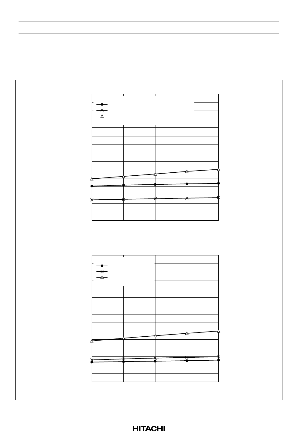
Characteristic Curves
HA12226F
(mA)
Q
Quiescent Current I
HA12226F/HA12227F
Quiescent Current vs. Supply Voltage (REC mode)
35
REC mode
NR-OFF, REC-MUTE ON, BIAS OFF
NR-OFF, REC-MUTE OFF, BIAS OFF
NR-ON, REC-MUTE OFF, BIAS ON
Other switch is all Low
30
25
20
11
Quiescent Current vs. Supply Voltage (PB mode)
35
PB mode
NR-OFF, BIAS OFF
NR-ON, BIAS OFF
NR-ON, BIAS ON
Other switch is all Low
30
(mA)
Q
25
Quiescent Current I
20
11
12 13 14
Supply Voltage (V)
12 13 14
Supply Voltage (V)
15
15
Rev.6, Dec. 2000, page 25 of 86
Page 26
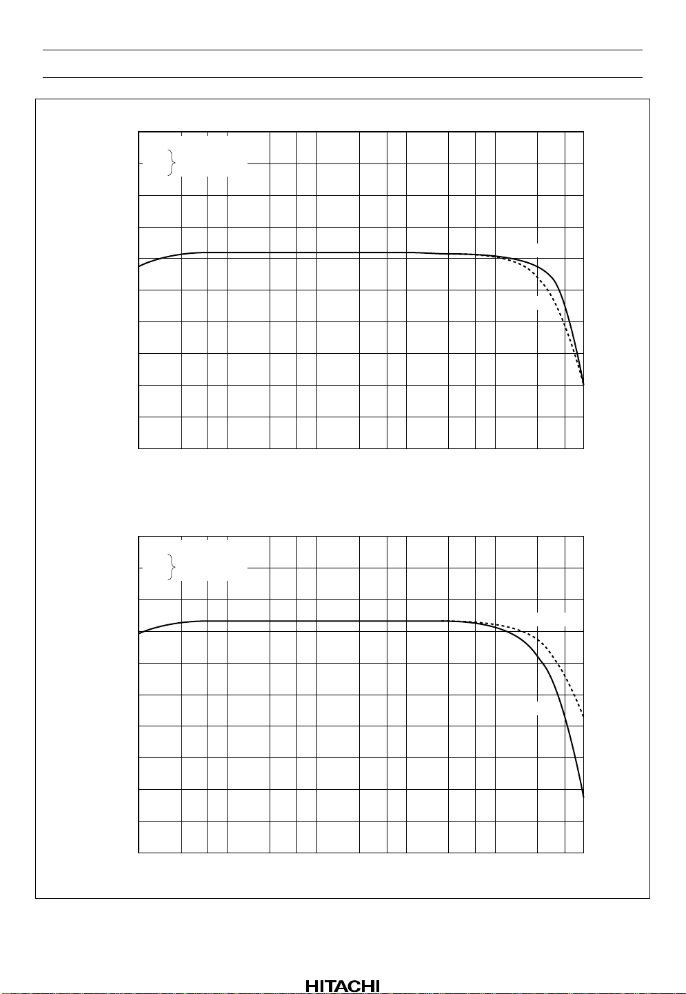
HA12226F/HA12227F
40
VCC = 12V
Ain
→ RECOUT
Bin
30
Input Amp. Gain vs. Frequency (1)
20
Gain (dB)
10
0
−10
10
40
VCC = 12V
Ain
Bin
30
100 1k 10k 100k
Frequency (Hz)
Input Amp. Gain vs. Frequency (2)
→ PBOUT
NR-ON
NR-OFF
1M
PASS mode
20
Gain (dB)
10
0
−10
10
Rev.6, Dec. 2000, page 26 of 86
100 1k 10k 100k
Frequency (Hz)
PB mode
1M
Page 27

40
HA12226F/HA12227F
Input Amp. Gain vs. Frequency (3)
VCC = 12V
REC mode
30
20
Gain (dB)
10
0
−10
10
30
VCC = 12V
Ain
Bin
26
PBOUT
RECOUT
100 1k 10k 100k
Frequency (Hz)
Input Amp. Gain vs. Frequency (4)
→ PBOUT
120µ
1M
22
Gain (dB)
18
14
10
10
70µ
100 1k 10k 100k
Frequency (Hz)
Rev.6, Dec. 2000, page 27 of 86
1M
Page 28

HA12226F/HA12227F
12
VCC = 12V
Dolby B-NR
10
8
6
Encode Boost (dB)
4
Encode Boost vs. Frequency
−40dB
−30dB
−20dB
2
0
100
0
−2
−4
−6
Decode Cut (dB)
−8
−10dB
0dB
1k 20k10k
Frequency (Hz)
Decode Cut vs. Frequency
0dB
−10dB
−20dB
−30dB
−10
VCC = 12V
Dolby B-NR
−12
100
Rev.6, Dec. 2000, page 28 of 86
−40dB
1k 20k10k
Frequency (Hz)
Page 29

Signal Handling (1)
30
REC mode
Rin → RECOUT = 300mVrms = 0dB
f = 1kHz, T.H.D. ≈ 1%
NR-OFF
NR-ON
25
Vomax (dB)
20
15
11
12 13 14
Supply Voltage (V)
HA12226F/HA12227F
15
25
Ain
→ PBOUT = 580mVrms = 0dB
Bin
f = 1kHz, T.H.D. ≈ 1%
NR-OFF
NR-ON
PASS mode
20
Vomax (dB)
15
10
11
Signal Handling (2)
PB mode
12 13 14
Supply Voltage (V)
15
Rev.6, Dec. 2000, page 29 of 86
Page 30

HA12226F/HA12227F
85
Signal to Noise Ratio vs. Split Supply Voltage (1)
A, Bin, PB mode, NR-ON
Rin, REC mode, NR-OFF
80
A, Bin, PB mode, NR-OFF
f = 1kHz, CCIR/ARM filter
75
Rin → RECOUT = 300mVrms = 0dB
Ain
→ PBOUT = 580mVrms = 0dB
Bin
Signal to Noise Ratio (dB)
Rin, PEC mode, NR-ON
70
65
11
Total Harmonic Distortion vs. Supply Voltage (1)
1.0
REC mode, NR-OFF
Rin → RECOUT = 300mVrms
Rin → PBOUT = 580mVrms
12 13 14
(REC mode, NR-OFF)
100Hz (30kHz LPF)
1kHz (400Hz HPF + 30kHz LPF)
10kHz (400Hz HPF + 80kHz LPF)
1kHz (400Hz HPF + 30kHz LPF)
Supply Voltage (V)
A, Bin, PASS mode, PBOUT
15
0.1
T.H.D. (%)
0.01
11
Rev.6, Dec. 2000, page 30 of 86
12 13 14
Supply Voltage (V)
15
Page 31

HA12226F/HA12227F
Total Harmonic Distortion vs. Supply Voltage (2)
1.0
REC mode, NR-ON
Rin → RECOUT = 300mVrms
100Hz (30kHz LPF)
1kHz (400Hz HPF + 30kHz LPF)
10kHz (400Hz HPF + 80kHz LPF)
Rin → PBOUT = 580mVrms
1kHz (400Hz HPF + 30kHz LPF)
0.1
T.H.D. (%)
0.01
11
12 13 14
(REC mode, NR-ON)
15
Supply Voltage (V)
1.0
PB mode, NR-OFF
Ain
Bin
Ain
Bin
0.1
T.H.D. (%)
0.01
11
Total Harmonic Distortion vs. Supply Voltage (3)
(PB mode, NR-OFF)
→ PBOUT = 580mVrms
100Hz (30kHz LPF)
1kHz (400Hz HPF + 30kHz LPF)
10kHz (400Hz HPF + 80kHz LPF)
→ RECOUT = 300mVrms
1kHz (400Hz HPF + 30kHz LPF)
12 13 14
Supply Voltage (V)
15
Rev.6, Dec. 2000, page 31 of 86
Page 32

HA12226F/HA12227F
1.0
PB mode, NR-ON
Ain
Bin
Ain
Bin
0.1
T.H.D. (%)
0.01
11
Total Harmonic Distortion vs. Supply Voltage (4)
(PB mode, NR-ON)
→ PBOUT = 580mVrms
100Hz (30kHz LPF)
1kHz (400Hz HPF + 30kHz LPF)
10kHz (400Hz HPF + 80kHz LPF)
→ RECOUT = 300mVrms
1kHz (400Hz HPF + 30kHz LPF)
12 13 14
Supply Voltage (V)
15
1.0
PASS mode, NR
Ain
Bin
0.1
T.H.D. (%)
0.01
11
Total Harmonic Distortion vs. Supply Voltage (5)
(PASS mode, NR-OFF)
ON
OFF
→ PBOUT = 580mVrms
100Hz (30kHz LPF)
1kHz (400Hz HPF + 30kHz LPF)
10kHz (400Hz HPF + 80kHz LPF)
12 13 14
Supply Voltage (V)
15
Rev.6, Dec. 2000, page 32 of 86
Page 33

HA12226F/HA12227F
Total Harmonic Distortion vs. Output Level (1)
10
REC mode, NR-OFF
= 12V
V
CC
100Hz
1kHz
10kHz
Rin RECOUT = 300mVrms = 0dB
1.0
T.H.D. (%)
0.1
0.01
10
5
(REC mode, NR-OFF)
Output Level Vout (dB)
15 201050
Total Harmonic Distortion vs. Output Level (2)
10
REC mode, NR-ON
= 12V
V
CC
100Hz
1kHz
10kHz
Rin RECOUT = 300mVrms = 0dB
1.0
T.H.D. (%)
0.1
0.01
10
5
(REC mode, NR-ON)
Output Level Vout (dB)
15 201050
Rev.6, Dec. 2000, page 33 of 86
Page 34

HA12226F/HA12227F
10
PB mode, NR-OFF
V
CC
Ain
Bin
1.0
T.H.D. (%)
0.1
0.01
−10
Total Harmonic Distortion vs. Output Level (3)
(PB mode, NR-OFF)
= 12V
100Hz
1kHz
10kHz
→ PBOUT = 580mVrms = 0dB
15 201050−5
Output Level Vout (dB)
10
PB mode, NR-ON
V
CC
Ain
Bin
1.0
T.H.D. (%)
0.1
0.01
−10
Total Harmonic Distortion vs. Output Level (4)
(PB mode, NR-ON)
= 12V
100Hz
1kHz
10kHz
→ PBOUT = 580mVrms = 0dB
15 201050−5
Output Level Vout (dB)
Rev.6, Dec. 2000, page 34 of 86
Page 35

HA12226F/HA12227F
Total Harmonic Distortion vs. Output Level (5)
10
PASS mode, NR-OFF
V
= 12V
CC
Ain
Bin
1.0
T.H.D. (%)
0.1
0.01
−10
(PASS mode, NR-OFF)
100Hz
1kHz
10kHz
→ PBOUT = 580mVrms = 0dB
15 201050−5
Output Level Vout (dB)
REC mode, NR-OFF, VCC = 12V
Rin → RECOUT = 300mVrms
0.1
T.H.D. (%)
0.01
Total Harmonic Distortion vs. Frequency (1)
−10dB
0dB
10dB
100 1k 10k 100k
Frequency (Hz)
Rev.6, Dec. 2000, page 35 of 86
Page 36

HA12226F/HA12227F
REC mode, NR-ON, VCC = 12V
Rin → RECOUT = 300mVrms
−10dB
0dB
10dB
0.1
T.H.D. (%)
Total Harmonic Distortion vs. Frequency (2)
0.01
PB mode, NR-OFF, VCC = 12V
Ain
Bin
0.1
T.H.D. (%)
100 1k 10k 100k
Frequency (Hz)
Total Harmonic Distortion vs. Frequency (3)
→ PBOUT = 580mVrms
−10dB
0dB
10dB
0.01
100 1k 10k 100k
Rev.6, Dec. 2000, page 36 of 86
Frequency (Hz)
Page 37

PB mode, NR-ON, VCC = 12V
Ain
Bin
0.1
T.H.D. (%)
HA12226F/HA12227F
Total Harmonic Distortion vs. Frequency (4)
→ PBOUT = 580mVrms
−10dB
0dB
10dB
0.01
PASS mode, NR-OFF, VCC = 12V
Ain
Bin
0.1
T.H.D. (%)
100 1k 10k 100k
Frequency (Hz)
Total Harmonic Distortion vs. Frequency (5)
→ PBOUT = 580mVrms
−10dB
0dB
10dB
0.01
100 1k 10k 100k
Frequency (Hz)
Rev.6, Dec. 2000, page 37 of 86
Page 38

HA12226F/HA12227F
−40
VCC = 11V, 12V, 15V
Rin → RECOUT, Vin = +12dB
REC mode, R → L
−60
−80
−100
Channel Separation (dB)
−120
Channel Separation vs. Frequency (R → L) (1)
NR-ON
NR-OFF
−140
−40
VCC = 11V, 12V, 15V
Rin → PBOUT, Vin = +12dB
REC mode, R → L
−60
−80
−100
Channel Separation (dB)
−120
10010 1k 10k 100k
Frequency (Hz)
Channel Separation vs. Frequency (R → L) (2)
NR-ON/OFF
−140
Rev.6, Dec. 2000, page 38 of 86
10010 1k 10k 100k
Frequency (Hz)
Page 39

Channel Separation vs. Frequency (L → R) (3)
−40
VCC = 11V, 12V, 15V
Rin → RECOUT, Vin = +12dB
REC mode, L → R
−60
HA12226F/HA12227F
−80
−100
Channel Separation (dB)
−120
−140
−40
VCC = 11V, 12V, 15V
Rin → PBOUT, Vin = +12dB
REC mode, L → R
−60
NR-ON
NR-OFF
10010 1k 10k 100k
Frequency (Hz)
Channel Separation vs. Frequency (L → R) (4)
−80
−100
Channel Separation (dB)
−120
−140
NR-ON/OFF
10010 1k 10k 100k
Frequency (Hz)
Rev.6, Dec. 2000, page 39 of 86
Page 40

HA12226F/HA12227F
−20
VCC = 11V, 12V, 15V
Ain → PBOUT, Vin = +10dB
R → L
−40
−60
−80
Channel Separation (dB)
−100
Channel Separation vs. Frequency (R → L) (1)
NR-OFF
NR-ON
−120
−20
VCC = 11V, 12V, 15V
Ain → RECOUT, Vin = +10dB
R → L
−40
−60
−80
Channel Separation (dB)
−100
10010 1k 10k 100k
Frequency (Hz)
Channel Separation vs. Frequency (R → L) (2)
NR-ON/OFF
−120
Rev.6, Dec. 2000, page 40 of 86
10010 1k 10k 100k
Frequency (Hz)
Page 41

−20
VCC = 11V, 12V, 15V
Bin → PBOUT, Vin = +10dB
R → L
−40
−60
−80
Channel Separation (dB)
−100
HA12226F/HA12227F
Channel Separation vs. Frequency (R → L) (3)
NR-OFF
NR-ON
−120
−20
VCC = 11V, 12V, 15V
Bin → RECOUT, Vin = +10dB
R → L
−40
−60
−80
Channel Separation (dB)
−100
10010 1k 10k 100k
Frequency (Hz)
Channel Separation vs. Frequency (R → L) (4)
NR-ON/OFF
−120
10010 1k 10k 100k
Frequency (Hz)
Rev.6, Dec. 2000, page 41 of 86
Page 42

HA12226F/HA12227F
−20
VCC = 11V, 12V, 15V
Ain → PBOUT, Vin = +10dB
L → R
−40
−60
−80
Channel Separation (dB)
−100
Channel Separation vs. Frequency (L → R) (5)
NR-OFF
NR-ON
−120
−20
VCC = 11V, 12V, 15V
Ain → RECOUT, Vin = +10dB
L → R
−40
−60
−80
Channel Separation (dB)
−100
10010 1k 10k 100k
Frequency (Hz)
Channel Separation vs. Frequency (L → R) (6)
NR-ON/OFF
−120
Rev.6, Dec. 2000, page 42 of 86
10010 1k 10k 100k
Frequency (Hz)
Page 43

−20
VCC = 11V, 12V, 15V
Bin → PBOUT, Vin = +10dB
L → R
−40
−60
−80
Channel Separation (dB)
−100
HA12226F/HA12227F
Channel Separation vs. Frequency (L → R) (7)
NR-OFF
NR-ON
−120
−20
VCC = 11V, 12V, 15V
Bin → RECOUT, Vin = +10dB
L → R
−40
−60
−80
Channel Separation (dB)
−100
10010 1k 10k 100k
Frequency (Hz)
Channel Separation vs. Frequency (L → R) (8)
NR-ON/OFF
−120
10010 1k 10k 100k
Frequency (Hz)
Rev.6, Dec. 2000, page 43 of 86
Page 44

HA12226F/HA12227F
−20
VCC = 11V, 12V, 15V
Ain
→ PBOUT, Vin = +10dB
Bin
PASS mode, R → L
−40
−60
Channel Separation vs. Frequency (R → L) (1)
Ain
−80
Channel Separation (dB)
−100
−120
−20
VCC = 11V, 12V, 15V
Ain
→ PBOUT, Vin = +10dB
Bin
PASS mode, L → R
−40
−60
Bin
10010 1k 10k 100k
Frequency (Hz)
Channel Separation vs. Frequency (L → R) (2)
Ain
−80
Channel Separation (dB)
−100
−120
Rev.6, Dec. 2000, page 44 of 86
Bin
10010 1k 10k 100k
Frequency (Hz)
Page 45

−40
VCC = 11V, 12V, 15V
PB mode, PBOUT
Vin = +12dB, Ain → Bin
HA12226F/HA12227F
Crosstalk vs. Frequency (Ain → Bin) (1)
−60
−80
−100
Crosstalk (dB)
−120
−140
−40
VCC = 11V, 12V, 15V
PB mode, PBOUT
Vin = +12dB, Bin → Ain
NR-OFF
NR-ON
10010 1k 10k 100k
Frequency (Hz)
Crosstalk vs. Frequency (Bin → Ain) (2)
−60
−80
−100
Crosstalk (dB)
−120
−140
NR-OFF
NR-ON
10010 1k 10k 100k
Frequency (Hz)
Rev.6, Dec. 2000, page 45 of 86
Page 46

HA12226F/HA12227F
Crosstalk vs. Frequency (PB mode → PASS mode) (1)
−20
VCC = 11V, 12V, 15V
Ain → RECOUT
Vin = +12dB
PB mode → PASS mode
−40
−60
−80
Crosstalk (dB)
−100
−120
−20
VCC = 11V, 12V, 15V
Bin → RECOUT
Vin = +12dB
PB mode → PASS mode
−40
−60
−80
Crosstalk (dB)
−100
10010 1k 10k 100k
Frequency (Hz)
Crosstalk vs. Frequency (PB mode → PASS mode) (2)
−120
Rev.6, Dec. 2000, page 46 of 86
10010 1k 10k 100k
Frequency (Hz)
Page 47

−20
VCC = 12V
Ain
→ PBOUT
Bin
Vin = +12dB
−40
PB mode
−60
−80
Line Mute (dB)
−100
HA12226F/HA12227F
Line Mute vs. Frequency
−120
80
VCC = 12V
EQIN → EQOUT
Vin = +14dB
Norm speed, Norm tape
40
0
−40
Crosstalk (dB)
−80
10010 1k 10k 100k
Frequency (Hz)
REC Mute Attenuation vs. Frequency
−120
10010 1k 10k 100k
Frequency (Hz)
Rev.6, Dec. 2000, page 47 of 86
Page 48

HA12226F/HA12227F
Ripple Rejection Ratio vs. Frequency (REC mode) (1)
20
VCC = 12V
REC mode
0
−20
EQOUT
RECOUT
NR-ON
−40
Ripple Rejection Ratio R.R.R. (dB)
−60
−80
20
VCC = 12V
PB mode
0
−20
10010 1k 10k 100k
Ripple Rejection Ratio vs. Frequency (PB mode) (2)
Frequency (Hz)
PBOUT
NR-OFF
PBOUT
RECOUT
NR-OFF
EQOUT
−40
Ripple Rejection Ratio R.R.R. (dB)
−60
−80
Rev.6, Dec. 2000, page 48 of 86
RECOUT
10010 1k 10k 100k
Frequency (Hz)
PBOUT
NR-ON
Page 49

20
VCC = 12V
PASS mode
0
HA12226F/HA12227F
Ripple Rejection Ratio vs. Frequency (PASS mode) (3)
EQOUT
−20
−40
Ripple Rejection Ratio R.R.R. (dB)
−60
−80
55
50
45
40
VCC = 12V
Norm speed
10010 1k 10k 100k
Equalizer Amp. Gain vs. Frequency (1)
RECOUT
NR-ON
Frequency (Hz)
PBOUT
RECOUT
NR-OFF
35
30
25
REC-EQ Gain (dB)
20
15
10
5
Crom
Norm
10010 1k 10k 100k
Frequency (Hz)
Rev.6, Dec. 2000, page 49 of 86
Page 50

HA12226F/HA12227F
55
VCC = 12V
High speed
50
45
40
35
30
25
REC-EQ Gain (dB)
20
Equalizer Amp. Gain vs. Frequency (2)
Crom
15
10
5
55
50
45
40
35
30
25
REC-EQ Gain (dB)
20
15
10
Norm
10010 1k 10k 100k
Frequency (Hz)
Equalizer Amp. Gain vs. Frequency (REC-cal)
REC-cal = 5V
REC-cal = 2.5V
REC-cal = 0V
5
Rev.6, Dec. 2000, page 50 of 86
10010 1k 10k 100k
Frequency (Hz)
Page 51

55
50
45
40
35
HA12226F/HA12227F
Equalizer Amp. Gain vs. Frequency (GP-cal)
GP-cal = 0V
30
25
REC-EQ Gain (dB)
20
15
10
5
70
65
GP-cal = 2.5V
GP-cal = 5V
10010 1k 10k 100k
Frequency (Hz)
Equalizer Signal to Noise Ratio vs. Supply Voltage (1)
f = 1kHz
A-WTG filter
Norm speed
NN
NC
REC-EQ S/N (dB)
60
55
11
12 13 14
Supply Voltage (V)
15
Rev.6, Dec. 2000, page 51 of 86
Page 52

HA12226F/HA12227F
Equalizer Signal to Noise Ratio vs. Supply Voltage (2)
70
f = 1kHz
A-WTG filter
High speed
65
REC-EQ S/N (dB)
60
55
11
HN
HC
12 13 14
Supply Voltage (V)
15
REC-cal Correction vs. V
5
f = 3kHz
GP-cal open
4
V
= 12V
CC
Norm speed
3
Norm tape
2
1
0
−1
−2
REC-cal Correction (dB)
−3
−4
−5
0
1432
V
REC-cal
REC-cal
5
(V)
Rev.6, Dec. 2000, page 52 of 86
Page 53

HA12226F/HA12227F
GP-cal Correction vs. V
5
4
3
2
1
0
−1
GP-cal Correction (dB)
−2
f = 12kHz
−3
REC-cal open
V
= 12V
CC
−4
Norm speed
Norm tape
−5
0
1432
V
GP-cal
GP-cal
5
(V)
10
f = 1kHz, VCC = 12V, Both channel input (L, Rch)
Rin → RECOUT,
8
6
4
2
0
Output Level RECOUT (dB) 0dB ≈ 300mVrms
−2
−53020100
Norm
Crom
ALC Operate Level vs. Input Level
Cal = 5V
Cal = 5V
Cal = 2.5V
Cal = 2.5V
Cal = 0V
Cal = 0V
51525
Input Level Vin (dB) 0dB ≈ 221mVrms
35
Rev.6, Dec. 2000, page 53 of 86
Page 54

HA12226F/HA12227F
ALC Total Harmonic Distortion vs. Input Level (1)
f = 1kHz, V
Norm tape
Cal = 0V
Cal = 2.5V
1.0
ALC T.H.D. (%)
0.1
0.01
−5
Cal = 5V
Input Level Vin (dB) 0dB ≈ 221mVrms
ALC Total Harmonic Distortion vs. Input Level (2)
CC
= 12V
20 25151050
(ALC-OFF, RECOUT ≈ 300mVrms)
30
f = 1kHz, V
Crom tape
Cal = 0V
Cal = 2.5V
1.0
ALC T.H.D. (%)
0.1
0.01
−5
Cal = 5V
Input Level Vin (dB) 0dB ≈ 221mVrms
CC
= 12V
20 25151050
(ALC-OFF, RECOUT ≈ 300mVrms)
30
Rev.6, Dec. 2000, page 54 of 86
Page 55

10
HA12226F/HA12227F
ALC Operate Level vs. Frequency
8
6
4
2
0
−2
Operate Level RECOUT (dB) 0dB = 300mVrms
−4
Vin = +12dB, Both channel input (L, Rch), Rin → RECOUT
Norm
Crom
100 1k 10k
Frequency (Hz)
Bias Output Voltage vs. Load Current
13
VCC = 12V
Bias ON
270Ω
31
V
ALC-cal = 5V
ALC-cal = 5V
ALC-cal = 2.5V
ALC-cal = 2.5V
ALC-cal = 0V
ALC-cal = 0V
I
12
11
Bias Output Voltage (V)
10
0
Load Current I (mA)
564321
Rev.6, Dec. 2000, page 55 of 86
7
Page 56

HA12226F/HA12227F
5
0
−5
−10
−15
MS Sensing Level (dB)
−20
−25
−30
100 1k 10k 100k
MS Sensing Level vs. Frequency
VCC = 12V, MSOUT
Ain → PBOUT = 580mVrms = 0dB
Lo → Hi
Hi → Lo
Frequency (Hz)
40
30
20
Gain (dB)
10
0
−10
MS Amp. Gain vs. Frequency
VCC = 12V
MAOUT
MSIN
10010 1k 10k 100k
Frequency (Hz)
Rev.6, Dec. 2000, page 56 of 86
Page 57

No-Signal Sensing Time vs. Resistance
1000
VCC = 12V, f = 5kHz
Ain → PBOUT = 580mVrms
0dB
−10dB
−20dB
100
10
No-Signal Sensing Time (ms)
HA12226F/HA12227F
PBOUT
MSOUT
C13
0.33µ
14 V
R13
1
10k 100k 1M
Resistance R13 (Ω)
Signal Sensing Time vs. Capacitance
VCC = 12V, f = 5kHz
Ain → PBOUT = 580mVrms
0dB
100
−10dB
−20dB
10
PBOUT
1
Signal Sensing Time (ms)
0.1
MSOUT
14 V
C13
R13
330k
0.01 0.1 1.0
Capacitance C13 (µF)
CC
CC
Rev.6, Dec. 2000, page 57 of 86
Page 58

HA12226F/HA12227F
HA12227F
30
REC mode
Other switch is all Low
25
(mA)
Q
20
Quiescent Current I
Quiescent Current vs. Supply Voltage (REC mode)
REC-MUTE ON, BIAS OFF
REC-MUTE OFF, BIAS OFF
REC-MUTE OFF, BIAS ON
15
11
Quiescent Current vs. Supply Voltage (PB mode)
30
PB mode
REC-MUTE ON, BIAS OFF
REC-MUTE OFF, BIAS OFF
REC-MUTE OFF, BIAS ON
Other switch is all Low
25
(mA)
Q
20
Quiescent Current I
15
11
12 13 14
Supply Voltage (V)
12 13 14
Supply Voltage (V)
15
15
Rev.6, Dec. 2000, page 58 of 86
Page 59

50
VCC = 12V
Ain
Bin
PB mode
40
30
Gain (dB)
20
10
HA12226F/HA12227F
Input Amp. Gain vs. Frequency (1)
→ PBOUT
0
10
50
VCC = 12V
Ain
Bin
PASS mode
40
30
Gain (dB)
20
10
100 1k 10k 100k
Frequency (Hz)
Input Amp. Gain vs. Frequency (2)
→ PBOUT
1M
0
10
100 1k 10k 100k
Frequency (Hz)
Rev.6, Dec. 2000, page 59 of 86
1M
Page 60

HA12226F/HA12227F
50
VCC = 12V
REC mode
40
Input Amp. Gain vs. Frequency (3)
30
Gain (dB)
20
10
0
10
50
VCC = 12V
Ain
Bin
40
PBOUT
RECOUT
100 1k 10k 100k
Frequency (Hz)
Input Amp. Gain vs. Frequency (4)
→ PBOUT
1M
30
Gain (dB)
20
10
0
10
Rev.6, Dec. 2000, page 60 of 86
120µ
70µ
100 1k 10k 100k
Frequency (Hz)
1M
Page 61

Signal Handling (1)
25
20
Vomax (dB)
15
REC mode, T.H.D. ≈ 1%
Rin → RECOUT = 300mVrms = 0dB
1kHz
Rin → PBOUT = 580mVrms = 0dB
10
11
1kHz
12 13 14
Supply Voltage (V)
HA12226F/HA12227F
15
25
20
Vomax (dB)
15
PB mode, T.H.D. ≈ 1%
Ain
→ RECOUT = 300mVrms = 0dB
Bin
1kHz
Ain
→ PBOUT = 580mVrms = 0dB
Bin
10
11
1kHz
Signal Handling (2)
12 13 14
Supply Voltage (V)
15
Rev.6, Dec. 2000, page 61 of 86
Page 62

HA12226F/HA12227F
85
80
75
Signal to Noise Ratio (dB)
REC mode, CCIR/ARM filter
Rin → RECOUT = 300mVrms = 0dB
Rin → PBOUT = 580mVrms = 0dB
70
11
Signal to Noise Ratio vs. Supply Voltage (1)
1kHz
1kHz
12 13 14
Supply Voltage (V)
15
Signal to Noise Ratio vs. Supply Voltage (2)
85
80
75
PB mode, CCIR/ARM filter
Signal to Noise Ratio (dB)
Ain
→ RECOUT = 300mVrms = 0dB
Bin
1kHz
Ain
→ PBOUT = 580mVrms = 0dB
Bin
70
11
1kHz
12 13 14
Supply Voltage (V)
15
Rev.6, Dec. 2000, page 62 of 86
Page 63

Signal to Noise Ratio vs. Supply Voltage (3)
85
PASS mode, CCIR/ARM filter
Ain
→ PBOUT = 580mVrms = 0dB
Bin
1kHz
80
75
Signal to Noise Ratio (dB)
70
11
12 13 14
Supply Voltage (V)
HA12226F/HA12227F
15
Total Harmonic Distortion vs. Supply Voltage (1)
1.0
REC mode
Rin → RECOUT = 300mVrms
100Hz (30kHz LPF)
1kHz (400Hz HPF + 30kHz LPF)
10kHz (400Hz HPF + 80kHz LPF)
Rin → PBOUT = 580mVrms
1kHz (400Hz HPF + 30kHz LPF)
0.1
T.H.D. (%)
0.01
11
12 13 14
15
Supply Voltage (V)
Rev.6, Dec. 2000, page 63 of 86
Page 64

HA12226F/HA12227F
1.0
PB mode, NR-OFF
Ain
Bin
Ain
Bin
0.1
T.H.D. (%)
0.01
11
Total Harmonic Distortion vs. Supply Voltage (2)
→ PBOUT = 580mVrms
100Hz (30kHz LPF)
1kHz (400Hz HPF + 30kHz LPF)
10kHz (400Hz HPF + 80kHz LPF)
→ RECOUT = 300mVrms
1kHz (400Hz HPF + 30kHz LPF)
12 13 14
Supply Voltage (V)
15
Total Harmonic Distortion vs. Supply Voltage (3)
1.0
PASS mode
Ain → PBOUT = 580mVrms
100Hz (30kHz LPF)
1kHz (400Hz HPF + 30kHz LPF)
10kHz (400Hz HPF + 80kHz LPF)
0.1
T.H.D. (%)
0.01
11
12 13 14
15
Supply Voltage (V)
Rev.6, Dec. 2000, page 64 of 86
Page 65

10
REC mode
Rin → RECOUT
0dB = 300mVrms
V
CC
1.0
T.H.D. (%)
0.1
0.01
−15
HA12226F/HA12227F
Total Harmonic Distortion vs. Output Level (1)
= 12V
100Hz
1kHz
10kHz
15 25201050−10 −5
Output Level Vout (dB)
10
PB mode
Ain
Bin
0dB = 580mVrms
V
CC
1.0
T.H.D. (%)
0.1
0.01
−15
Total Harmonic Distortion vs. Output Level (2)
→ PBOUT
= 12V
100Hz
1kHz
10kHz
15 25201050−10 −5
Output Level Vout (dB)
Rev.6, Dec. 2000, page 65 of 86
Page 66

HA12226F/HA12227F
10
PASS mode
Ain
Bin
0dB = 580mVrms
V
1.0
T.H.D. (%)
0.1
0.01
−15
Total Harmonic Distortion vs. Output Level (3)
→ PBOUT
= 12V
CC
100Hz
1kHz
10kHz
15 25201050−10 −5
Output Level Vout (dB)
REC mode
Rin → RECOUT
0dB = 300mVrms
0.1
T.H.D. (%)
0.01
Total Harmonic Distortion vs. Frequency (1)
−10dB
0dB
10dB
100 1k 10k 100k
Frequency (Hz)
Rev.6, Dec. 2000, page 66 of 86
Page 67

PB mode
Ain
Bin
0dB = 580mVrms
0.1
T.H.D. (%)
HA12226F/HA12227F
Total Harmonic Distortion vs. Frequency (2)
→ PBOUT
−10dB
0dB
10dB
0.01
PB mode
Ain
Bin
0dB = 580mVrms
0.1
T.H.D. (%)
100 1k 10k 100k
Frequency (Hz)
Total Harmonic Distortion vs. Frequency (3)
→ PBOUT
−10dB
0dB
10dB
0.01
100 1k 10k 100k
Frequency (Hz)
Rev.6, Dec. 2000, page 67 of 86
Page 68

HA12226F/HA12227F
40
VCC = 11V, 12V, 15V
Rin → RECOUT, Vin = +12dB
REC mode, R → L
0
−40
−80
Channel Separation (dB)
−120
Channel Separation vs. Frequency (R → L) (1)
−160
40
VCC = 11V, 12V, 15V
Rin → RECOUT, Vin = +12dB
REC mode, L → R
0
−40
−80
Channel Separation (dB)
−120
10010 1k 10k 100k
Frequency (Hz)
Channel Separation vs. Frequency (L → R) (2)
−160
Rev.6, Dec. 2000, page 68 of 86
10010 1k 10k 100k
Frequency (Hz)
Page 69

40
VCC = 11V, 12V, 15V
Ain → PBOUT, Vin = +10dB
R → L
0
−40
−80
Channel Separation (dB)
−120
HA12226F/HA12227F
Channel Separation vs. Frequency (R → L) (3)
−160
40
VCC = 11V, 12V, 15V
Ain → PBOUT, Vin = +10dB
L → R
0
−40
−80
Channel Separation (dB)
−120
10010 1k 10k 100k
Frequency (Hz)
Channel Separation vs. Frequency (L → R) (4)
−160
10010 1k 10k 100k
Frequency (Hz)
Rev.6, Dec. 2000, page 69 of 86
Page 70

HA12226F/HA12227F
40
VCC = 11V, 12V, 15V
Bin → PBOUT, Vin = +10dB
R → L
0
−40
−80
Channel Separation (dB)
−120
Channel Separation vs. Frequency (R → L) (5)
−160
40
VCC = 11V, 12V, 15V
Bin → PBOUT, Vin = +10dB
L → R
0
−40
−80
Channel Separation (dB)
−120
10010 1k 10k 100k
Frequency (Hz)
Channel Separation vs. Frequency (L → R) (6)
−160
Rev.6, Dec. 2000, page 70 of 86
10010 1k 10k 100k
Frequency (Hz)
Page 71

40
VCC = 11V, 12V, 15V
Ain → PBOUT, Vin = +10dB
PASS mode, R → L
0
−40
−80
Channel Separation (dB)
−120
HA12226F/HA12227F
Channel Separation vs. Frequency (R → L) (7)
−160
40
VCC = 11V, 12V, 15V
Ain → PBOUT, Vin = +10dB
PASS mode, L → R
0
−40
−80
Channel Separation (dB)
−120
10010 1k 10k 100k
Frequency (Hz)
Channel Separation vs. Frequency (L → R) (8)
−160
10010 1k 10k 100k
Frequency (Hz)
Rev.6, Dec. 2000, page 71 of 86
Page 72

HA12226F/HA12227F
40
VCC = 11V, 12V, 15V
Bin → PBOUT, Vin = +10dB
PASS mode, R → L
0
−40
−80
Channel Separation (dB)
−120
Channel Separation vs. Frequency (R → L) (9)
−160
Channel Separation vs. Frequency (L → R) (10)
40
VCC = 11V, 12V, 15V
Bin → PBOUT, Vin = +10dB
PASS mode, L → R
0
−40
−80
Channel Separation (dB)
−120
10010 1k 10k 100k
Frequency (Hz)
−160
Rev.6, Dec. 2000, page 72 of 86
10010 1k 10k 100k
Frequency (Hz)
Page 73

40
VCC = 11V, 12V, 15V
PB mode, PBOUT
Vin = +12dB, Ain → Bin
0
−40
−80
Channel Separation (dB)
−120
HA12226F/HA12227F
Crosstalk vs. Frequency (Ain → Bin) (1)
−160
40
VCC = 11V, 12V, 15V
PB mode, PBOUT
Vin = +12dB, Bin → Ain
0
−40
−80
Channel Separation (dB)
−120
10010 1k 10k 100k
Frequency (Hz)
Crosstalk vs. Frequency (Bin → Ain) (2)
−160
10010 1k 10k 100k
Frequency (Hz)
Rev.6, Dec. 2000, page 73 of 86
Page 74

HA12226F/HA12227F
40
VCC = 12V
Ain
→ PBOUT
Bin
Vin = +12dB
0
PB mode
−40
−80
Line Mute (dB)
−120
Line Mute vs. Frequency
−160
40
VCC = 12V
EQIN → EQOUT
Vin = +14dB
Norm speed, Norm tape
0
−40
−80
Crosstalk (dB)
−120
10010 1k 10k 100k
Frequency (Hz)
REC Mute Attenuation vs. Frequency
−160
Rev.6, Dec. 2000, page 74 of 86
10010 1k 10k 100k
Frequency (Hz)
Page 75

20
0
−20
HA12226F/HA12227F
Ripple Rejection Ratio vs. Frequency (REC mode) (1)
VCC = 12V
REC mode
EQOUT
−40
Ripple Rejection Ratio R.R.R. (dB)
−60
−80
20
VCC = 12V
PB mode, RECOUT
0
−20
10010 1k 10k 100k
Ripple Rejection Ratio vs. Frequency (PB mode) (2)
RECOUT
Frequency (Hz)
−40
Ripple Rejection Ratio R.R.R. (dB)
−60
−80
10010 1k 10k 100k
Frequency (Hz)
Rev.6, Dec. 2000, page 75 of 86
Page 76

HA12226F/HA12227F
Ripple Rejection Ratio vs. Frequency (PASS mode) (3)
20
VCC = 12V
PASS mode, PBOUT
0
−20
−40
Ripple Rejection Ratio R.R.R. (dB)
−60
−80
55
VCC = 12V
Norm speed
50
45
40
35
30
25
REC-EQ Gain (dB)
20
15
10
10010 1k 10k 100k
Frequency (Hz)
Equalizer Amp. Gain vs. Frequency (1)
Crom
Norm
5
Rev.6, Dec. 2000, page 76 of 86
10010 1k 10k 100k
Frequency (Hz)
Page 77

55
VCC = 12V
High speed
50
45
40
35
30
25
REC-EQ Gain (dB)
20
HA12226F/HA12227F
Equalizer Amp. Gain vs. Frequency (2)
Crom
15
10
5
55
50
45
40
35
30
25
REC-EQ Gain (dB)
20
15
Norm
10010 1k 10k 100k
Frequency (Hz)
Equalizer Amp. Gain vs. Frequency (REC-cal)
REC-cal = 5V
REC-cal = 2.5V
10
REC-cal = 0V
5
10010 1k 10k 100k
Frequency (Hz)
Rev.6, Dec. 2000, page 77 of 86
Page 78

HA12226F/HA12227F
55
50
45
40
35
30
25
REC-EQ Gain (dB)
20
15
10
Equalizer Amp. Gain vs. Frequency (GP-cal)
GP-cal = 0V
GP-cal = 2.5V
GP-cal = 5V
5
70
65
REC-EQ S/N (dB)
60
10010 1k 10k 100k
Frequency (Hz)
Equalizer Signal to Noise Ratio vs. Supply Voltage (1)
f = 1kHz
A-WTG filter
Norm speed
NN
NC
55
11
Rev.6, Dec. 2000, page 78 of 86
12 13 14
Supply Voltage (V)
15
Page 79

Equalizer Signal to Noise Ratio vs. Supply Voltage (2)
70
f = 1kHz
A-WTG filter
High speed
HN
HC
65
REC-EQ S/N (dB)
60
55
11
12 13 14
Supply Voltage (V)
HA12226F/HA12227F
15
REC-cal Correction vs. V
5
f = 3kHz
GP-cal open
4
V
= 12V
CC
Norm speed
3
Norm tape
2
1
0
−1
−2
REC-cal Correction (dB)
−3
−4
−5
0
1432
V
REC-cal
REC-cal
5
(V)
Rev.6, Dec. 2000, page 79 of 86
Page 80

HA12226F/HA12227F
GP-cal Correction vs. V
5
4
3
2
1
0
−1
GP-cal Correction (dB)
−2
f = 12kHz
−3
REC-cal open
V
= 12V
CC
−4
Norm speed
Norm tape
−5
0
1432
V
GP-cal
GP-cal
5
(V)
ALC Operate Level vs. Input Level
10
f = 1kHz, VCC = 12V, Both channel input (L, Rch)
Rin → RECOUT,
Norm
8
Crom
Cal = 5V
Cal = 5V
6
Cal = 2.5V
4
Cal = 2.5V
2
Cal = 0V
0
Output Level RECOUT (dB) 0dB = 300mVrms
Cal = 0V
−2
−53020100
51525
Input Level Vin (dB) 0dB = 218mVrms
35
Rev.6, Dec. 2000, page 80 of 86
Page 81

HA12226F/HA12227F
ALC Total Harmonic Distortion vs. Input Level (1)
f = 1kHz, V
Norm tape
Cal = 0V
Cal = 2.5V
1.0
ALC T.H.D. (%)
0.1
0.01
−5
Cal = 5V
Input Level Vin (dB) 0dB ≈ 217mVrms
ALC Total Harmonic Distortion vs. Input Level (2)
CC
= 12V
20 25151050
(ALC-OFF, RECOUT = 300mVrms)
30
f = 1kHz, V
Crom tape
Cal = 0V
Cal = 2.5V
1.0
ALC T.H.D. (%)
0.1
0.01
−5
Cal = 5V
Input Level Vin (dB) 0dB ≈ 217mVrms
CC
= 12V
20 25151050
(ALC-OFF, RECOUT = 300mVrms)
30
Rev.6, Dec. 2000, page 81 of 86
Page 82

HA12226F/HA12227F
10
ALC Operate Level vs. Frequency
8
6
4
2
0
−2
Operate Level RECOUT (dB) 0dB = 300mVrms
−4
Vin = +12dB, Both channel input (L, Rch), Rin → RECOUT
Norm
Crom
100 1k 10k
Frequency (Hz)
Bias Output Voltage vs. Load Current
13
VCC = 12V
Bias ON
270Ω
31
V
ALC-cal = 5V
ALC-cal = 5V
ALC-cal = 2.5V
ALC-cal = 2.5V
ALC-cal = 0V
ALC-cal = 0V
I
12
11
Bias Output Voltage (V)
10
0
Rev.6, Dec. 2000, page 82 of 86
Load Current I (mA)
564321
7
Page 83

HA12226F/HA12227F
MS Sensing Level vs. Frequency
5
0
−5
−10
−15
MS Sensing Level (dB)
−20
−25
−30
100 1k 10k 100k
Frequency (Hz)
VCC = 12V, MSOUT
Ain → PBOUT = 580mVrms = 0dB
Lo → Hi
Hi → Lo
40
30
20
Gain (dB)
10
0
−10
MS Amp. Gain vs. Frequency
VCC = 12V
MAOUT
MSIN
10010 1k 10k 100k
Frequency (Hz)
Rev.6, Dec. 2000, page 83 of 86
Page 84

HA12226F/HA12227F
1000
VCC = 12V, f = 5kHz
Ain → PBOUT = 580mVrms
0dB
−10dB
−20dB
100
10
No-Signal Sensing Time (ms)
No-Signal Sensing Time vs. Resistance
PBOUT
MSOUT
C13
0.33µ
14 V
R13
1
10k 100k 1M
Resistance R13 (Ω)
Signal Sensing Time vs. Capacitance
VCC = 12V, f = 5kHz
Ain → PBOUT = 580mVrms
0dB
100
−10dB
−20dB
10
PBOUT
1
Signal Sensing Time (ms)
0.1
MSOUT
14 V
C13
R13
330k
0.01 0.1 1.0
Capacitance C13 (µF)
CC
CC
Rev.6, Dec. 2000, page 84 of 86
Page 85

Package Dimensions
HA12226F/HA12227F
12.8 ± 0.3
10.0
42 29
43
12.8 ± 0.3
56
1
*0.30 ± 0.08
0.27 ± 0.06
0.13
M
0.775 0.775
0.10
*Dimension including the plating thickness
Base material dimension
14
28
15
+0.1
2.20
–0.09
0.1
0.65
2.54 Max
0.15 ± 0.04
*0.17 ± 0.05
Hitachi Code
JEDEC
EIAJ
Mass
1.40
0.60 ± 0.15
(reference value)
Unit: mm
0˚ – 8˚
FP-56A
—
—
0.5 g
Rev.6, Dec. 2000, page 85 of 86
Page 86

HA12226F/HA12227F
Disclaimer
1. Hitachi neither warrants nor grants licenses of any rights of Hitachi’s or any third party’s patent,
copyright, trademark, or other intellectual property rights for information contained in this document.
Hitachi bears no responsibility for problems that may arise with third party’s rights, includ ing
intellectual property rights, in connection with u se of the information contained in this document.
2. Products and product specifications may be subject to change without notice. Confirm that you have
received the latest product standards or specifications before final design, purchase or use.
3. Hitachi makes every attempt to ensure that its products are of high quality and reliability. However,
contact Hitachi’s sales office before using the product in an application that demands especially high
quality and reliability or where its failure or malfunction may directly threaten human life or cause risk
of bodily injury, such as aerospace, aeronautics, nuclear power, combustion control, transportation,
traffic, safety equipment or medical equipment for life support.
4. Design your application so that the product is used within the ranges guaranteed by Hitachi particularly
for maximum rating, operating supply voltage range, heat radiation characteristics, installation
conditions and other characteristics. Hitachi bears no responsibility for failure or damage when used
beyond the guaranteed ranges. Even within the guaranteed ranges, consider normally foreseeable
failure rates or failure modes in semiconductor devices and employ systemic measures such as failsafes, so that the equipment incorporating Hitachi product does not cause bodily injury, fire or other
consequential damage due to operation of the Hitachi product.
5. This product is not designed to be radiation resistant.
6. No one is permitted to reproduce or duplicate, in any form, the whole or part of this document without
written approval from Hitachi.
7. Contact Hitachi’s sales office for any questions regarding this document or Hitachi semiconductor
products.
Sales Offices
Hitachi, Ltd.
Semiconductor & Integrated Circuits.
Nippon Bldg., 2-6-2, Ohte-machi, Chiyoda-ku, Tokyo 100-0004, Japan
Tel: Tokyo (03) 3270-2111 Fax: (03) 3270-5109
URL NorthAmerica : http://semiconductor.hitachi.com/
For further information write to:
Hitachi Semiconductor
(America) Inc.
179 East Tasman Drive,
San Jose,CA 95134
Tel: <1> (408) 433-1990
Fax: <1>(408) 433-0223
Europe : http://www.hitachi-eu.com/hel/ecg
Asia : http://sicapac.hitachi-asia.com
Japan : http://www.hitachi.co.jp/Sicd/indx.htm
Hitachi Europe GmbH
Electronic Components Group
Dornacher Straße 3
D-85622 Feldkirchen, Munich
Germany
Tel: <49> (89) 9 9180-0
Fax: <49> (89) 9 29 30 00
Hitachi Europe Ltd.
Electronic Components Group.
Whitebrook Park
Lower Cookham Road
Maidenhead
Berkshire SL6 8YA, United Kingdom
Tel: <44> (1628) 585000
Fax: <44> (1628) 585160
Hitachi Asia Ltd.
Hitachi Tower
16 Collyer Quay #20-00,
Singapore 049318
Tel : <65>-538-6533/538-8577
Fax : <65>-538-6933/538-3877
URL : http://www.hitachi.com.sg
Hitachi Asia Ltd.
(Taipei Branch Office)
4/F, No. 167, Tun Hwa North Road,
Hung-Kuo Building,
Taipei (105), Taiwan
Tel : <886>-(2)-2718-3666
Fax : <886>-(2)-2718-8180
Telex : 23222 HAS-TP
URL : http://www.hitachi.com.tw
Hitachi Asia (Hong Kong) Ltd.
Group III (Electronic Components)
7/F., North Tower,
World Finance Centre,
Harbour City, Canton Road
Tsim Sha Tsui, Kowloon,
Hong Kong
Tel : <852>-(2)-735-9218
Fax : <852>-(2)-730-0281
URL : http://www.hitachi.com.hk
Copyright Hitachi, Ltd., 2000. All rights reserved. Printed in Japan.
Colophon 2.0
Rev.6, Dec. 2000, page 86 of 86
 Loading...