

Page 1

HA12219NT
Audio Signal Processor for Cassette Deck
ADE-207-258A
2nd Edition
July 1998
Description
HA12219NT is silicon monolithic bipolar IC providing PB equalizer, REC equalizer system and each
electronic control switch in one chip.
Functions
• PB equalizer × 2 channel
• REC equalizer × 2 channel
• Each electronic control switch to change REC/PB etc.
• REC MUTE
• REC head return switch
Features
• REC equalizer is very small number of extern al parts, built-in 2 types of frequency characteristics.
• PB equalizer circuit built-in.
• REC /PB are possible with TYPE I/II.
• Controllable from direct micro-computer output.
• Available to reduce substrate-area because of high integration and small external parts.
Page 2
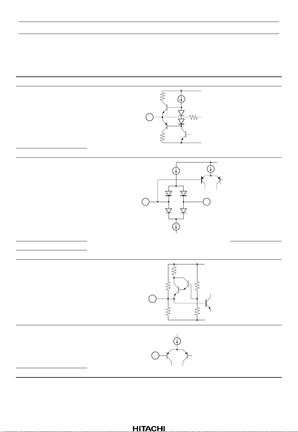
HA12219NT
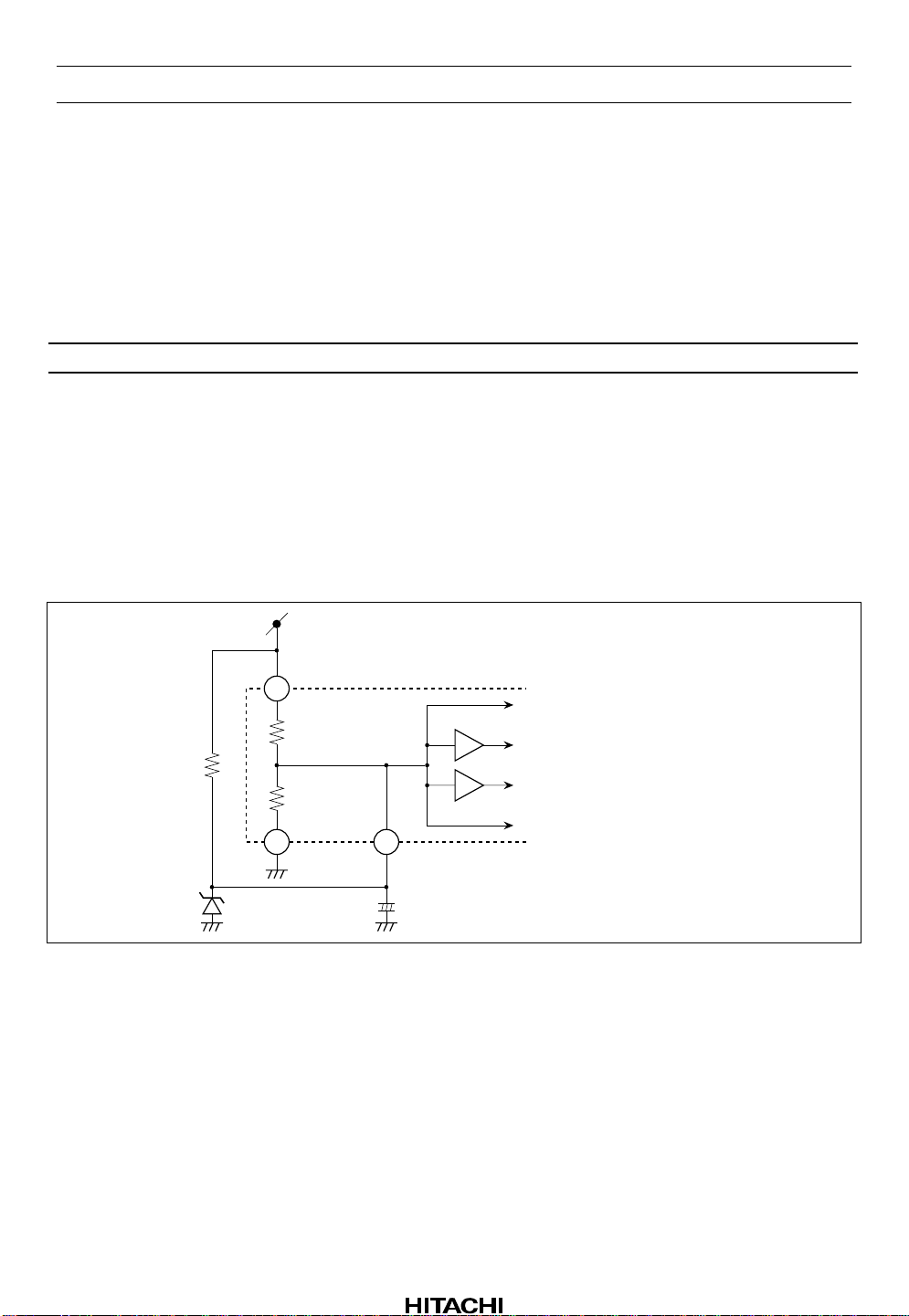
Pin Description, Equivalent Circuit (VCC = 12 V, Vref = 5.6 V, Ta = 25°C, No signal,
The value in the table show typical value.)
Pin No. Pin Name Note Equivalent Circuit Pin Description
1V
CC
V = V
CC
2 REC-OUT(L) V = Vref
3 REC-OUT(R)
4 REC-RETURN V = Vref
V’ = Vref
V
CC
GND
I
,
V4
5 pin, 6 pin
V
VCC pin
REC-EQ output
REC return
V
CC
I
GND
5 PB-IN B(L) PB B deck input
6 PB-IN B(R)
7VREF V = Vref
V’ = V
/ 2
CC
V
CC
Reference
10 k
,
V
V
10 k
GND
8 PB-IN A(L) V = Vref
V
CC
PB A deck input
PB-NF
9 PB-IN A(R)
Rev.2, Jul. 1998, page 2 of 29
Page 3
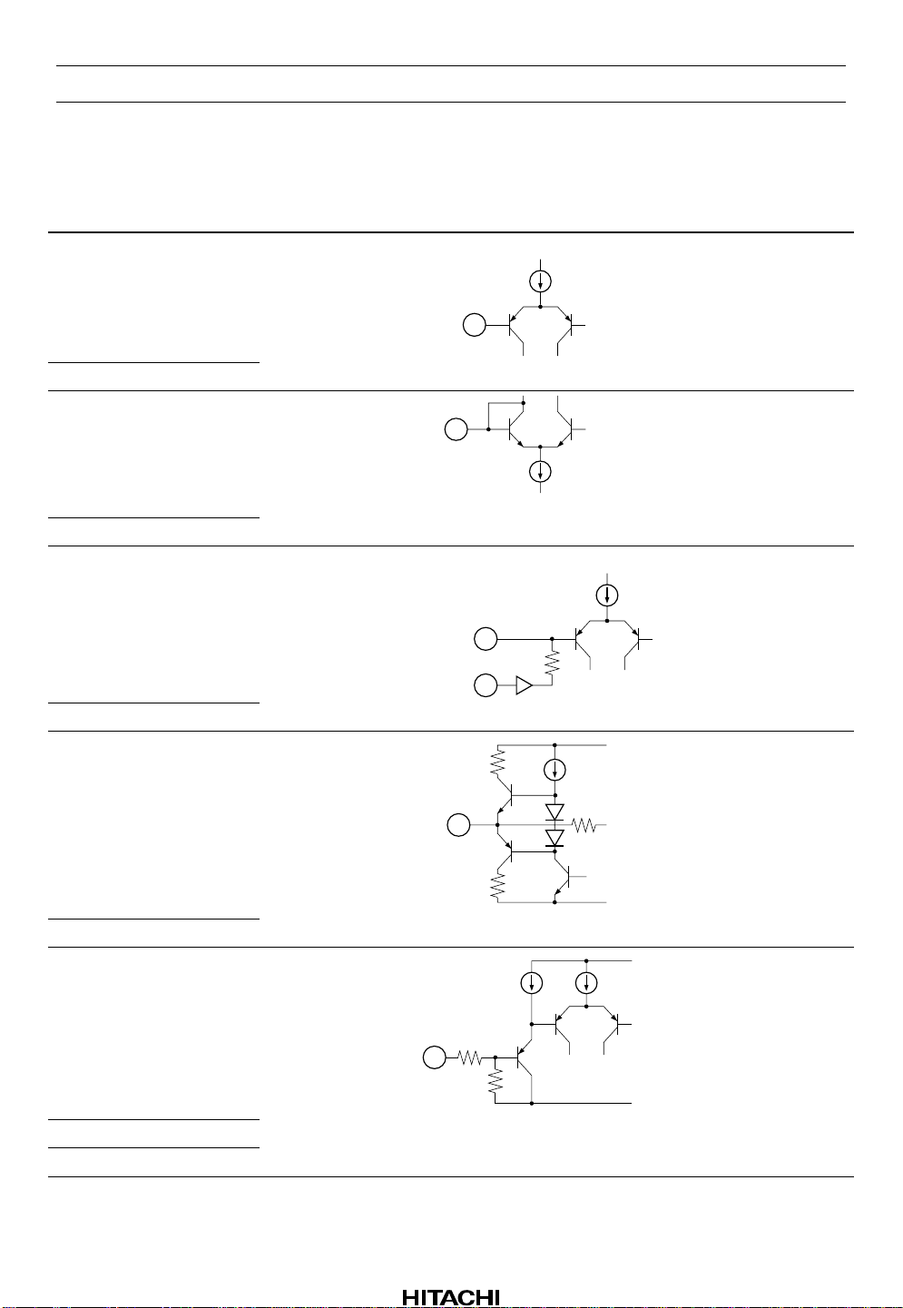
HA12219NT
Pin Description, Equivalent Circuit (VCC = 12 V, Vref = 5.6 V, Ta = 25°C, No signal,
The value in the table show typical value.) (cont)
Pin No. Pin Name Note Equivalent Circuit Pin Description
12 PB-NF(R) PB-IN = Vref
17 PB-NF(L)
13 PB-EQ(R) PB-OUT = Vref
16 PB-EQ(L)
21 REC-IN(R) V = Vref
V
CC
GND
PB-IN
PB-OUT
V
CC
PB-EQ feed back
NAB output
REC-EQ input
22 REC-IN(L)
14 PB-OUT(R) V = Vref
15 PB-OUT(L)
18 A 120/70 I = 20 µA
19 A/B
20 B I/
II
22k
100 k
7Vref
100 k
I
V
CC
GND
V
CC
GND
PB output
Mode control input
Rev.2, Jul. 1998, page 3 of 29
Page 4
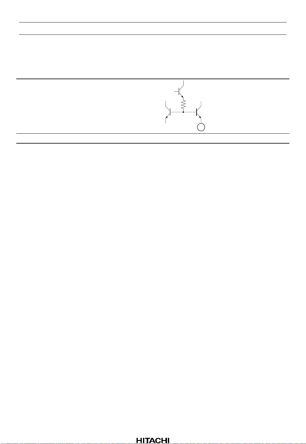
HA12219NT
Pin Description, Equivalent Circuit (VCC = 12 V, Vref = 5.6 V, Ta = 25°C, No signal,
The value in the table show typical value.) (cont)
Pin No. Pin Name Note Equivalent Circuit Pin Description
10 IREF V = 1.2 V
11 GND GND pin
Equalizer
reference current
input
Rev.2, Jul. 1998, page 4 of 29
Page 5
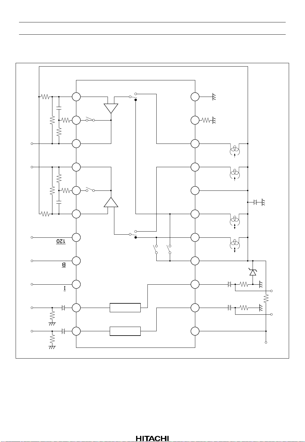
Block Diagram
HA12219NT
C : F
A /70
A/
13 12
14
17 16 15
18
−
120/70
PB-OUT(R)
PB-OUT(L)
120/70
−
AAB
+
B
GND
Unit R : Ω
IREF
10 11
PB-IN A(R)
PB-IN A(L)
VREF
+
+
PB-IN B(R)
5 6 7 8 9
Return SW
PB-IN B(L)
REC-RETURN
B
/II
20 19
+
(R)
21
+
(L)
22
(R)
REC-IN
(L)
REC-IN
REC-EQ
REC-EQ
(R)
(L)
REC-OUT
REC-OUT
CC
V
1 2 3 4
+ +
CC
V
Rev.2, Jul. 1998, page 5 of 29
Page 6

HA12219NT
Parallel Data Format
Pin No. Pin Name Lo Mid Hi
18 A 120/70 * — *
19 A/B B
Return SW OFF
REC Mute ON
20 B I/II REC-EQ *
TYPE I
Note: PB-EQ 120/70 logic
A/BBBB
A 120
120/70 B IIII/II Lo Mid Hi
120120
Lo Lo 120 µ 120 µ 120 µ
Lo Hi 70 µ 120 µ 120 µ
Hi Lo 120 µ 70 µ 70 µ
Hi Hi 70 µ 70 µ 70 µ
A
Return SW ON
REC Mute ON
—REC-EQ *
A
Return SW ON
REC Mute OFF
TYPE II
Rev.2, Jul. 1998, page 6 of 29
Page 7
HA12219NT
Functional Description
Power Supply Range
HA12219NT is designed to operate on single supply, shown by table 1.
Table 1 Supply Voltage
Item Power Supply Range
Single Supply 9.5 V to 15.0 V
Reference Voltage
As AC reference (Vref) of this IC has not a curr ent drivability, Vref fluctuates by A/B switching of PB-EQ.
Provided it causes you anxiety, please supply 7 pin with approximate 1/2 V
For example, a suitable circuit is shown by figure 1.
This IC has a capacitor charger for the Vref, indicated to the pin interface circuit figure.
voltage.
CC
470 Ω
V
CC
1
11
GND
7
Vref
+
470 µF
Figure 1 Reference Voltage Circuit
Lch PB-EQ Reference voltage
Lch REC-EQ Reference voltage
Rch REC-EQ Reference voltage
Rch PB-EQ Reference voltage
Rev.2, Jul. 1998, page 7 of 29
Page 8
HA12219NT
Operating Mode Control
HA12219NT provides fully electronic switching circuits. And each operating mode control is controlled
by parallel data (DC voltage).
Table 2 shows the control voltage of each control input pin.
Table 2 Control Voltage (Vth)
Pin No. Lo Mid Hi Unit Test Condition
18, 20 0.0 to 0.5 — 2.4 to V
CC
V
Input PinVMeasure
19 0.0 to 0.5 1.2 to 1.8 2.4 to V
CC
V
Note: 1. Each pin is pulled down with 100 kΩ internal resistor. 16 to 18 pins are low-level when each pin
is open.
2. Over shoot level and under shoot level of input signal must be the standardi ze d.
(High: Less than V
, Low: More than –0.2 V)
CC
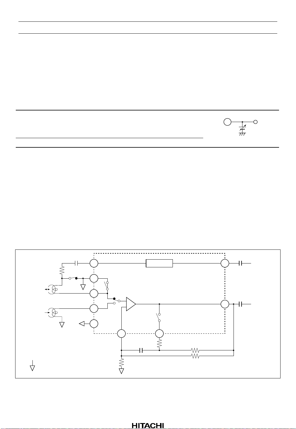
Block Diagram
Figure 2 shows the block diagram.
As this IC is built-in REC return switch, the configuration system can be simple system using a few
external component and the REC/PB head.
About these logics, please look at the Parallel Data Format.
REC-IN
22
PB-OUT
15
B head
A head
REC-OUT(L)
PB-IN B(L)
PB-IN A(L)
2
4
5
8
Return SW
B
+
−
A
REC - EQ
Vref
Rev.2, Jul. 1998, page 8 of 29
7
Figure 2 Block Diagram (Lch)
1310
Normal Speed
PB-A
Page 9
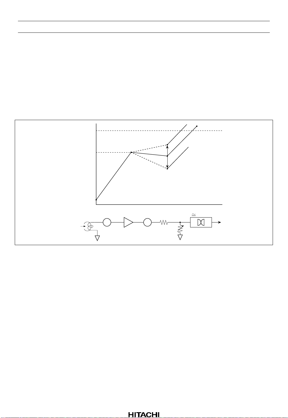
HA12219NT
Level Block Diagram
The gain establishment of PB-EQ considers PB output level
{(external AMP+PB AMP <HA12136A>) = 580 mV (Dolby Level)} like figure 3 as the target.
Regarding REC-EQ adjust the gain in front of input to this IC.
Similarly to PB, it consider Dolby level as a stan dard. And R1 needs the value more than 5.6 kΩ.
Because mode establishment resistances are built-in, REC-EQ frequ e n cy characteristics are respectiv ely
fixed value.
In case the change of the frequency characteristics are necessary, please inquire the responsible agent
because the adjustment of resistors is necessary.
580 mV
(Dolby level)
63.6 mV
HA12136A
0.6 mV
40.5 dB
PB-EQ
Figure 3 PB Level Block Diagram (120
Dolby IC
µµµµ
s, 1 kHz)
26 dB
Rev.2, Jul. 1998, page 9 of 29
Page 10

HA12219NT
Absolute Maximum Ratings (Ta = 25°C)
Item Symbol Rating Unit Note
Maximum supply voltage V
Power dissipation P
Operating temperature Topr –40 to +75 °C
Storage temperature Tstg –55 to +125 °C
Operating voltage Vopr 9.5 to 15 V
Note: HA12219NT operates on single supply voltage.
max 16 V
CC
T
500 mW Ta ≤ 75°C
Rev.2, Jul. 1998, page 10 of 29
Page 11

Electrical Characteristics (Ta = 25°C, VCC = 12 V, Vref = 5.6 V,
PBIN standard level = 0.6 mVrms at 1 kHz)
1
18, 201918, 20
2
Output
Input
RL
R L COM
Other
15
14
22
21
3
8
9
8/5 14 15
9/6
151515
141414
8/5
8/5
8/5
9/6
9/6
9/6
14 15
8/5
9/6
14 15
8/5
9/6
14 15
9/6
8/5
15
14
5
6
8
9
HA12219NT
No signal
Vin
fin
(mVrms)
(Hz)
Test Condition Application Terminal
70
/II A /70
I
B
IC Condition
A/
A
VVV
mA
0.5
32.7
23.1
−0.2
1.8
1.2
IQVILVIMVIHCT PB/REC(1)
REC-EQ → PB-EQ
PB-EQ → REC-EQ
1*1
*
0.6
1k1k1k
120
120
120
I
I
I
A/BAA/B
dBdBdBdBdB
CC
V
2.4
60.0
50.0
70.0
60.0
43.5
40.5
37.5
PB(1)
CT PB/REC(2)
G
0.6
10k
12070120
I
A/B
39.2
36.2
33.2
PB(2)
V
V
G
THD=1%
0.6
1k
10k
I
II
A/B
A/B
Vrms
35.0
0.6
32.0
0.3
29.0
PB(3)
V
G
Vomax PB
Rg=820Ω, DIN-AUDIO
1*1
*
0.6
1k1k
120
120
120
I
I
I
A/B
A/B
A/B
%
dB
µVrms
0.5
180.0
0.1
90.0
60.0
50.0
THD PB
VN PB
CT R/L(1)
1k
120
I
A
B
dB
70.0
60.0
CT A/B
Item Symbol Min Typ Max Unit
Quiescent current
Logical threshold
PB-REC crosstalk
PB-EQ gain
2
PB-EQ noise voltage
PB-EQ
PB-EQ THD
PB-EQ
maximum output *
= 9.5 V, Vref = 4.75 V
CC
2. V
channel separation
PB-EQ crosstalk
Note: 1. Large level without clipping
Rev.2, Jul. 1998, page 11 of 29
Page 12

HA12219NT
Electrical Characteristics (Ta = 25°C, VCC = 12 V, Vref = 5.6 V,
EQIN standard level = 20 dBs = 77.5 mVrms = 0 dB) (cont)
2
2
3
3
RLA/
Output
22 3 2
22
22
Input
R L COM
212121
Other
Vin
7.75
7.75
1k
5k
7.75
12.5k
(mVrms)
fin
(Hz)
Test Condition Application Terminal
120
120
120
I
I
I
B /II A /70
IC Condition
AAAAAAA
dBdBdBdBdBdBdB
222
333
22
22
22
212121
7.75
7.75
7.75
1k
5k
12.5k
120
120
120
IIIIII
32
22
21
1*1
*
1k
120
I
32
22
21
1k
120
I
MID
dB
2
32
3
22
22
21
21
THD=1%
77.5
1k
1k
120
120
I
I
A
AREC-EQ THD
%
Vrms
I
AS/N REC 61.0 64.0 dB 120 1k 21 22 3 2REC-EQ S/N Rg=5.1kΩ, A-WTG
21.5
23.4
35.1
25.3
28.7
39.6
20.0
21.4
32.1
23.8
26.7
36.6
18.5
19.4
29.1
22.3
24.7
33.6
REC-NN1
REC-NN2
REC-NN3
REC-NC1
REC-NC2
V
V
V
G
G
G
V
G
REC-NC3
V
V
G
G
Item Symbol Min Typ Max Unit
REC-EQ frequency
response
TYPE I
REC-EQ frequency
response
TYPE II
Rev.2, Jul. 1998, page 12 of 29
70.0
61.0
CT R/L(2)
REC-EQ
channel separation
1.8
76.0
1.2
66.0
R-MUTE ATT
Vomax REC
2
REC-MUTE
attenuation
REC-EQ
maximum output *
0.5
0.2
THD REC
= 9.5 V, Vref = 4.75 V
CC
2. V
Note: 1. Large level without clipping
Page 13

Test Circuit
Noise
meter
Oscilo
scope
HA12219NT
R12
R13
10k
10k
Rch
Lch
SW3
SW11
Lch
Rch
C10
C11
analyzer
SW12
PB
PB-NF(R)
+
R8
180
C9
0.01µ
SW10
SW9
SW8
R10
R11
R14
R16
C12
C13
+
18k
12k
12k
18k
0.01µ
13 12
14
17 16 15
18
20 19
0.47µ
R9
330k
+
2.2µ
+
2.2µ
R15
330k
R17
180
12070
BA
A
III
21
R18
5.1k
C14
0.47µ
+
22
R19
5.1k
−
120/70
PB-EQ(R)
PB-OUT(R)
PB-OUT(L)
120/70
PB-EQ(L)
−
+
PB-NF(L)
A /70
A/
/II
B
(R)
REC-IN
(R)
(L)
REC-IN
(L)
REC
A
B
A
B
REC-EQ
REC-EQ
AC-VM2
Return SW
(R)
(L)
GND
11
R7
IREF
PB-IN A(R)
PB-IN A(L)
VREF
PB-IN B(R)
5 6 7 8 9 10
PB-IN B(L)
+ + + +
REC-RETURN
REC-OUT
C3
+ +
REC-OUT
C2
CC
V
1 2 3 4
+
C1
22k
Vref
DC
source 4
R6
820
C8
22µ
R5
820
C7
22µ
C6
470µ
+
R4
820
C5
22µ
R3
820
C4
22µ
R2
10k
SW7
2.2µ
2.2µ
100µ
Rch
R1
10k
DC
source 1
DC
source 2
Lch
V
Lch
CC
Rch
SW5
Bin
SW4
Unit R : Ω
Lch
Rch
SW6
Ain
Distortion
C : F
REC
SW2
DC
PB
OFFON
Audio-SGAC-VM1
SW1
source 3
Rev.2, Jul. 1998, page 13 of 29
Page 14

HA12219NT
Characteristic Curves
25
20
(mA)
Q
15
Quiescent Current I
Quiescent Current vs. Supply Voltage
BI
BII
A 120
A 70
10
70
60
50
40
PB-EQ Gain (dB)
30
Ain
→ PBOUT
Bin
VCC = 8V, 12V, 16V
20
10
8
10 12 14
Supply Voltage (V)
PB-EQ Gain vs. Frequency
120µ
70µ
100 1k 10k 100k
Frequency (Hz)
16
Rev.2, Jul. 1998, page 14 of 29
Page 15

PB-EQ Maximum Output Level vs. Supply Voltage (1)
5
Ain, PBOUT, NN
100Hz
1kHz
10kHz
4
3
2
Maximum Output Level Vomax (Vrms)
1
8
10 12 14
Supply Voltage (V)
HA12219NT
16
PB-EQ Maximum Output Level vs. Supply Voltage (2)
5
Ain, PBOUT, NC
100Hz
1kHz
10kHz
4
3
2
Maximum Output Level Vomax (Vrms)
1
8
10 12 14
Supply Voltage (V)
16
Rev.2, Jul. 1998, page 15 of 29
Page 16

HA12219NT
PB-EQ Total Harmonic Distortion vs. Output Level (1)
Ain
PBOUT
Bin
VCC = 12V, Vref = 5.6V
NN
1.0
0.1
Total Harmonic Distortion T.H.D. (%)
0.01
100Hz
1kHz
10kHz
−20
Output Level Vout (dBs)
PB-EQ Total Harmonic Distortion vs. Output Level (2)
Ain
PBOUT
Bin
VCC = 12V, Vref = 5.6V
NC
1.0
0.1
Total Harmonic Distortion T.H.D. (%)
0.01
−20
100Hz
1kHz
10kHz
Output Level Vout (dBs)
010−10
010−10
20
20
Rev.2, Jul. 1998, page 16 of 29
Page 17

180
170
160
150
140
130
120
110
100
Noise (µVrms)
90
80
70
60
50
Ain
Vref = 1/2V
wait DIN/AUDIO
Rch 120µ
Rch 70µ
Lch 120µ
Lch 70µ
81513119
PB-EQ Noise Level vs. Supply Voltage (1)
CC
10 12 14
Supply Voltage (V)
HA12219NT
16
180
170
160
150
140
130
120
110
100
Noise (µVrms)
90
80
70
60
50
Bin
Vref = 1/2V
wait DIN/AUDIO
Rch 120µ
Rch 70µ
Lch 120µ
Lch 70µ
81513119
PB-EQ Noise Level vs. Supply Voltage (2)
CC
10 12 14
Supply Voltage (V)
16
Rev.2, Jul. 1998, page 17 of 29
Page 18

HA12219NT
45
39
33
27
REC-EQ Gain (dB)
21
15
100 1k 10k 100k
Rin → RECOUT
Vin = 7.75mVrms
V
= 12V, Vref = 5.6V
CC
REC-EQ Gain vs. Frequency
NC
NN
Frequency (Hz)
REC-EQ Maximum Output Level vs. Supply Voltage (1)
5
NN
100Hz
1kHz
10kHz
4
3
2
Maximum Output Level Vomax (Vrms)
1
8
10 12 14
Supply Voltage (V)
16
Rev.2, Jul. 1998, page 18 of 29
Page 19

REC-EQ Maximum Output Level vs. Supply Voltage (2)
5
NC
100Hz
1kHz
10kHz
4
3
2
Maximum Output Level Vomax (Vrms)
1
8
10 12 14
Supply Voltage (V)
HA12219NT
16
REC-EQ Total Harmonic Distortion vs. Output Level (1)
100
Rin → RECOUT
NN
V
= 12V, Vref = 5.6V
CC
100Hz
1kHz
10kHz
10
1.0
Total Harmonic Distortion T.H.D. (%)
0.1
−20
Output Level Vout (dBs)
100−10
20
Rev.2, Jul. 1998, page 19 of 29
Page 20

HA12219NT
REC-EQ Total Harmonic Distortion vs. Output Level (2)
100
Rin → RECOUT
NC
V
= 12V, Vref = 5.6V
CC
100Hz
1kHz
10kHz
10
1.0
Total Harmonic Distortion T.H.D. (%)
0.1
−20
Output Level Vout (dBs)
100−10
20
REC-EQ Signal to Noise Ratio vs. Supply Voltage
70
RECOUT
A-WTG filter
NN
NC
65
60
Signal to Noise Ratio S/N (dB)
55
8
10 12 14
Supply Voltage (V)
16
Rev.2, Jul. 1998, page 20 of 29
Page 21

PB-EQ Channel Separation vs. Frequency (L ↔ R) (1)
−30
Ain → PBOUT
Vin = +12dB
V
= 12V, Vref = 5.6V
CC
L ↔ R
−40
−50
−60
Channel Separation (dB)
−70
HA12219NT
NC
NN
−80
PB-EQ Channel Separation vs. Frequency (L ↔ R) (2)
−30
Bin → PBOUT
Vin = +12dB
V
= 12V, Vref = 5.6V
CC
L ↔ R
−40
−50
−60
Channel Separation (dB)
−70
−80
10010 1k 10k 100k
Frequency (Hz)
NN
NC
10010 1k 10k 100k
Frequency (Hz)
Rev.2, Jul. 1998, page 21 of 29
Page 22

HA12219NT
−20
−40
−60
−80
Crosstalk (dB)
−100
Ain → Bin
Vin = +12dB
V
= 12V, Vref = 5.6V
CC
NN, NC
PB-EQ Crosstalk vs. Frequency (Input: Ain → Bin)
−120
−20
Bin → Ain
Vin = +12dB
V
= 12V, Vref = 5.6V
CC
NN, NC
−40
−60
−80
Crosstalk (dB)
−100
−120
10010 1k 10k 100k
Frequency (Hz)
PB-EQ Crosstalk vs. Frequency (Input: Bin → Ain)
10010 1k 10k 100k
Frequency (Hz)
Rev.2, Jul. 1998, page 22 of 29
Page 23

0
RECOUT
Vin = 100mVrms
V
CC
−10
+
−20
Ripple Rejection Ratio vs. Frequency (REC)
= 12V, Vref = 5.6V
1
51Ω
V
CC
+
470µ
Vref
7
470Ω470Ω
11
HA12219NT
NC
−30
Ripple Rejection Ratio R.R.R. (dB)
−40
−50
10010 1k 10k 100k
Ripple Rejection Ratio vs. Frequency (PB)
0
PBOUT
Vin = 100mVrms
V
= 12V, Vref = 5.6V
CC
−20
−40
1
+
51Ω
V
CC
+
470µ
Vref
7
470Ω470Ω
−60
NN
Frequency (Hz)
11
NN
NC
Ripple Rejection Ratio R.R.R. (dB)
−80
−100
10010 1k 10k 100k
Frequency (Hz)
Rev.2, Jul. 1998, page 23 of 29
Page 24

HA12219NT
−40
−60
−80
−100
Mute Attenuation (dB)
−120
Rin → RECOUT
Vin = +12dB
V
= 12V, Vref = 5.6V
CC
Mute Attenuation vs. Frequency
NN
NC
−140
REC-EQ Channel Separation vs. Frequency (R → L)
−20
Rin → RECOUT
Vin = +12dB
V
= 12V, Vref = 5.6V
CC
Rch → Lch
−40
−60
−80
Channel Separation (dB)
−100
−120
10010 1k 10k 100k
Frequency (Hz)
NC
NN
10010 1k 10k 100k
Frequency (Hz)
Rev.2, Jul. 1998, page 24 of 29
Page 25

−20
Rin → RECOUT
Vin = +12dB
V
CC
Lch → Rch
−40
HA12219NT
REC-EQ Channel Separation vs. Frequency (L → R)
= 12V, Vref = 5.6V
NC
−60
−80
Channel Separation (dB)
−100
−120
Crosstalk vs. Frequency (Mode: REC-EQ → PB-EQ)
−20
Rin → PBOUT
Vin = 60mVrms
V
= 12V, Vref = 5.6V
CC
−40
−60
NN
10010 1k 10k 100k
Frequency (Hz)
NC
−80
Crosstalk (dB)
−100
−120
NN
10010 1k 10k 100k
Frequency (Hz)
Rev.2, Jul. 1998, page 25 of 29
Page 26

HA12219NT
0
−20
−40
−60
Crosstalk (dB)
Crosstalk vs. Frequency (Mode: PB-EQ → REC-EQ) (1)
Ain → RECOUT
Vin = +15dB
V
= 12V, Vref = 5.6V
CC
A70
−80
−100
−20
Bin → RECOUT
Vin = +15dB
V
= 12V, Vref = 5.6V
CC
−40
−60
−80
Crosstalk (dB)
A120
10010 1k 10k 100k
Frequency (Hz)
Crosstalk vs. Frequency (Mode: PB-EQ → REC-EQ) (2)
BI
BII
−100
−120
Rev.2, Jul. 1998, page 26 of 29
10010 1k 10k 100k
Frequency (Hz)
Page 27

Altered Reference Voltage vs. External Resistance
400
300
V
V
CC
1
R21
CC
R22
VCC = 12V (Vref = 1/2 VCC)
Vref
7
200
∆Vref (PB-A vs. PB-B) (mV)
100
0
100 1k 100k10k 1M
Resistance (Ω) (R21, R22 same)
HA12219NT
−23
−24
−25
−26
RETURN Level (dB)
−27
−28
10
RETURN Level vs. Frequency
Pin 5 or 6
4
Vref
Vout
820Ω
+
22µ
Vin
V
Vin = 1Vrms
Vin = 800mVrms
Vin = 600mVrms
Vin = 400mVrms
100 1k 10k 100k
Frequency (Hz)
Rev.2, Jul. 1998, page 27 of 29
Page 28

HA12219NT
Package Dimensions
22
Unit: mm
19.2
20.32 Max
12
6.3
1
0.89
1.17 Max
1.78 ± 0.25
1.0
0.48 ± 0.10
11
7.4 Max
0.51 Min
2.90 Min 5.06 Max
Hitachi Code
JEDEC
EIAJ
Weight
7.62
+ 0.10
0.25
Ð 0.05
0¡ Ð 15¡
(reference value)
DP-22NS
Ñ
Conforms
0.90 g
Rev.2, Jul. 1998, page 28 of 29
Page 29

HA12219NT
Disclaimer
1. Hitachi neither warrants nor grants licenses of any rights of Hitachi’s or any third party’s patent,
copyright, trademark, or other intellectual property rights for information contained in this document.
Hitachi bears no responsibility for problems that may arise with third party’s rights, including
intellectual property rights, in connection with u se of the information contained in this document.
2. Products and product specifications may be subject to change without notice. Confirm that you have
received the latest product standards or specifications before final design, purchase or use.
3. Hitachi makes every attempt to ensure that its products are of high quality and reliability. However,
contact Hitachi’s sales office before using the product in an application that demands especially high
quality and reliability or where its failure or malfunction may directly threaten human life or cause risk
of bodily injury, such as aerospace, aeronautics, nuclear power, combustion control, transportation,
traffic, safety equipment or medical equipment for life support.
4. Design your application so that the product is used within the ranges guaranteed by Hitachi particularly
for maximum rating, operating supply voltage range, heat radiation characteristics, installation
conditions and other characteristics. Hitachi bears no responsibility for failure or damage when used
beyond the guaranteed ranges. Even within the guaranteed ranges, consider normally foreseeable
failure rates or failure modes in semiconductor devices and employ systemic measures such as failsafes, so that the equipment incorporating Hitachi product does not cause bodily injury, fire or other
consequential damage due to operation of the Hitachi product.
5. This product is not designed to be radiation resistant.
6. No one is permitted to reproduce or duplicate, in any form, the whole or part of this document without
written approval from Hitachi.
7. Contact Hitachi’s sales office for any questions regarding this document or Hitachi semiconductor
products.
Sales Offices
Hitachi, Ltd.
Semiconductor & Integrated Circuits.
Nippon Bldg., 2-6-2, Ohte-machi, Chiyoda-ku, Tokyo 100-0004, Japan
Tel: Tokyo (03) 3270-2111 Fax: (03) 3270-5109
URL NorthAmerica : http://semiconductor.hitachi.com/
For further information write to:
Hitachi Semiconductor
(America) Inc.
179 East Tasman Drive,
San Jose,CA 95134
Tel: <1> (408) 433-1990
Fax: <1>(408) 433-0223
Europe : http://www.hitachi-eu.com/hel/ecg
Asia : http://sicapac.hitachi-asia.com
Japan : http://www.hitachi.co.jp/Sicd/indx.htm
Hitachi Europe GmbH
Electronic Components Group
Dornacher Straße 3
D-85622 Feldkirchen, Munich
Germany
Tel: <49> (89) 9 9180-0
Fax: <49> (89) 9 29 30 00
Hitachi Europe Ltd.
Electronic Components Group.
Whitebrook Park
Lower Cookham Road
Maidenhead
Berkshire SL6 8YA, United Kingdom
Tel: <44> (1628) 585000
Fax: <44> (1628) 585160
Hitachi Asia Ltd.
Hitachi Tower
16 Collyer Quay #20-00,
Singapore 049318
Tel : <65>-538-6533/538-8577
Fax : <65>-538-6933/538-3877
URL : http://www.hitachi.com.sg
Hitachi Asia Ltd.
(Taipei Branch Office)
4/F, No. 167, Tun Hwa North Road,
Hung-Kuo Building,
Taipei (105), Taiwan
Tel : <886>-(2)-2718-3666
Fax : <886>-(2)-2718-8180
Telex : 23222 HAS-TP
URL : http://www.hitachi.com.tw
Hitachi Asia (Hong Kong) Ltd.
Group III (Electronic Components)
7/F., North Tower,
World Finance Centre,
Harbour City, Canton Road
Tsim Sha Tsui, Kowloon,
Hong Kong
Tel : <852>-(2)-735-9218
Fax : <852>-(2)-730-0281
URL : http://www.hitachi.com.hk
Copyright Hitachi, Ltd., 2000. All rights reserved. Printed in Japan.
Colophon 2.0
Rev.2, Jul. 1998, page 29 of 29
 Loading...