

Page 1

HA12211NT
Audio Signal Processor for Cassette Deck (Deck 1 Chip)
ADE-207-223A (Z)
2nd. Edition
June 1997
Description
HA12211NT is silicon monolithic bipolar IC providing REC equalizer system, PB equalizer system and
each electronic control switch in one chip.
Functions
• PB equalizer × 2 channel
• REC equalizer × 2 channel
• Each electronical control switch to change equalizer characteristics
• REC mute
• REC head return switch
Features
• REC equalizer is very small numb er of external parts.(4 types of frequency characteristics built-in )
• PB equalizer built-in. (A/B input changing system, 4 types of frequency characteristics)
• Independent PB sensitivity for A d eck, B d eck.
• Normal-speed/high-speed, normal tape/chr ome tape switching built-in.
• Controllable from direct micro-computer output.
• Available to reduce substrate-area because of high integration and small external parts.
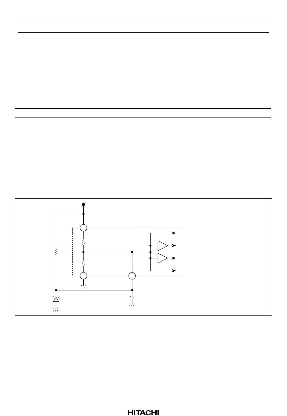
Page 2
HA12211NT
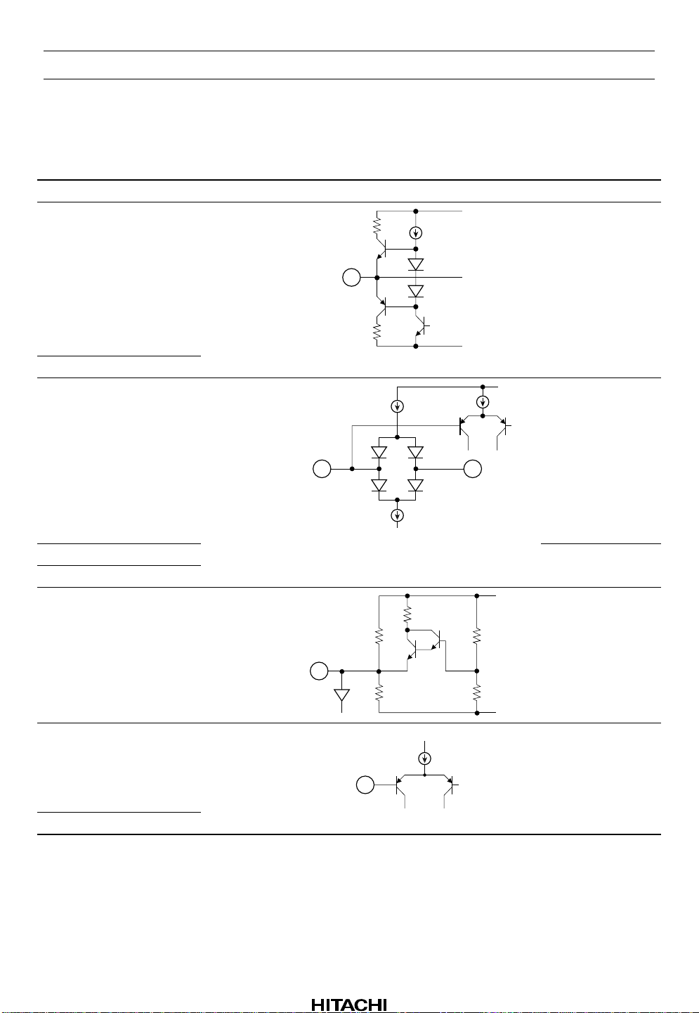
Pin Description, Equivalent Circuit (VCC = 10.5V, Vref = 5.25V, Ta = 25°C, No signal,
The value in the table show typical value.)
Pin No. Pin Name Note Equivalent Circuit Pin Description
1V
CC
V = V
CC
2 RECOUT (L) V = Vref
3RECOUT (R)
4 REC-RETURN V = Vref
V’ = Vref
V
CC
V
GND
V
I
CC
VCC Pin
REC-EQ output
REC Return
V4
5 pin, 6 pin
I
GND
V’
5 PB-IN B (L) PB B Deck input
6 PB-IN B (R)
7VREF V = Vref
V’ = V
/ 2
CC
8 PB-IN A(L) V = Vref
10k
V
10k
V
CC
V
CC
V’
GND
Reference
PB A Deck input
V
9 PB-IN A(R)
Rev.2, Jun. 1997, page 2 of 34
Page 3
HA12211NT
Pin Description, Equivalent Circuit (VCC = 10.5V, Vref = 5.25V, Ta = 25°C, No signal,
The value in the table show typical value.) (cont)
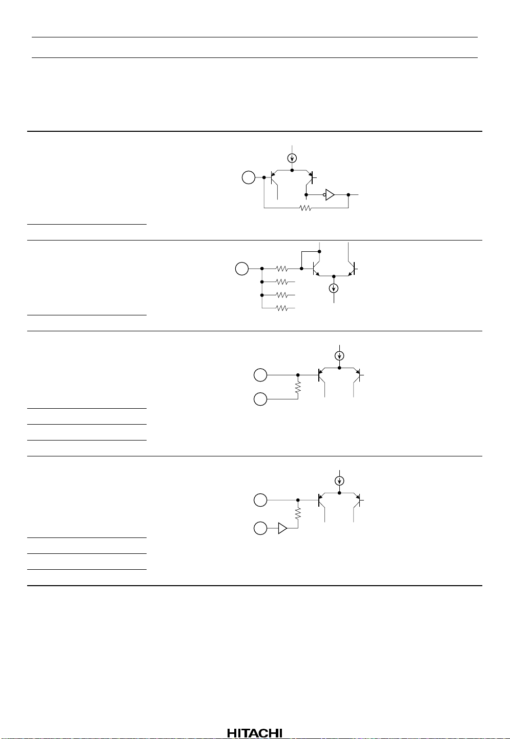
Pin No. Pin Name Note Equivalent Circuit Pin Description
10 PB-NF (L) V = Vref
11 PB-NF (R)
12 PB-EQ (L) V = Vref
13 PB-EQ (R)
14 PB-Cal A(L) V = Vref
V
CC
V
139k
V
GND
V
CC
PB EQ Feed back
NAB Output
Feed back input
for gain
adjustment
15 PB-Cal A(R)
16 PB-Cal B(R)
17 PB-Cal B(L)
26 AUX (R) V = Vref
27 AUX (L)
28 TAPE (R)
29 TAPE (L)
10k
7Vref V
100k
7Vref V
V
CC
REC-EQ input
Rev.2, Jun. 1997, page 3 of 34
Page 4
HA12211NT
Pin Description, Equivalent Circuit (VCC = 10.5V, Vref = 5.25V, Ta = 25°C, No signal,
The value in the table show typical value.) (cont)
Pin No. Pin Name Note Equivalent Circuit Pin Description
18 PBOUT (R) V = Vref
19 PBOUT (L)
20 A/B I = 20µA
21 HSP
22 Acr
23 Bcr
24 REC-SEL I = 20µA
V = 2.5V
V
CC
V
GND
V
CC
I
22k
100k
GND
V
I
CC
PB output
Mode control input
Mode control input
100k
25 IREF V = 1.2V
V
50k
GND
Equalizer
reference current
input
V
30 GND GND Pin
Rev.2, Jun. 1997, page 4 of 34
Page 5
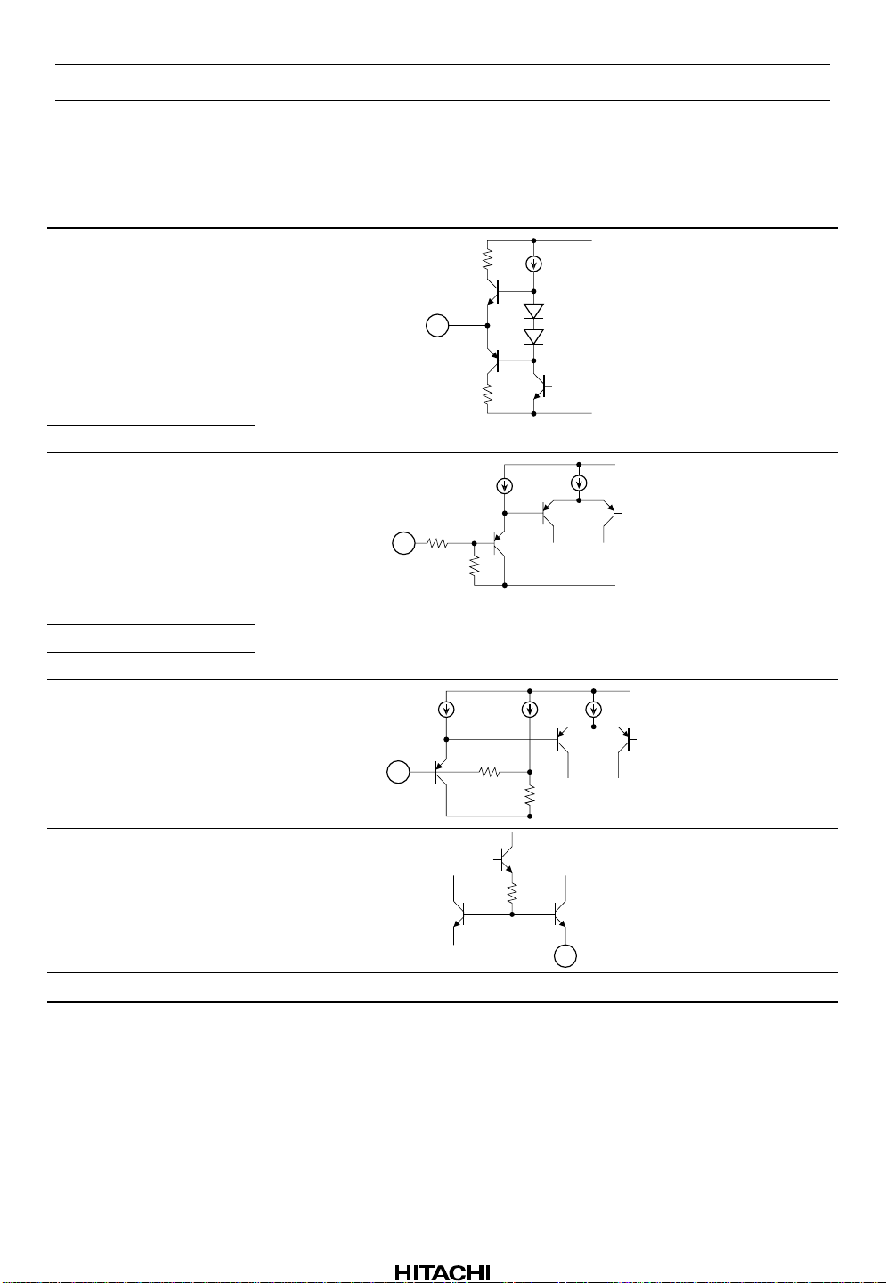
Block Diagram
CC
GND
V
HA12211NT
to Dolby
REC IN from logic
)
: 100kB
R
(L)
(R)
(L)
R
(L)
B
A/B
HSP
ACr
BCr
IREF
AUX
AUX
TAPE(
TAPE
)
R
(
B
)
L
(
B
(R)
PB-OUT
PB-OUT
19 18 17 16
21 20
22
REC-SEL
30 29 28 27 26 25 24 23
GND
PB-CAL
PB-CAL
L-ch
12dB
R-ch
B
: 100kB
B
PB-CAL
PB-CAL
–
+
10k
A
B
12 13 14 15
PB-EQ PB-EQ
PB-NF
10 11
9
5k 2.7k 2.26k 1.12k
–
+
139k
PB-IN PB-IN PB-NF
A
REC-EQ
PB-IN PB-IN
REC-RETURN
R
)
R
(
A
)
L
(
A
)
R
)(
L
(
0.022µ
)
R
(
0.022µ
)
L
470 470
)(
R
(
A
)
L
(
A
VREF
)
R
(
B
)
L
(
B
C : F
Unit R : Ω
470µ
+
R-ch
REC-OUT
(R)
470
Bias
470
L-ch
REC-OUT
(L)
5.6k 5.6k
CC
12345678
V
Rev.2, Jun. 1997, page 5 of 34
Page 6

HA12211NT
Parallel Data Format
Pin No. Pin Name L M H
22 A CrO2 *
23 B CrO2 *
1, *3
1, *2, *3
21 HSP Normal speed *
20 A/B Ain active *
1, *3
Return SW ON *
REC OUT active *3—REC OUT Hiz
24 REC IN SEL TAPE MUTE *
Note: 1. PB-EQ LOGIC
HSP
LH
A/B
A CrO2 B CrO2 L H L H
L L 120µ 120µ 60µ 60µ
L H 120µ 70µ 60µ 35µ
HL70µ 120µ 35µ 60µ
HH70µ 70µ 35µ 35µ
—*
—*
3
—Hi speed
— Bin active *
3
— Return SW OFF
3
1
1, *2
1
AUX
2. REC-EQ LOGIC
HSP
B CrO2 L H
L Normal speed
TAPE I
H Normal speed
II
TAPE
3. Unforced pin state
High speed
TAPE I
High speed
II
TAPE
Rev.2, Jun. 1997, page 6 of 34
Page 7
HA12211NT
Functional Description
Power Supply Range
This IC is designed to operate on single supply, shown by table 1.
Table 1 Spply Voltage
Item Power Supply Range
Single Supply 9.5V to 15.0V
Reference Voltage
So little is the current drivability of AC refer ence (Vr ef) that the Vref voltage may be altered by A/B
switching of PB-EQ.
Provided it causes you anxiety, please use the constant 1/2 V
In addition, this IC has a capacitor charger for Vref pin.
V
CC
1
470Ω
30
GND
7
Vref
+
470µF
Figure 1 Reference Voltage Circuit
voltage circuit, for example, figure 1.
CC
Lch PB-EQ reference voltage
Lch REC-EQ reference voltage
Rch REC-EQ reference voltage
Rch PB-EQ reference voltage
Rev.2, Jun. 1997, page 7 of 34
Page 8
HA12211NT
Operating Mode Control
This IC provides fully electronic switching circuits. And each operating mode control is controlled by
parallel data (DC voltage).
Table 2 Threshold Voltage (Vth)
Pin No. Lo Mid Hi Unit Test Condition
20, 21, 22, 23 0.0 to 2.5 — 4.0 to V
CC
V
Input Pin Measure
V
24 0.0 to 1.0 2.0 to 3.0 4.0 to V
CC
V
Note: 1. 20 to 23 pins are pulled down Lo level, and 24 pin is pulled to Mid level by the inside resistor
100kΩ.
2. Over shoot level and under shoot level of input signal must be the standardi ze d.
(High: V
, Low: –0.2V)
CC
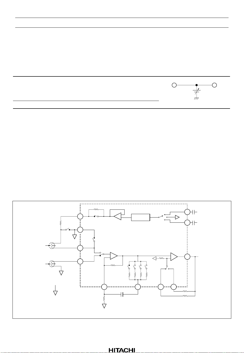
Block Diagram
This IC can be constructed for simple system which has little external parts by used the head serving both
as Recording and Play back because of REC return SW built-in.
With output Hi-Z of REC-EQ and input muting, this IC is realized not only REC mute attenuation
sufficiently but reducing pop noise in REC muting.
Note: Referring to Parallel Data Format also.
C9
Tape IN
29
C11
AUX IN
27
19
PBOUT
+
–
B head
A head
RECOUT
R1
PB IN (B)
PB IN (A)
2
4
5
8
Hi-Z SW
RETURN SW
B
A
–
REC - EQ
+
+
–
Vref
Rev.2, Jun. 1997, page 8 of 34
10 12
R7 C7
Figure 2 Block Diagram (Lch)
14
17
Normal Speed
Normal Tape
PB - A, Tape IN Select
R18
R9
Page 9
HA12211NT
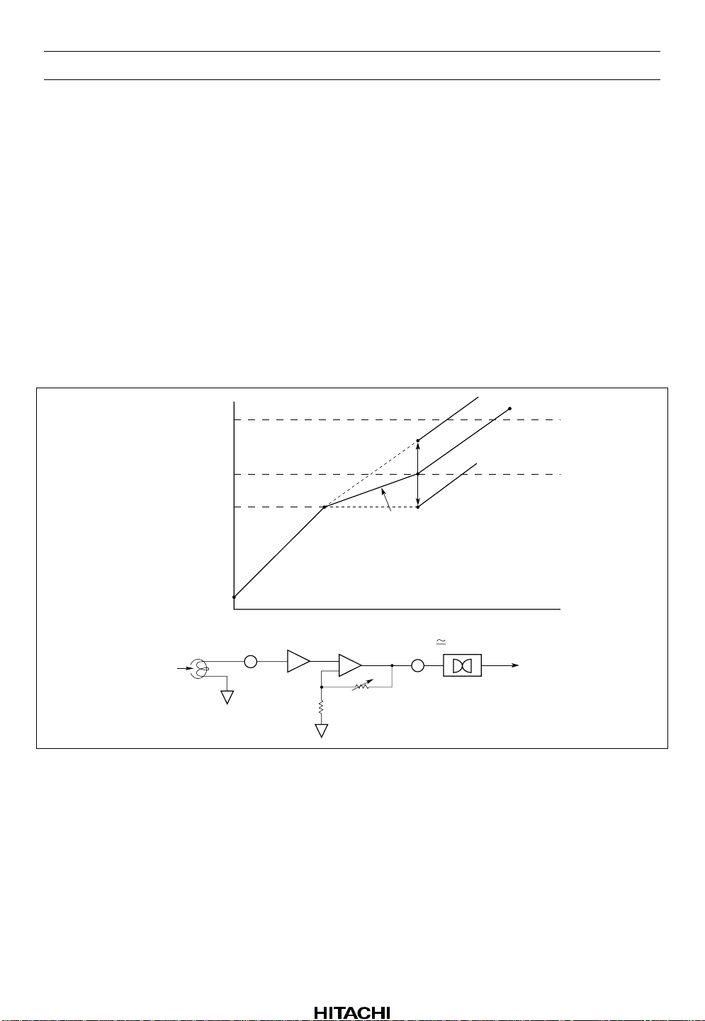
Level Diagram
It is the target that total play back output level is adjusted to 3 00mV; Dolby level, which the PB system
gain in all is included of external amplifier’s (Dolby IC etc.) as follows figure 3. Though A head
adjustment is independent of B, select the value of R9, R18 adequately.
Regarding REC-EQ adjust the gain in front of input to this IC.
The level diagram at 1kHz is shown by figure 4.
Note: 1. R1 needs the valu e mor e than 1kHz.
2. Depending on the employed REC/PB head and test tape characteristics, there is rare case that
the REC-EQ frequency characteristics of this IC can not be matched to the required
characteristics because of built-in resistors which determined the REC-EQ parameters in this
case, please inquire the responsible agent because of the adjustment of built-in resistors is
necessary.
300mV
(Dolby Level)
23.9mV
HA12134A
11.3mV
0.6mV
100kΩ
25.5dB 0 to 20.8dB 20dB
+
–
10kΩ
100kΩ VR
VR = 11kΩ
Dolby IC
Figure 3 PB Level Diagram (Normal Speed, Normal Tape, 1kHz)
Rev.2, Jun. 1997, page 9 of 34
Page 10
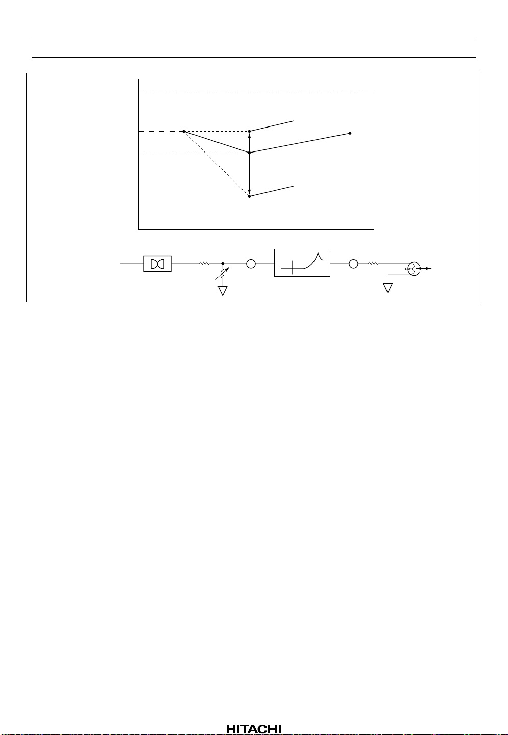
HA12211NT
REC-EQ clip level
1.8V
300mV
(Dolby Level)
100mV
1kHz
Dolby IC
263mV
REC-EQ
Figure 4 REC Level Diagram (Normal Speed, Normal Tape, 1kHz)
5.6kΩ
R1
Rev.2, Jun. 1997, page 10 of 34
Page 11

HA12211NT
Absolute Maximum Rating (Ta = 25°C)
Item Symbol Rating Unit Note
Max supply voltage V
Power dissipation P
Operating temperature Topr –40 to +75 °C
Storage temperature Tstg –55 to +125 °C
Operating voltage Vopr 9.5 to 15 V
max 16 V
CC
d
500 mW Ta ≤ 75°C
Rev.2, Jun. 1997, page 11 of 34
Page 12

HA12211NT
Electrical Characteristics (Ta = 25°C, VCC = 10.5V, Vref = 5.25V, PB-EQ standard DC
gain 55.9dB (R9, R10, R18, R19 = 11.0kΩ))
1
COM
20 to2324
24
20 to
24
Application Terminal
Input Output
RRLL
Other
No signal
19
18
26/
27/
19
18
8/5
9/6
18
8/5
9/6
19
18
8/5
9/6
1818181818
8/5
8/5
8/5
9/6
9/6
9/6
2
3
8
28
9
29
1919191919
19
THD=1%*2Rg=820Ω, DIN-AUDIO
8/5
9/6
19
18
8/5
9/6108
9/6
8/5119
19
18
Vin
—
(mVrms)
fin
(Hz)
—
REC
IN SEL
Mute
B CrO2
TYPE I
A CrO2
TYPE I
HSP
Norm
IC Condition
A/B
Test Condition
AQuiescent current
mAVV
32.0
22.8——
Min Typ Max Unit
16.0
Q
I
—
—
—
—
—
—
—
2.5
–0.2
1
V
—
—
—
—
—
—
—
—
—
—
—
—
—
—
—
—
—
—
—
—
—
V
V
CC
1.0
3.0
V
—
—
–0.2
2.0
4.0
2
IL
IM
IL
VIHV
V
1
1k
AUX
Tape/
AUX
TYPE I
TYPE I
Norm
A
dB
—
70
60
CT PB/REC(2)
0.6
1k
Tape
TYPE I
TYPE I
Norm
A/B
dBdBdBdBdB
35.0
32.0
29.0
PB (1)
V
G
*1*
1k
Tape/
TYPE I
TYPE I
Norm
A/B
dB
—
60
50
CT PB/REC(1)
0.6
0.6
10k
10k
Tape
Tape
TYPE I
TYPE II
TYPE I
TYPE II
Norm
Norm
A/B
A/B
31.0
26.8
28.0
23.8
25.0
20.8
PB (3)
PB (2)
V
V
G
G
0.6
0.6—0.6
20k
20k1k1k
Tape
Tape
TYPE I
TYPE II
TYPE I
TYPE II
High
High
A/B
A/B
25.4
20.8—0.5
22.4
17.8
19.4
14.8
PB (4)
PB (5)
V
V
G
G
Tape
Tape
TYPE I
TYPE I
TYPE I
TYPE I
Norm
Norm
A/B
A/B
Vrms
%
2.0
0.1
0.3
—
Vomax PB
THD PB
1
—
*1*
—
1k
1k
Tape
Tape
Tape
TYPE I
TYPE I
TYPE I
TYPE I
TYPE I
TYPE I
Norm
Norm
Norm
A/B
A/B
A
µVrmsdBdB
70——
386070
—
50
60
PB
N
V
CT A/B
CT R/L (1)
B
Item Symbol
Logical threshold
PB-REC Crosstalk
Rev.2, Jun. 1997, page 12 of 34
PB-EQ Gain
PB-EQ Maximum output
PB-EQ Channel
separation
PB-EQ Crosstalk
PB-EQ Noise voltage
PB-EQ THD
= 9.5V, Vref = 4.75V, R9, R10, R18, R19 = 56kΩ
CC
2. V
Note: 1. Large level without clipping
Page 13

HA12211NT
Electrical Characteristics (Ta = 25°C, VCC = 10.5V, Vref = 5.25V, EQIN standard level
= 100mV = 0dB) (cont)
COM
2
2
2
2
2
2
2
2
2
3
3
27/2927/2927/
27/
29
26/2826/2826/
26/
Application Terminal
Input Output
28
RRLL
2
2
2
2
3
3
3
29
27/
28
26/
2
2
3
27/
29
26/
28
2
3
3
29
27/
29
27/
28
26/
28
26/
2
3
3
3
3
3
3
3
27/
29
26/
28
27/2927/2927/2927/2927/2927/2927/2927/
29
27/
29
28
26/
28
26/2826/2826/2826/2826/2826/2826/2826/
3
2
2
3
3
29
28
Other
(mVrms)
Vin
1k 10
fin
(Hz)
Tape/
REC
IN SEL
TYPE I
TYPE I
A CrO2 B CrO2
Norm
HSP
Test Condition
AREC-EQ Frequency
IC Condition
A/B
dB
9.7
8.2
Min Typ Max Unit
6.7
AUX
10
5k
Tape/
AUX
TYPE I
TYPE I
Norm
A
dB
13.3
11.3
9.3
10
10k
Tape/
AUX
TYPE I
TYPE I
Norm
A
dB
23.3
20.3
17.3
10
1k
Tape/
AUX
TYPE II
TYPE I
Norm
A
dB
12.8
11.3
9.8
10
5k
Tape/
AUX
TYPE II
TYPE I
Norm
A
dB
18.2
16.2
14.2
10
10k
Tape/
AUX
TYPE II
TYPE I
Norm
A
dB
26.5
23.5
20.5
10
2k
Tape/
AUX
TYPE I
TYPE I
High
A
dB
10.0
8.5
7.0
10
10k
Tape/
AUX
TYPE I
TYPE I
High
A
dB
14.9
12.9
10.9
10
20k
Tape/
AUX
TYPE I
TYPE I
High
A
dB
24.7
21.7
18.7
10
2k
Tape/
AUX
TYPE II
TYPE I
High
A
dB
14.0
12.5
11.0
10
10k
Tape/
AUX
TYPE II
TYPE I
High
A
dB
20.2
18.2
16.2
10
20k
Tape/
AUX
TYPE II
TYPE I
High
A
dB
29.7
26.7
23.7
1*1
*
1k
Tape/
AUX
TYPE I
TYPE I
Norm
A
dB
—
60
50
1k
Tape
TYPE I
TYPE I
Norm
A
dB
—
60
50
1
AUX
THD=1%*
*
—
1k
1k
Mute
Tape/
TYPE I
TYPE I
TYPE I
TYPE I
Norm
Norm
A
A
dB
Vrms%dB
—
—
80
1.8
70
1.2
AUX
100
1k
Tape/
AUX
TYPE I
TYPE I
Norm
A
0.7
0.35
—
Rg=5.1kΩ, A-WTG
—
—
Tape/
AUX
TYPE I
TYPE I
Norm
A
—
56
52
REC-NN 1
V
G
Item Symbol
response
REC-NN 2
REC-NN 3
V
V
G
G
Normal speed
TYPE I
REC-NC 1
REC-NC 2
V
V
G
G
REC-EQ Frequency
response
Normal speed
TYPE II
REC-HN 1
REC-NC 3
V
V
G
G
REC-EQ Frequency
REC-HN 2
V
G
response
High speed
TYPE I
REC-HN 3
V
G
V
V
G
G
REC-EQ Frequency
response
High speed
REC-HC 2
REC-HC 1
TYPE II
REC-HC 3
V
CT R/L (2)
G
REC-EQ Channel
separation
CT Tape/AUX
R-MUTE ATT
Vomax REC
THD REC
S/N REC
REC-EQ Attenuation
REC-EQ Maximum
output
REC-EQ Crosstalk
REC-EQ S/N
REC-EQ THD
Rev.2, Jun. 1997, page 13 of 34
= 9.5V, Vref = 4.75V
CC
2. V
Note: 1. Large level without clipping
Page 14

HA12211NT
Test Circuit
PB
SW16
REC
NOISE
METER
SCOPE
OSCILO
ANALYZER
DISTORTION
AC VM2
R10
11k
C : F
NOISE METER WITH
A·WTG FILTER
AND DIN-AUDIO FILTER
Unit R : Ω
Lch
SW15
AUX
SW6
TAPE
Rch
Rch
SW8
AUX
R17
R16
TAPE
Lch
10 k
10k
SW7
70
70
R11
C14
AIN
BIN
R15
R14
R13
R12
High
AUX
0.47µ
+
C13
A-120
B-120
TAPE
22k
5.1k
5.1k
5.1k
5.1k
R19
11 k
R18
11 k
0.47µ
+
SP.Normal
SW5 SW4 SW3 SW2 SW1
C12
0.1µ
C11
0.1µ
C10
0.1µ
C9
0.1µ
++++
B-PB-CAL (R)
B-PB-CAL (L)
PB-OUT (R)
PB-OUT (L)
A/B
Normal/High
SP.
A120/70
B120/70
REC-SEL
REF
I
HA12211NT (DP-30S)
AUX (R)
AUX (L)
TAPE (R)
GND
TAPE (L)
REC
PB
29 28 27 26 25 24 23 22 21 20 19 18 17 16
30
A-PB-CAL (R)
A-PB-CAL (L)
PB·EQ (R)
PB·EQ (L)
µ
C7
0.022
PB-NF (R)
PB-NF (L)
A-IN (R)
A-IN (L)
REF
V
B-IN (R)
B-IN (L)
REC-RETURN
REC-OUT (R)
C2
REC-OUT (L)
++
23456789101112131415
CC
C1
V
1
++ ++
R29
2.2 µ
2.2 µ
R9
11k
C8
0.022 µ
R8
470
R7
420
C6
10µ
R6
820
C5
10µ
R5
820
C4
10µ
R4
820
Bin
Ain
Bin
C3
10µ
+
R3
820
Ain
SW14
Rch
Lch
C17
420 µ
SW12
R2
5.6k
R1
5.6k
R22
R20
470
SW11
Lch
Rch
470
C16
100µ
+
C15
100µ
2
DC
SOURCE 2
DC
SOURCE 1
CC
1V
CC
V
+
Rev.2, Jun. 1997, page 14 of 34
SW9
OFF
ON
SW10
AUDIO
SG
AC VM1
Page 15

Characteristics Curve
HA12211NT
60
28
26
24
22
20
Quiescent Current (mA)
18
16
14
81810 12 14 16
Quiescent Current vs. Supply Voltage
Ain, Normal, TYPE I
Ain, High, TYPE II
Bin, Normal, TYPE I
Bin, High, TYPE II
Supply Voltage (V)
PB-EQ Gain vs. Frequency
50
40
Gain (dB)
30
20
10
10
Normal, TYPE I
Normal, TYPE II
High, TYPE I
High, TYPE II
100 1k 10k 100k
Frequency (Hz)
Rev.2, Jun. 1997, page 15 of 34
1M
Page 16

HA12211NT
5.0
4.0
3.0
2.0
Maximum Output Level Vomax (Vrms)
1.0
5.0
4.0
PB-EQ Maximum Output Level vs. Supply Voltage (1)
Ain → PBOUT
Normal, TYPE I
100Hz
1kHz
10kHz
81810 12 14 16
PB-EQ Maximum Output Level vs. Supply Voltage (2)
Ain → PBOUT
Normal, TYPE II
100Hz
1kHz
10kHz
Supply Voltage (V)
3.0
2.0
Maximum Output Level Vomax (Vrms)
1.0
81810 12 14 16
Rev.2, Jun. 1997, page 16 of 34
Supply Voltage (V)
Page 17

HA12211NT
5.0
4.0
3.0
2.0
Maximum Output Level Vomax (Vrms)
1.0
5.0
4.0
PB-EQ Maximum Output Level vs. Supply Voltage (3)
Ain → PBOUT
High, TYPE I
100Hz
1kHz
10kHz
81810 12 14 16
PB-EQ Maximum Output Level vs. Supply Voltage (4)
Ain → PBOUT
High, TYPE II
100Hz
1kHz
10kHz
Supply Voltage (V)
3.0
2.0
Maximum Output Level Vomax (Vrms)
1.0
81810 12 14 16
Supply Voltage (V)
Rev.2, Jun. 1997, page 17 of 34
Page 18

HA12211NT
50
40
30
Noise (µVrms)
20
10
81810 12 14 16
10.0
PB-EQ Total Harmonic Distortion vs. Output Level (1)
V
= 10.5V, Ain, PBOUT, Normal, TYPE I
CC
PB-EQ Noise vs. Supply Voltage
Normal, TYPE I
Normal, TYPE II
High, TYPE I
High, TYPE II
Supply Voltage (V)
100Hz (30kHz L.P.F.)
1kHz (400Hz H.P.F. + 30kHz L.P.F.)
10kHz (400Hz H.P.F. + 80kHz L.P.F.)
DIN-AUDIO
CCIR/ARM
1.0
T.H.D. (%)
0.1
0.01
–20 –10 0 10
Rev.2, Jun. 1997, page 18 of 34
Output Level V
OUT
(dBv)
Page 19

HA12211NT
10.0
PB-EQ Total Harmonic Distortion vs. Output Level (2)
V
= 10.5V, Ain, PBOUT, Normal, TYPE II
CC
100Hz (30kHz L.P.F.)
1kHz (400Hz H.P.F. + 30kHz L.P.F.)
10kHz (400Hz H.P.F. + 80kHz L.P.F.)
1.0
T.H.D. (%)
0.1
0.01
–20 –10 0 10
Output Level V
OUT
(dBv)
PB-EQ Total Harmonic Distortion vs. Output Level (3)
10.0
V
= 10.5V, Ain, PBOUT, High, TYPE I
CC
100Hz (30kHz L.P.F.)
1kHz (400Hz H.P.F. + 30kHz L.P.F.)
10kHz (400Hz H.P.F. + 80kHz L.P.F.)
1.0
T.H.D. (%)
0.1
0.01
–20 –10 0 10
Output Level V
OUT
(dBv)
Rev.2, Jun. 1997, page 19 of 34
Page 20

HA12211NT
10.0
1.0
T.H.D. (%)
0.1
0.01
0
VCC = 10.5V, Normal, TYPE I
PB-EQ Total Harmonic Distortion vs. Output Level (4)
V
= 10.5V, Ain, PBOUT, High, TYPE II
CC
100Hz (30kHz L.P.F.)
1kHz (400Hz H.P.F. + 30kHz L.P.F.)
10kHz (400Hz H.P.F. + 80kHz L.P.F.)
–20 –10 0 10
Output Level V
PB-EQ Crosstalk vs. Frequency
OUT
(dBv)
–20
–40
–60
Crosstalk (dB)
–80
–100
10
Rev.2, Jun. 1997, page 20 of 34
Bin → Ain
Ain → Bin
100 1k 10k 100k
Frequency (Hz)
1M
Page 21

HA12211NT
0
VCC = 10.5V, Normal, TYPE I
–20
–40
–60
Channel Separation (dB)
–80
–100
10
45
VCC = 10.5V, Normal, TYPE I
100 1k 10k 100k
PB-EQ Channel Separation vs. Frequency
L → Rch
R → Lch
Frequency (Hz)
PB-EQ Gain vs. External Resistor
25.5dB
Ain
PBOUT
1M
40
35
Gain (dB)
30
25
20
10
R100kB
10kΩ
100 1k 10k 100k
External Resistor R100kB (Ω)
Rev.2, Jun. 1997, page 21 of 34
Page 22

HA12211NT
40
30
20
Gain (dB)
10
0
10
PB-EQ Gain vs. Frequency
High, TYPE II
Normal, TYPE II
Normal, TYPE I
High, TYPE I
100 1k 10k 100k
Frequency (Hz)
REC-EQ Maximum Output Level vs. Supply Voltage (1)
4.5
4.0
3.5
3.0
2.5
2.0
Maximum Output Level Vomax (Vrms)
1.5
1.0
81810 12 14 16
100Hz (30kHz L.P.F.)
1kHz (400Hz H.P.F. + 30kHz L.P.F.)
10kHz (400Hz H.P.F. + 80kHz L.P.F.)
TAPE in, RECOUT,
Normal, TYPE I
Supply Voltage (V)
Rev.2, Jun. 1997, page 22 of 34
Page 23

HA12211NT
4.5
4.0
3.5
3.0
2.5
2.0
Maximum Output Level Vomax (Vrms)
1.5
1.0
4.5
4.0
3.5
REC-EQ Maximum Output Level vs. Supply Voltage (2)
100Hz (30kHz L.P.F.)
1kHz (400Hz H.P.F. + 30kHz L.P.F.)
10kHz (400Hz H.P.F. + 80kHz L.P.F.)
TAPE in, RECOUT,
Normal, TYPE II
81810 12 14 16
REC-EQ Maximum Output Level vs. Supply Voltage (3)
100Hz (30kHz L.P.F.)
1kHz (400Hz H.P.F. + 30kHz L.P.F.)
10kHz (400Hz H.P.F. + 80kHz L.P.F.)
TAPE in, RECOUT,
High, TYPE I
Supply Voltage (V)
3.0
2.5
2.0
Maximum Output Level Vomax (Vrms)
1.5
1.0
81810 12 14 16
Supply Voltage (V)
Rev.2, Jun. 1997, page 23 of 34
Page 24

HA12211NT
4.5
4.0
3.5
3.0
2.5
2.0
Maximum Output Level Vomax (Vrms)
1.5
1.0
REC-EQ Maximum Output Level vs. Supply Voltage (4)
100Hz (30kHz L.P.F.)
1kHz (400Hz H.P.F. + 30kHz L.P.F.)
10kHz (400Hz H.P.F. + 80kHz L.P.F.)
TAPE in, RECOUT,
High, TYPE II
81810 12 14 16
70
65
REC-EQ Signal to Noise Ratio vs. Supply Voltage
A-WTG, Vin = 100mVrms
Normal, TYPE I
Normal, TYPE II
High, TYPE I
High, TYPE II
Supply Voltage (V)
60
Signal to Noise Ratio S/N (dB)
55
50
81810 12 14 16
Rev.2, Jun. 1997, page 24 of 34
Supply Voltage (V)
Page 25

HA12211NT
10.0
REC-EQ Total Harmonic Distortion vs. Output Level (1)
TAPEin, RECOUT, V
= 10.5V, Normal, TYPE I
CC
100Hz (30kHz L.P.F.)
1kHz (400Hz H.P.F. + 30kHz L.P.F.)
10kHz (400Hz H.P.F. + 80kHz L.P.F.)
1.0
T.H.D. (%)
0.1
–20 –10 0 10
Output Level V
OUT
(dBv)
REC-EQ Total Harmonic Distortion vs. Output Level (2)
10.0
TAPEin, RECOUT, V
= 10.5V, Normal, TYPE II
CC
100Hz (30kHz L.P.F.)
1kHz (400Hz H.P.F. + 30kHz L.P.F.)
10kHz (400Hz H.P.F. + 80kHz L.P.F.)
1.0
T.H.D. (%)
0.1
–20 –10 0 10
Output Level V
OUT
(dBv)
Rev.2, Jun. 1997, page 25 of 34
Page 26

HA12211NT
10.0
REC-EQ Total Harmonic Distortion vs. Output Level (3)
TAPEin, RECOUT, V
= 10.5V, High, TYPE I
CC
100Hz (30kHz L.P.F.)
1kHz (400Hz H.P.F. + 30kHz L.P.F.)
10kHz (400Hz H.P.F. + 80kHz L.P.F.)
1.0
T.H.D. (%)
0.1
–20 –10 0 10
Output Level V
OUT
(dBv)
REC-EQ Total Harmonic Distortion vs. Output Level (4)
10.0
TAPEin, RECOUT, V
= 10.5V, High, TYPE II
CC
100Hz (30kHz L.P.F.)
1kHz (400Hz H.P.F. + 30kHz L.P.F.)
10kHz (400Hz H.P.F. + 80kHz L.P.F.)
1.0
T.H.D. (%)
0.1
–20 –10 0 10
Rev.2, Jun. 1997, page 26 of 34
Output Level V
OUT
(dBv)
Page 27

HA12211NT
0
VCC = 10.5V, Normal, TYPE I
–20
–40
–60
Crosstalk (dB)
–80
–100
10
0
VCC = 10.5V, Normal, TYPE I
REC-EQ Crosstalk vs. Frequency
AUX → TAPE
TAPE → AUX
100 1k 10k 100k
Frequency (Hz)
REC-EQ Channel Separation vs. Frequency
1M
–20
–40
–60
Channel Separation (dB)
–80
–100
10
100 1k 10k 100k
R → Lch
L → Rch
1M
Frequency (Hz)
Rev.2, Jun. 1997, page 27 of 34
Page 28

HA12211NT
0
VCC = 10.5V, Vin = +10dB (0dB = 10mVrms)
–20
–40
–60
Mute Attenuation (dB)
–80
–100
10
0
VCC = 10.5V, PBOUT = 100mVrms = 0dB
100 1k 10k 100k
REC-EQ Mute Attenuation vs. Frequency
PB-EQ → REC-OUT Crosstalk vs. Frequency
Ain → Bin
TAPE AUXin → MUTE
1M
Frequency (Hz)
–20
–40
–60
Mute Attenuation (dB)
–80
–100
10
Rev.2, Jun. 1997, page 28 of 34
High, TYPE II
Normal, TYPE I
100 1k 10k 100k
Frequency (Hz)
1M
Page 29

HA12211NT
0
VCC = 10.5V, PBOUT = 60mVrms = 0dB
–20
–40
–60
Mute Attenuation (dB)
–80
–100
10
0
100 1k 10k 100k
Ripple Rejection Ratio (PBOUT) vs. Frequency
REC-EQ → PB-EQ Crosstalk vs. Frequency
Normal, TYPE I
High, TYPE II
1M
Frequency (Hz)
–20
–40
–60
Ripple Rejection Ratio (dB)
–80
–100
10
100 1k 10k 100k
Normal, TYPE I
Normal, TYPE II
High, TYPE II
High, TYPE I
1M
Frequency (Hz)
Rev.2, Jun. 1997, page 29 of 34
Page 30

HA12211NT
0
–20
–40
–60
Ripple Rejection Ratio (dB)
–80
–100
10
250
100 1k 10k 100k
Ripple Rejection Ratio (RECOUT) vs. Frequency
Normal, TYPE II
Normal, TYPE I
Frequency (Hz)
∆Vref vs. External Bleeder Resistor
High, TYPE II
High, TYPE I
1M
200
150
100
∆Vref : PB-Ain → Bin (mV)
50
0
11
V
CC
R
17
Vref
R
30
GND
100 1k 1M10k 100k
External Bleeder Resistor R (Ω)
Rev.2, Jun. 1997, page 30 of 34
Page 31

HA12211NT
180
REC Return SW Resistor vs. Vin Level
VCC = 10.5V
R
R =
160
Bin
5
+
100µ
820Ω
Vin = 775mVrms
140
120
100
4
1
V
2
R.Return
CC
80
60
REC Return SW Resistor (Ω)
40
20
0
–40 10–30 –20 –10 0
Vin Level (dBm)
SW-VTH vs. Supply Voltage (1)
820Ω
V
20
10 – 1
V
TAPE / MUTE / AUX
Check Level : ±0.5dB, ±50dB
4.0
3.0
(V)
TH
SW-V
2.0
V
V
IL
IMLVIMH
V
IH
V
IH
V
IMH
V
IML
V
IL
1.0
81810 12 14 16
Supply Voltage (V)
V
IH
V
IM
V
IM
V
IL
Rev.2, Jun. 1997, page 31 of 34
Page 32

HA12211NT
5.0
Check Level : ±0.5dB
4.0
(V)
TH
3.0
SW-V
SW-V
A-TYPE I / II
B-TYPE I / II
vs. Supply Voltage (2)
TH
2.0
1.0
81810 12 14 16
Supply Voltage (V)
Lo Hi
V
ILVIH
Rev.2, Jun. 1997, page 32 of 34
Page 33

Package Dimensions
30
HA12211NT
Unit: mm
27.10
28.10 Max
16
8.8
10.0 Max
115
1.5 Max
1.0
10.16
5.06 Max
1.78 ± 0.25
0.48 ± 0.10
2.54 Min
0.51 Min
0.25
1 – 13
Hitachi Code
JEDEC Code
EIAJ Code
Weight
+ 0.10
– 0.05
DP-30S
—
SC-549-30
1.98 g
Rev.2, Jun. 1997, page 33 of 34
Page 34

HA12211NT
Disclaimer
1. Hitachi neither warrants nor grants licenses of any rights of Hitachi’s or any third party’s patent,
copyright, trademark, or other intellectual property rights for information contained in this document.
Hitachi bears no responsibility for problems that may arise with third party’s rights, including
intellectual property rights, in connection with u se of the information contained in this document.
2. Products and product specifications may be subject to change without notice. Confirm that you have
received the latest product standards or specifications before final design, purchase or use.
3. Hitachi makes every attempt to ensure that its products are of high quality and reliability. However,
contact Hitachi’s sales office before using the product in an application that demands especially high
quality and reliability or where its failure or malfunction may directly threaten human life or cause risk
of bodily injury, such as aerospace, aeronautics, nuclear power, combustion control, transportation,
traffic, safety equipment or medical equipment for life support.
4. Design your application so that the product is used within the ranges guaranteed by Hitachi particularly
for maximum rating, operating supply voltage range, heat radiation characteristics, installation
conditions and other characteristics. Hitachi bears no responsibility for failure or damage when used
beyond the guaranteed ranges. Even within the guaranteed ranges, consider normally foreseeable
failure rates or failure modes in semiconductor devices and employ systemic measures such as failsafes, so that the equipment incorporating Hitachi product does not cause bodily injury, fire or other
consequential damage due to operation of the Hitachi product.
5. This product is not designed to be radiation resistant.
6. No one is permitted to reproduce or duplicate, in any form, the whole or part of this document without
written approval from Hitachi.
7. Contact Hitachi’s sales office for any questions regarding this document or Hitachi semiconductor
products.
Sales Offices
Hitachi, Ltd.
Semiconductor & Integrated Circuits.
Nippon Bldg., 2-6-2, Ohte-machi, Chiyoda-ku, Tokyo 100-0004, Japan
Tel: Tokyo (03) 3270-2111 Fax: (03) 3270-5109
URL NorthAmerica : http://semiconductor.hitachi.com/
For further information write to:
Hitachi Semiconductor
(America) Inc.
179 East Tasman Drive,
San Jose,CA 95134
Tel: <1> (408) 433-1990
Fax: <1>(408) 433-0223
Europe : http://www.hitachi-eu.com/hel/ecg
Asia : http://sicapac.hitachi-asia.com
Japan : http://www.hitachi.co.jp/Sicd/indx.htm
Hitachi Europe GmbH
Electronic Components Group
Dornacher Straße 3
D-85622 Feldkirchen, Munich
Germany
Tel: <49> (89) 9 9180-0
Fax: <49> (89) 9 29 30 00
Hitachi Europe Ltd.
Electronic Components Group.
Whitebrook Park
Lower Cookham Road
Maidenhead
Berkshire SL6 8YA, United Kingdom
Tel: <44> (1628) 585000
Fax: <44> (1628) 585160
Hitachi Asia Ltd.
Hitachi Tower
16 Collyer Quay #20-00,
Singapore 049318
Tel : <65>-538-6533/538-8577
Fax : <65>-538-6933/538-3877
URL : http://www.hitachi.com.sg
Hitachi Asia Ltd.
(Taipei Branch Office)
4/F, No. 167, Tun Hwa North Road,
Hung-Kuo Building,
Taipei (105), Taiwan
Tel : <886>-(2)-2718-3666
Fax : <886>-(2)-2718-8180
Telex : 23222 HAS-TP
URL : http://www.hitachi.com.tw
Copyright Hitachi, Ltd., 2000. All rights reserved. Printed in Japan.
Hitachi Asia (Hong Kong) Ltd.
Group III (Electronic Components)
7/F., North Tower,
World Finance Centre,
Harbour City, Canton Road
Tsim Sha Tsui, Kowloon,
Hong Kong
Tel : <852>-(2)-735-9218
Fax : <852>-(2)-730-0281
URL : http://www.hitachi.com.hk
Colophon 2.0
Rev.2, Jun. 1997, page 34 of 34
 Loading...