

Page 1

HA12206NT
Audio Signal Processor for Cassette Deck
ADE-207-198B (Z)
3rd Edition
Jun. 1999
Description
HA12206NT is silicon monolithic bipolar IC providing music sensor system, ALC, REC equalizer system
and each electronic control switch in one chip.
Functions
• REC equalizer × 2 channel
• Line Amp. × 2 channel
• ALC (Automatic Level Control)
• MS (Music Sensor)
• Each electronic control switch to change REC equalizer, bias, etc.
• REC mute
Features
• REC equalizer is very small number of extern al parts, built-in 2 types of frequency characteristics.
• Correspondence with normal position (TYPE I) / high position (TYPE II).
• TYPE I / TYPE II and PB equalizer fully electronic control switching built- in.
• Controllable from direct micro-computer output.
• Available to reduce substrate-area because of high integration and small external parts.
Page 2
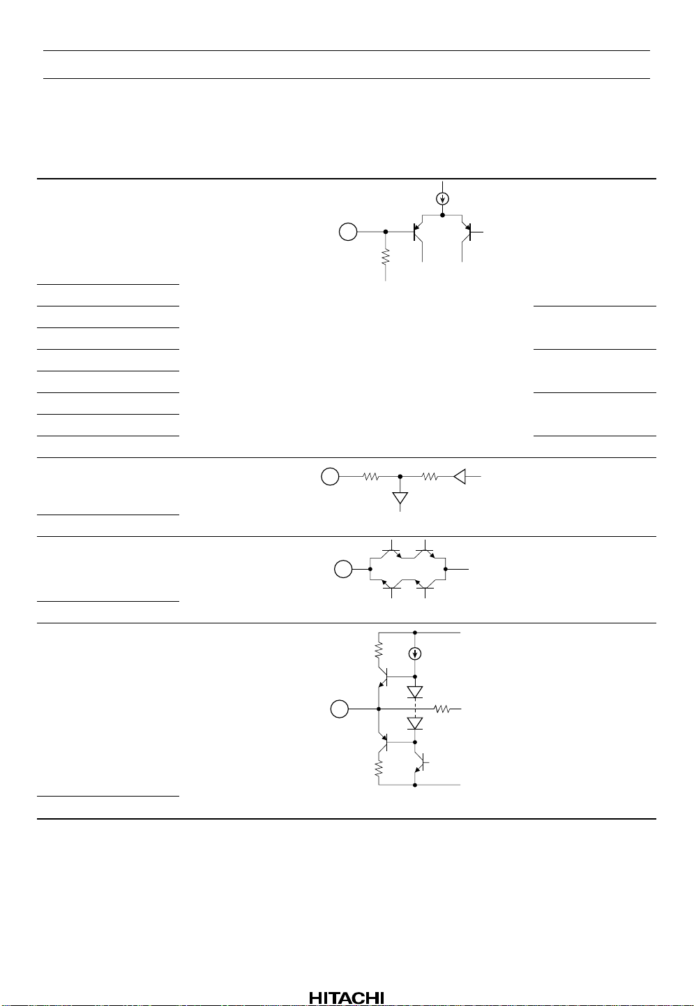
HA12206NT
Pin Description, Equivalent Circuit (VCC = 7.0V, VEE = –7.0V, Ta = 25°C, No signal,
The value in the table show typical value.)
Pin No. Pin Name Note Equivalent Circuit Pin Description
2 PB-Ain (R) V=0
V
100k
29 PB-Ain (L)
4 PB-Bin (R) B Deck PB input
27 PB-Bin (L)
5 REC-in (R) REC input
26 REC-in (L)
9 EQ-in (R) Equalizer input
22 EQ-in (L)
12 MIMS MS Gain control
3 AB out (R) V = 0
14.9k 10.6k
V
A Deck PB input
Time constant for
NAB standard
28 AB out (L)
6 ATT (R) V = 0
25 ATT (L)
7RPOUT (R)
24 RPOUT (L)
Variable
V
V
CC
V
EE
impedance for
attenuation
REC or PB output
Rev.3, Jun. 1999, page 2 of 32
Page 3
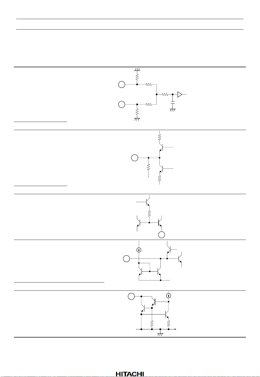
HA12206NT
Pin Description, Equivalent Circuit (VCC = 7.0V, VEE = –7.0V, Ta = 25°C, No signal,
The value in the table show typical value.) (cont)
Pin No. Pin Name Note Equivalent Circuit Pin Description
8 ADD in (R)
23
100k
100k
100k
Adder input
23 ADD in (L)
10 EQOUT (R) V = 0V
21 EQOUT (L)
11 IREF V = 1.2V
13 DET MS V = VCC – 4.2V
8
100k
100k
Equalizer output
100k
V
Equalizer
reference current
input
V
V
Time constant for
rectifier
15 DET ALC V = 2.3V
16 MS MS output
Rev.3, Jun. 1999, page 3 of 32
Page 4
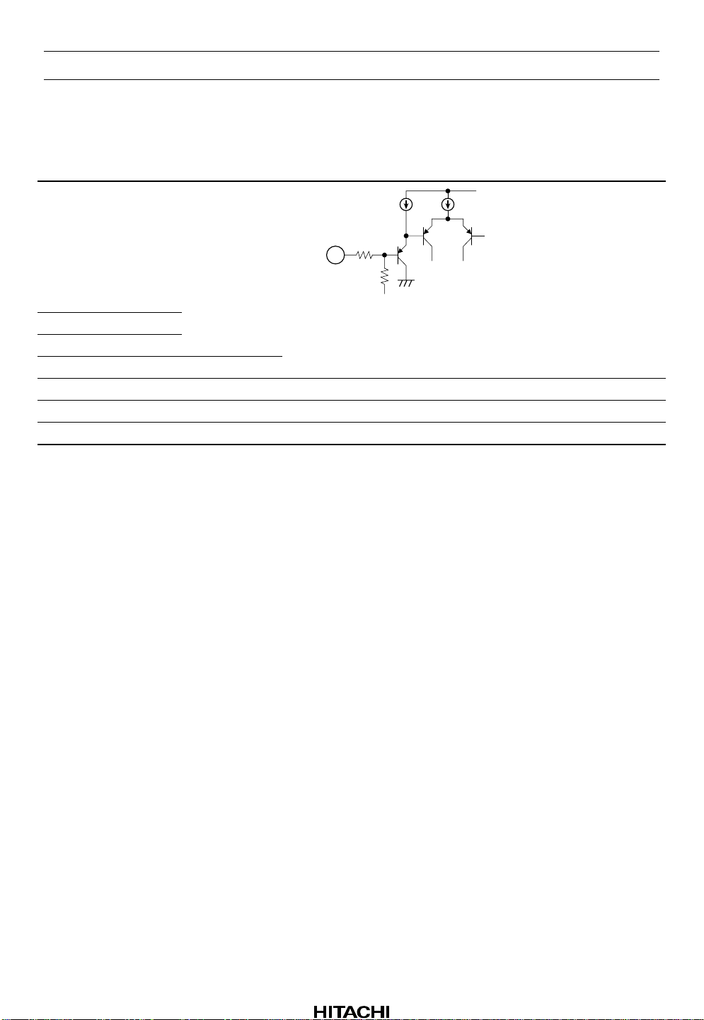
HA12206NT
Pin Description, Equivalent Circuit (VCC = 7.0V, VEE = –7.0V, Ta = 25°C, No signal,
The value in the table show typical value.) (cont)
Pin No. Pin Name Note Equivalent Circuit Pin Description
17 Acr V = 0V
22k
100k
V
V
CC
18 Bcr
19 REC MUTE
20 REC / A / B V = 2.5V
1V
14 V
EE
CC
30 GND GND pin
Mode control
VEE pin
VCC pin
Rev.3, Jun. 1999, page 4 of 32
Page 5
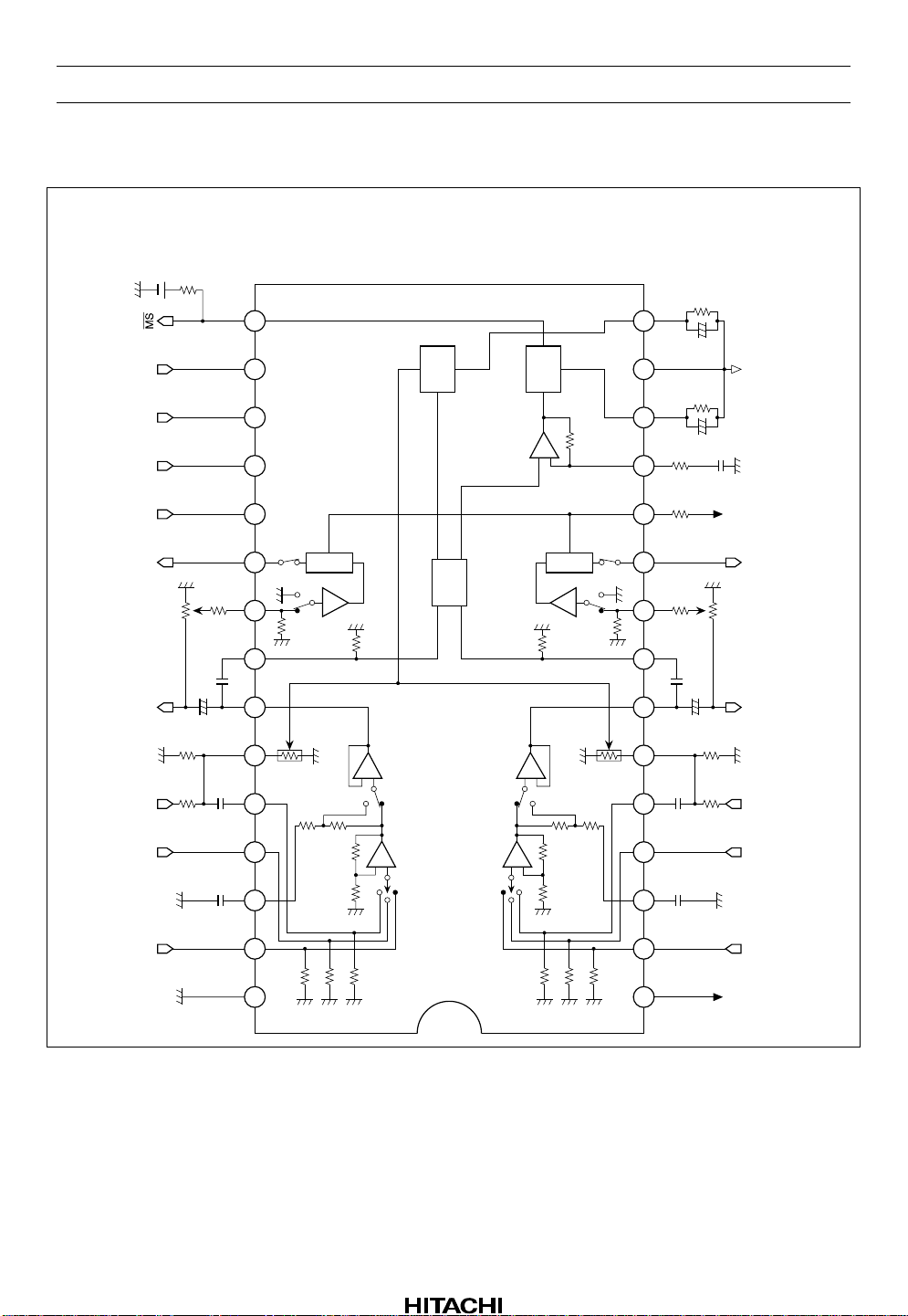
Block Diagram
HA12206NT
C : F
Acr
Bcr
RECMUTE
or
(L)
RECOUT
5V
C/N
(SW2)
C/N
(SW2)
(SW3)
ON/OFF
(SW1)
REC/A/B
(L)
EQOUT
(L)
PBOUT
(L)
REC in
(L)
PB Bin
(L)
PB Ain
R3L
GND
R8
R2L
R1L
3.9k
C4L
2.2k
15k
0.1µ
+
C3L
C2L
C1L
0.1µ
4700p
16
BCR ACR MS
RECMUTE
100k
25 24 23 22 21 20 19 18 17
−30dBs−30dBs −30dBs
AINL ABOUTL BINL RECINL ATTL RPOUTL ADDINL EQINL EQOL RECAB
30 29 28 27 26
SW4L
Mute
SW3L
14.9k
100k
REC⋅EQ
20dB
10.6k
22.7k
1k
100k
67k
−2.5dBs
(580mV)
−
+
C
−
+
REC
B
100k
N
27.5dB
SW2L
SW1L
A
ALC
DET
ADDER
SW2R
27.5dB
+
SW1R
A
−2.5dBs
+
N
−
B
MS
+
67k
(580mV)
−
C
REC
100k
DET
−
20dB
(1.64Vpp)
10.6k
22.7k
1k
100k
100k
REC⋅EQ
SW3R
14.9k
100k
Unit R : Ω
R7
1M
15
C7
10µ
CC
+7V
V
R6
330k
+ +
C6
0.33µ
C5
R5
68k
MIMS DETMS DETALC
IREF
(436mV)(38.8mV)
SW4R
Mute
100k
ADDINR EQINR EQOR
RPOUTR
67891011121314
−30dBs −26dBs −5dBs
−30dBs
BINR RECINR ATTR
ABOUTR
AINR
−30dBs
(24.5mV)
12345
R4
C2R
C1R
0.1µ
C4R
+
C3R
0.1µ
4700p
R2R
R1R
2.2k
15k
2200p
EE
V
R3R
EE
V
(R)
EQOUT
(R)
RECOUT
(R)
REC in
(R)
PB Bin
(R)
PB Ain
−7V
or
(R)
PBOUT
(180mV)
−12.7dBs
Rev.3, Jun. 1999, page 5 of 32
Page 6

HA12206NT
Truth Table
Parallel Data Format
NAB SW Position (SW 2)
REC / AAAA / BBBB (Pin 20)
Acr (Pin 17) Bcr (Pin 18) L M H REC-EQ Mode
L L TYPE
L H TYPE II TYPE I TYPE I TYPE II
H L TYPE
H H TYPE
Line Amp (SW 1) B A REC
ALC OFF OFF *1
REC-EQ Behind (SW 4) OFF ON ON
Note: 1. Follow the position of REC-MUTE pin.
I
I
II
TYPE
TYPE
TYPE
I
II
II
TYPE
TYPE
TYPE
I
I
I
TYPE
TYPE
TYPE
I
I
II
REC-MUTE (Pin 19) REC-EQ Before (SW 3) ALC
LActiveON
HMUTEOFF
Control Pin Position Under the Open Case
Acr (Pin 17) L
Bcr (Pin 18) L
REC-MUTE (Pin 19) L
REC / A / B (Pin 20) M
Rev.3, Jun. 1999, page 6 of 32
Page 7
Test Conditions
(0.5dB)
(0.5dB)
V(DC SOURCE 1)
IL
V
0.3dB
V(DC SOURCE 1)
IM
V
IM
V
60dB
(dB)
V(AC VM2)
(0.5dB)
V(DC SOURCE 1)
IH
(RECAB)
V
IH
V
(REC-MUTE)
V(DC SOURCE 1)
IH
V
(Acr, Bcr)
HA12206NT
=20 log {V(AC VM2 / Vi)}
V
=I (DC SOURCE 3)
Q
V(AC VM2)
I
Measure
—
AC VM2
AC VM2
AC VM2
—
PBOUT
PBOUT
EQOUT
—
Ain
Bin
EQin
—
10kHz, –30dBs
10kHz, –30dBs
1kHz, –26dBs
123
Q
I
Acr
4
Bcr
REC-MUTE
(dB)
(dB)
V(AC VM2)
AC VM2
AC VM2
RPOUT
RPOUT
Bin
Ain
1kHz, –30dBs
1kHz, –30dBs
5
5
RECAB
RECAB
(dB)
V(AC VM2)
AC VM2
AC VM2
AC VM2
AC VM2
EQOUT
RPOUT
RPOUT
RPOUT
Ain
Bin
EQin
RECin
10kHz, –30dBs
10kHz, –30dBs
1kHz, –26dBs
1kHz, –30dBs
234
Acr
Bcr
REC-MUTE
5
RECAB
=20 log {V(AC VM2) / V(AC VM1)}
=20 log {V(AC VM2) / V(AC VM1)}
V
G
AC VM1
AC VM2
RPOUT
Ain
1kHz, –30dBs
6
(1)
V
G
=20 log {V(AC VM2) / V(AC VM1)}
V
V
G
G
Vi=V(AC VM2) at SW5, SW6=REC
AC VM1
AC VM2
AC VM1
AC VM2
AC VM2 G
RPOUT
RPOUT
RPOUT
Bin
Bin
1kHz, –30dBs
10kHz, –30dBs
1kHz, –30dBs
7
8
9 RECin
(2)
(3)
V
G
(4)
V
G
Vo=V(AC VM2) at T.H.D=1% Vomax=20 log (Vo / 580mV)
AC VM2
RPOUT
Ain
1kHz
6
V
Vomax
400 to 30kHz BPF
400 to 30kHz BPF
Distortion
Distortion
Analyzer
RPOUT
RPOUT5-2 THD(2)
RECin
1kHz, –30dBs
1kHz, –0.7dBs
9
6
Analyzer
Test No. Set No.Symbol SG. Input Output Other12-1
(VIL)
2-2
(VIM)
2-3
(VIH)
3-1
3-2
3-3
4
5-1 THD(1) Ain
3-4 G
Rev.3, Jun. 1999, page 7 of 32
Page 8

HA12206NT
Test Conditions (cont)
=20 log {V(AC VM2) / 580mV} at DC VM=
S/N=20 log {580mV / V(Noise)} CCIR / ARM
CT=20 log {580mV / V(AC VM2)}
——AC VM2
RPOUT
RPOUT
RPOUT
——Ain
Input Output Measure
——1kHz, –18dBs*
69101112
S/N (1) S/N=20 log {580mV / V(Noise)} CCIR / ARM
S/N (2)
CT R/L
Test No. Set No.Symbol SG. Other
6-1
6-278910
ON
CT=20 log {580mV / V(AC VM2)}
ALC=20 log {V(AC VM2) / 580mV}
V
AC VM2
AC VM2
AC VM2
RPOUT
RPOUT
RPOUT
Ain/Bin
RECin
Ain
1kHz, –18dBs*
1kHz, –0.7dBs
5kHz
6
ONVOL
CT A/B
ALC
V
REC=20 log {V(AC VM2) / V(AC VM1)}
REC=20 log {V(AC VM2) / V(AC VM1)}
REC=20 log {V(AC VM2) / V(AC VM1)}
V
V
V
G
G
G
DC VM
DC VM
AC VM2
AC VM2
AC VM2
EQout
RPOUT
EQout
EQout
Ain
EQin
EQin
EQin
1kHz, –30dBs
1kHz, –46dBs
8kHz, –46dBs
12kHz, –46dBs
6131313131313
REC N1
REC N2
REC N3
V
V
V
G
G
G
11
12-1
12-2
12-3
REC=20 log {V(AC VM2) / V(AC VM1)}
REC=20 log {V(AC VM2) / V(AC VM1)}
REC=20 log {V(AC VM2) / V(AC VM1)}
V
V
V
G
G
G
AC VM2
AC VM2
EQout
EQout
EQin
EQin
1kHz, –46dBs
8kHz, –46dBs
at T.H.D=1%
R-MUTE ATT=20 log {436mV / V(AC VM2)}
400 to 30kHz BPF
S/N=20 log {436mV / V(AC VM2)}
AC VM2
AC VM2
EQout
EQout
EQin
1kHz, –14dBs*
12kHz, –46dBs
AC VM2
EQout
EQin
1kHz
Noise
Distortion
Analyzer
EQout
EQout17 S/N REC 13
—
1kHz, –26dBs
—
Meter
13
REC C1
REC C2
REC C3
V
V
V
G
G
G
Vomax REC
13-1
13-2
13-3
15
16 THD REC 13 EQin
14 R-MUTE ATT 14 EQin
Note: or large level without dipping
Rev.3, Jun. 1999, page 8 of 32
Page 9

Test Conditions (cont)
SW Position (Pre-Set for Each TEST)
4
–7V
–7V
–7V
–7V
–7V
–7V
–7V
–7V
–7V
–7V
–7V
3
–7V
–7V
–7V
–7V
–7V
–7V
–7V
–7V
–7V
–7V
–7V
–7V
–7V
–7V
–7V
–7V
–7V
–6V
–6V
HA12206NT
–6V
–6V
25V5V5V5V5V5V5V5V5V5V5V5V
CC
DC-SOURCE(V)
1
2.5V
0 to V
0 to VCC0 to VCC0 to VCC2.5V*1*1*12.5V
10MOFFLHMMLLHM
9LLLMLHHHHHHL
8LLMLLLLHLLLL
LMLLLLLLLLL
*1RPRPEQRPRPRPRPRPRPRP
67
5*1RPRPEQRPRPRPRPRPRPRPRP
5V5V5V
5V
2.5V*12.5V
2.5V
L⇔M
H
M
M
HLH
L
LLL
L
L
LLL
L
RP
EQEQRP
EQ
EQEQRP
EQ
2.5V
M
2.5V
M
*1*2*2*2*2*2*2*2*2
*1ABEQBABBRECAA⇔B
34
2*1ABEQBABB
SW-Position
1
OFF*2*2*2*2*2*2*2*2
Set No.1234567891011121513
L⇔R*2*2
RECAA⇔B
R⇔L*2*2
REC
REC
*2
EQ
EQ
*2
*2*2*2
EQ
EQ
*2*2*2
14
EQ
A
A
EQ
16
2. Measured channel Lch or Rch
Note: 1. Either will do
Rev.3, Jun. 1999, page 9 of 32
Page 10
HA12206NT
Functional Description
Power Supply Range
Table 1 Supply Voltage
Power Supply Range
Item V
CC
Single Supply 6.0V to 7.5V –7.5V to –6.0V Inside 1.0V
Note: HA12206NT is designed to operate on split supply.
As VEE pin is joined the substrate of chip, there is the possibility of latch-up in such case that the other pin is
supplied a voltage and V
pin is open.
EE
V
EE
| VCC | – | VEE |
Therefore please use as V
pin become the lowest voltage of low impedance all the time. When power
EE
supply is thrown into this IC, that caution is necessary especially.
Operating Mode Control
HA12206NT provides fully electronic switching circuits. And each operating mode control is controlled by
parallel data (DC voltage).
Table 2 shows the control voltage of each control input pin.
Table 2 Control Voltage
Pin No. Lo Mid Hi Unit Test Condition
17, 18, 19 0.0 to 1.0 — 4.0 to V
20 0.0 to 1.0 2.0 to 3.0 4.0 to V
V
CC
V
CC
Note: 1. Each pin is pulled down with 100kΩ internal resistor. 17 to 19 pins are low-level, 20 pin is mid-
level, when each pin is open.
2. Over shoot level and under shoot level of input signal must be the standardi ze d.
(High: Less than V
, Low: More than –0.2V)
CC
Input Pin Measure
Rev.3, Jun. 1999, page 10 of 32
Page 11

HA12206NT
PB Equalizer
By switching logical input level of pin17 (for Ain) or pin18 (for Bin), you can equalize corresponding to
tape position at play back mode.
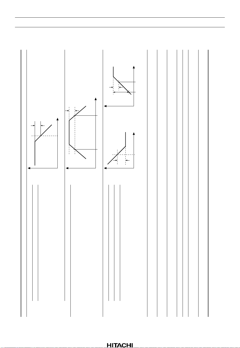
Frequency characteristics of high position (TYPE II) depends on capacitor C1 on the block diagram figure.
Figure 1 is shown by a motive of the NAB standard.
G
V
τ1 = C1
• (10.6k+14.9k)
• 14.9k
τ2 = C1
f
τ1 τ2
Figure 1 Frequency Characteristics of PB Equalizer
Music Sensor
C4 L
C4 R
0.33µ
to ALC
100k
23
8
100k
LR addend stage Detection stage
to ALC
100k
100k
100k
43p
Amplification stage
+
–
100k
12
R5C568k
2200p
V
CC
13
MS
DET
330k
Output stage
16
D V
CC
(5V)
22k
Figure 2 Music Sensor Block Diagram
Rev.3, Jun. 1999, page 11 of 32
Page 12

HA12206NT
The Sensitivity of Music Sensor
Frequency characteristics of MS amplification stage is shown by figure 3.
G
V
1
• C5 • (R5 + 100k)
1
• C5 • R5
f1 f2 f3
f1 = [Hz]
2π
f2 = [Hz]
2π
f3 = 25k [Hz]
f
Figure 3 Frequency Characteristic of MS AMP
Occasion of the external component of figure 2, f1 is 430Hz and f2 is 1.1kHz.
As the MS sensitivity is prescribed at 5kHz, this stage’s gain is 7.9dB. But in only one-sided channel input
case, this gain is considered as –6dB down, because the other channel input pin is imaginary earth. That is,
the gain from RPOUT to MSDET is 1.86dB.
As the detection sensitivity at MSDET is fixed 130mVrms, the sensitivity at RPOUT (8 pin or 23 pin) is
calculated by the following formula.
130mV
10 ^
1.86
20
= 105mV
Because of RPOUT=580mVrms=0dB, therefore, the MS sensitivity becomes –14.8dB.
That is the detection level.
Time Constant of Detection
Figure 4 (1) generally shows that detection time is in proportion to value of capacitor C16. But, with
Attack*
1
and Recovery*2 the detection time differs exceptionally.
Note: 1 . Attack : Non-music → Music
2. Recovery : Music → Non-music
Recovery
Attack
Detection time
C6
Function Characteristics of MS (1) Function Characteristics of MS (2) Function Characteristics of MS (3)
Recovery Recovery
Attack Attack
Detection time
R6
Detection level
Detection time
Input level
Figure 4 Function Characteristic of MS
Like the figure 4 (2), Recovery time is variably possible by value of resistor R6. But Attack time gets about
fixed value. Attack time has dependence by input level. When a large signal is inputted, Attack time is
short tendency.
Rev.3, Jun. 1999, page 12 of 32
Page 13

HA12206NT
Music Sensor Output (MSOUT)
Because MS out pin is connected to the collector of NPN type directly, it is requested to use pull up resistor
(RL=10k to 22kΩ)
Output level is “High” sensing no signal. And output level is “Low” sensing signal.
Please take notice of MS Low level voltage (GND+0.9V).
The connected supply voltage must be less than V
Automatic Level Control (ALC)
ALC is the input decay rate variable system.
It has internal variable resistors of pin6 (pin25) by RECOUT signal that is inputted to pin8 (pin23).
The operation is similitude to MS, detected by pin15.
The signal input pin is pin5 (pin26). Resistor R1, R2 and capacitor C2, external components, for the input
circuit are commended as figure 6. These are requested to use value of the block diagram figure for
performance maintenance of S/N, T.H.D. etc.
Figure 5 shows the relation with R1 front REC IN point and RPOUT.
ALC operation level is 775mVrms {standard level (580mVrms) +2.5dB}. And it is designed to operate
from 0dB to +15dB as 775mVrms=0dB.
Adopted maximum value circuit, ALC is operated by a large channel of a signal.
ALC on/off is linked with REC mu te. When REC mute is on, ALC is off.
voltage, with MSOUT pull up resistor.
CC
775mV
580mV
RPOUT
2.5dB
15dB
RECIN
Figure 5 ALC Operation Level
Input
RECIN
R1 24.5mV 27.5dB
C2
5
R2
ATT
6
ALC
RPOUT
580mV
7
8
ADDIN
DETALC
15
C4
Output
R7
+
C7
V
CC
Figure 6 ALC Block Diagram
REC-Equalizer
REC mute is located at input-part of REC-equalizer. Therefore it has realized low pop noise.
But because there is deference DC offset at the each mode of REC-equalizer, it is necessary for a coupling
capacitor between EQOUT pin and recording head.
Rev.3, Jun. 1999, page 13 of 32
Page 14

HA12206NT
Absolute Maximum Rating (Ta = 25°C)
Item Symbol Rating Unit Note
Max supply voltage V
Max supply voltage VEE max –8 V
Power dissipation Pd 500 mW Ta≤75°C
Operating temperature Topr –40 to +75 °C
Storage temperature Tstg –55 to +125 °C
Operating voltage Vopr VCC=–VEE=6 to 7.5 V
max +8 V
CC
Rev.3, Jun. 1999, page 14 of 32
Page 15

HA12206NT
Electrical Characteristics (Ta=25°C, VCC=±7.0V (VEE), 0dB=580mVrms=–2.52dBs
(Vout))
1
Note
2
2, 3
3
14
17 to 202017 to 20
Output
RL
L
Input
R COM
No signal
Vin
(dBs)———–30
—
fin
(Hz) Other
———1k1k
—
———
TYPE I
Acr Bcr
TYPE I
———
REC
Test Condition Application Terminal
IC Condition
REC/
———
MUTE
Active
A/BA———ABBRECAA
24
24
72477
7
7
29
27
27
244
0dB
0dB
0dB
–30
–30
10k1k1k1k1k
TYPE I
TYPE I
TYPE II
TYPE I
TYPE I
TYPE I
Mute
Mute
Mute
242424
7
29
29
26
522
30kHz
to
0dB
THD=1%
0dB, BW 400Hz
–30—–30
TYPE I
TYPE I
TYPE I
TYPE I
TYPE I
TYPE I
Mute
Mute
Mute
724
724
724
29
29
26
5
2
2
+12dB (ALC ON)
BW 400Hz to 30kHz
–0.7
TYPE I
TYPE I
Active
REC
Rg=2.2kΩ, CCIR/ARM
S=580mVrms
Rg=10kΩ, CCIR/ARM
S=580mVrms
—
—
—
—
TYPE I
TYPE I
TYPE I
TYPE I
Mute
Mute
A
REC
24
7
29
29 24 7–18
2
+12dB
+12dB
–18
1k
1k
TYPE I
TYPE I
TYPE I TYPE I
Mute
Mute
A/B
AChannel separation CT R/L 70 80 — dB 2
16
27
29
29
26
4
+12dB (ALC ON)
5k 7 24—
— 724—
1k 7 24–0.7
TYPE I TYPE I
TYPE I TYPE I
TYPE I TYPE I
Mute
Mute
Active
AAREC
mAVVVdBdBdBdBdB%%
22.0
16.0———27.5
10.0
Q
I
Item Symbol Min Typ Max Unit
Quiescent current
CC
1.0
3.0
V
29.0
29.0
27.5
–0.2
2.0
4.0
26.0
26.0
(1)
(2)
V
V
VILVIMVIHG
Logical threshold
G
Line amp. gain
24.9
29.0—0.3
22.9
27.5
20.9
26.0
(3)
(4)
V
G
G
V
13.0
0.05
12.0——
THD(1)
THD
Maximum output Vomax
dB
3.0
—
1.0
78
70
THD(2)
S/N(1)
Signal to noise ratio
dB
—
81
73
S/N(2)
dB
—
70
60
CT A/B
Crosstalk
ALC operation level ALC 0.0 2.5 5.5 dB 5
dB 2
–18.7 –14.7 –10.7
— 1.0 1.5 V 2
ON
OL
) = ±6.0V
EE
(V
CC
2. From REC in point
3. For inputting signal to one side channel
MS sensing level V
MS output low level V
Note: 1. V
Rev.3, Jun. 1999, page 15 of 32
Page 16

HA12206NT
Electrical Characteristics (Ta=25°C, VCC=±7.0V (VEE), 0dB=580mVrms=–2.52dBs
(Vout)) (cont)
Output
Input
EQin
fin
Note
RL
R L COM
9221021
9221021
(dBs)
–46
–46
(Hz) Other
8k
1k
TYPE I
TYPE I
TYPE I
TYPE I
Acr Bcr
9221021
9221021
9221021
–46
–46
–46
12k1k8k
TYPE I
TYPE IITYPE IITYPE
TYPE I
TYPE I
TYPE I
4
9221021
9221021
9221021
9221021
THD=1%
+12dB
–46
–14
—
–26
12k1k1k1k—
II
TYPE I
TYPE I
TYPE I
TYPE I
TYPE I
TYPE I
TYPE I
9221021
Rg=5.1kΩ, A-WTG
S=–5dBs
—
TYPE I
TYPE I
REC-
MUTE
Active
Active
Active
Test Condition Application Terminal
IC Condition
REC/
A/BAAAAAA
dBdBdBdBdBdBdB
21.7
27.1
34.4
20.2
25.1
31.4
18.7
23.1
28.4
REC-N1
REC-N2
REC-N3
V
V
V
G
G
G
Item Symbol Min Typ Max Unit
REC-EQ frequency
response
Normal speed
Normal tape
Active
Active
Active
Mute
Active
A
AAA
dBs%dB
25.6
32.5
39.4——
24.1
30.5
36.4807.0
22.6
28.5
33.2704.0—52
REC-C1
REC-C2
REC-C3
V
V
V
G
G
G
R-MUTE ATT
REC-MUTE
attenuation
REC-EQ frequency
response
Normal speed
Chrom tape
REC-EQ maximum output Vomax REC
Active
Active
0.7
—
0.35
60
THD REC
S/N REC
=±6.0V (V)
CC
REC-EQ S/N
REC-EQ THD
Note: 4. V
Rev.3, Jun. 1999, page 16 of 32
Page 17

Test Circuit
HA12206NT
Rev.3, Jun. 1999, page 17 of 32
Page 18
HA12206NT
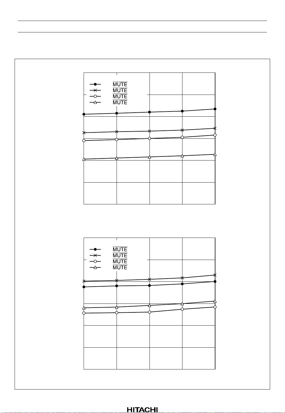
Characteristic Curves
18
17
16
(mA)
CC
15
14
Quiescent Current I
13
Quiescent Current vs. Supply Voltage (PB mode)
Ta=25˚C
Ain, , Nor
Bin, , Nor
Ain, , Cro
Bin, , Cro
12
5
Quiescent Current vs. Supply Voltage (REC mode)
18
Ta=25˚C
Ain, , Nor
17
16
(mA)
CC
15
14
Quiescent Current I
13
12
5
Bin, , Nor
Ain, , Cro
Bin, , Cro
678
Supply Voltage VCC (V)
678
Supply Voltage VCC (V)
9
9
Rev.3, Jun. 1999, page 18 of 32
Page 19

Quiescent Current vs. Supply Voltage (PB mode)
–12
Ta=25˚C
Ain, , Nor
–13
–14
(mA)
EE
–15
–16
Quiescent Current I
–17
–18
–5
Bin, , Nor
Ain, , Cro
Bin, , Cro
–6 –7 –8
Supply Voltage VEE (V)
HA12206NT
–9
Quiescent Current vs. Supply Voltage (REC mode)
–12
Ta=25˚C
Ain, , Nor
–13
–14
(mA)
EE
–15
–16
Quiescent Current I
–17
–18
–5
Bin, , Nor
Ain, , Cro
Bin, , Cro
–6 –7 –8
Supply Voltage VEE (V)
–9
Rev.3, Jun. 1999, page 19 of 32
Page 20

HA12206NT
30
28
26
24
VCC=7V
Ta=25˚C
RPOUT vs. Frequency (1) Ain mode
120µ
22
(dB)
20
V RPOUT
18
G
16
14
12
10
10
30
28
26
24
VCC=7V
Ta=25˚C
70µ
100 1k 10k 100k
Frequency (Hz)
RPOUT vs. Frequency (2) Rin mode
1M
22
(dB)
20
V RPOUT
18
G
16
14
12
10
10
Rev.3, Jun. 1999, page 20 of 32
100 1k 10k 100k
Frequency (Hz)
1M
Page 21

RPOUT Total Harmonic Distortion vs. Input Level
10
VCC=7V, f=1kHz,
Vout=580mVrms
Ta=25˚C
Ain (NORM)
Ain (CROM)
Bin (NORM)
1.0
0.1
Total Harmonic Distortion T.H.D. (%)
0.01
–20
–10 0 10
Input Level Vin (dB)
HA12206NT
20
RPOUT Total Harmonic Distortion vs. Output Level
10
VCC=7V, f=1kHz,
Vout=580mVrms
Ta=25˚C
Rin (RM-ON)
Rin (RM-OFF)
1.0
0.1
Total Harmonic Distortion T.H.D. (%)
0.01
–20
–10 0 10
Output Level Vout (dB)
20
Rev.3, Jun. 1999, page 21 of 32
Page 22

HA12206NT
RPOUT Maximum Output Level vs. Supply Voltage
20
15
Ta=25˚C, f=1kHz,
RPOUT=580mVrms=0dB
10
5
Maximum Output Level Vomax (dB)
0
4
5768
Supply Voltage V
Ain
Bin
Rin RM-ON (ALC OFF)
Rin RM-OFF (ALC ON)
(V)
CC
9
RPOUT Signal to Noise Ratio vs. Supply Voltage
85
80
75
70
Signal to Noise Ratio S/N (dB)
65
4
5768
Supply Voltage VCC (V)
Ta=25˚C, CCIR/ARM
RPOUT=580mVrms=0dB
Ain NORM
Ain CROM
Bin
Rin RM-ON
Rin RM-OFF
9
Rev.3, Jun. 1999, page 22 of 32
Page 23

0
VCC=7V, Ta=25˚C,
0dB=RPOUT=580mV,
–10
Vin=+10dB,
Normal, Ain mode
–20
–30
–40
–50
–60
–70
Line Amp. Crosstalk (dB)
–80
–90
HA12206NT
Line Amp. Crosstalk vs. Frequency
Bin mode
Rin mode
(REC)
–100
100
0
VCC=7V, Ta=25˚C,
0dB=RPOUT=580mV,
–10
Vin=+10dB,
Normal, Ain mode
–20
–30
–40
–50
–60
–70
–80
Line Amp. Channel Separation (dB)
–90
1k 10k 100k 1M
Line Amp. Channel Separation vs. Frequency
10M
Frequency (Hz)
L→R
R→L
–100
100
1k 10k 100k 1M
Frequency (Hz)
Rev.3, Jun. 1999, page 23 of 32
10M
Page 24

HA12206NT
50
40
(dB)
30
V EQOUT
G
EQOUT vs. Frequency
VCC=7V
Ta=25˚C
Chrom
20
10
10
Norm
100 1k 10k
Frequency (Hz)
REC-EQ Total Harmonic Distortion (Normal) vs. Output Level
=7V, Ta=25˚C,
V
CC
400 to 30kHz BPF
10.0
5kHz
1.0
1kHz
100k
Total Harmonic Distortion T.H.D. (%)
0.1
–10
Rev.3, Jun. 1999, page 24 of 32
–55010
Output Level Vout (dBs)
15
Page 25

REC-EQ Total Harmonic Distortion (Chrom) vs. Output Level
VCC=7V, Ta=25˚C,
400 to 30kHz BPF
10.0
1.0
5kHz
Total Harmonic Distortion T.H.D. (%)
HA12206NT
0.1
–10
REC-EQ Maximum Output Level vs. Supply Voltage
20
T.H.D≥1%
Ta=25˚C
15
10
5
Maximum Output Level Vomax (dBs)
–55010
Output Level Vout (dBs)
Norm
Crom
1kHz
0
4
5768
Supply Voltage VCC (V)
Rev.3, Jun. 1999, page 25 of 32
9
Page 26

HA12206NT
REC-EQ Signal to Noise Ratio vs. Supply Voltage
70
0dB=Vout=-5dBs,
A-WTG, Ta=25˚C
65
60
55
REC-EQ Signal to Noise Ratio S/N (dB)
50
4
5768
Supply Voltage VCC (V)
Normal
Chrom
9
REQ-EQ Channel Separation vs. Frequency
60
VCC=7V, Ta=25˚C,
Vin=+12dB, Normal mode
40
20
reference
0
–20
–40
–60
–80
REQ-EQ Channel Separation (dB)
–100
–120
–140
10
100 1k 10k
R→R
R→L
L→R
100k
Frequency (Hz)
Rev.3, Jun. 1999, page 26 of 32
Page 27

60
VCC=7V, Ta=25˚C,
Vin=+20dB, Normal mode
40
HA12206NT
REQ-EQ Mute Attenuation vs. Frequency
20
0
–20
–40
–60
–80
REQ-EQ Mute Attenuation (dB)
–100
–120
–140
10
30
20
100 1k 10k
ALC Operate Level vs Input Level
VCC=7V, Ta=25˚C,
Single or Both input
100Hz to 10kHz
reference
Frequency (Hz)
,
, MUTE
B, MUTE
100k
10
0
Output Level (dB) 0dB=580mVrms
–10
–20
–20
–10 10020
Input Level Vin (dB) Rin=180mVrms=0dB
30
Rev.3, Jun. 1999, page 27 of 32
Page 28

HA12206NT
ALC Total Harmonic Distortion vs. Input Level
VCC=7V, Ta=25˚C,
Single or Both input
1.0
0.5
10kHz
100Hz
0.1
0.05
Total Harmonic Distortion T.H.D. (%)
0.01
–20
10
VCC=7V, Vin=+12dB,
Vout=580mVrms=0dB
Ta=25˚C
Single input
Both input
5
Output Level (dB)
0
1kHz
–10 10020
Input Level Vin (dB) Rin=180mVrms=0dB
ALC Operate Level vs. Frequency
30
–5
10
Rev.3, Jun. 1999, page 28 of 32
50 100
500 1k 5k 10k 50k
Frequency (Hz)
100k
Page 29

0
V
=7V, Ta=25˚C,
CC
–2
MSOUT
–4
–6
–8
–10
–12
MS Sensing Level (dB)
–14
–16
–18
HA12206NT
MS Sensing Level vs Frequency
Lo→Hi
Hi→Lo
–20
100
100
50
=7V, Ta=25˚C, f=5kHz MSOUT
V
CC
Ain→RPOUT=580mVrms=0dB
0dB
500 1k
–5dB
20
10
5
–10dB
14V
CC
13MSDET
2
1
Singnal Sensing Time (ms)
0.5
0.2
5k 10k 50k
Frequency (Hz)
Singnal Sensing Time vs. Capacitor
330kΩ
PBOUT
MSOUT
100k
0.1
0.01
0.05 0.1
Capacitor (mF)
0.5 1.0
Rev.3, Jun. 1999, page 29 of 32
Page 30

HA12206NT
1000
500
200
100
50
20
10
No Signal Sensing Time (ms)
5
No Signal Sensing Time vs. Resistor
=7V, Ta=25˚C, f=5kHz MSOUT
V
CC
Ain→RPOUT=580mVrms=0dB
0dB
–5dB
14
V
CC
0.33µF
13MSDET
+
PBOUT
(V)
MSOUT
V
2
1
10k
5
4
3
2
1
MSOUT
50k 100k 500k
Resistor (W)
MSOUT
vs. Resistor R
L
V
VCC=7V, Ta=25˚C, f=5kHz MSOUT
Ain→RPOUT=580mVrms=0dB
Vin=0dB
5V
R
L
16MSOUT
1M
0
100
500 1k
Rev.3, Jun. 1999, page 30 of 32
5k 10k 50k 100k 500k
Resistor R
(Ω)
L
1M
Page 31

Package Dimensions
30
HA12206NT
Unit: mm
27.10
28.10 Max
16
8.8
10.0 Max
115
1.5 Max
1.0
10.16
5.06 Max
1.78 ± 0.25
0.48 ± 0.10
2.54 Min
0.51 Min
0.25
1˚ – 13˚
Hitachi Code
JEDEC
EIAJ
Weight
(reference value)
+ 0.10
– 0.05
DP-30S
—
Conforms
1.98 g
Rev.3, Jun. 1999, page 31 of 32
Page 32

HA12206NT
Disclaimer
1. Hitachi neither warrants nor grants licenses of any rights of Hitachi’s or any third party’s patent,
copyright, trademark, or other intellectual property rights for information contained in this document.
Hitachi bears no responsibility for problems that may arise with third party’s rights, including
intellectual property rights, in connection with u se of the information contained in this document.
2. Products and product specifications may be subject to change without notice. Confirm that you have
received the latest product standards or specifications before final design, purchase or use.
3. Hitachi makes every attempt to ensure that its products are of high quality and reliability. However,
contact Hitachi’s sales office before using the product in an application that demands especially high
quality and reliability or where its failure or malfunction may directly threaten human life or cause risk
of bodily injury, such as aerospace, aeronautics, nuclear power, combustion control, transportation,
traffic, safety equipment or medical equipment for life support.
4. Design your application so that the product is used within the ranges guaranteed by Hitachi particularly
for maximum rating, operating supply voltage range, heat radiation characteristics, installation
conditions and other characteristics. Hitachi bears no responsibility for failure or damage when used
beyond the guaranteed ranges. Even within the guaranteed ranges, consider normally foreseeable
failure rates or failure modes in semiconductor devices and employ systemic measures such as failsafes, so that the equipment incorporating Hitachi product does not cause bodily injury, fire or other
consequential damage due to operation of the Hitachi product.
5. This product is not designed to be radiation resistant.
6. No one is permitted to reproduce or duplicate, in any form, the whole or part of this document without
written approval from Hitachi.
7. Contact Hitachi’s sales office for any questions regarding this document or Hitachi semiconductor
products.
Sales Offices
Hitachi, Ltd.
Semiconductor & Integrated Circuits.
Nippon Bldg., 2-6-2, Ohte-machi, Chiyoda-ku, Tokyo 100-0004, Japan
Tel: Tokyo (03) 3270-2111 Fax: (03) 3270-5109
URL NorthAmerica : http://semiconductor.hitachi.com/
For further information write to:
Hitachi Semiconductor
(America) Inc.
179 East Tasman Drive,
San Jose,CA 95134
Tel: <1> (408) 433-1990
Fax: <1>(408) 433-0223
Europe : http://www.hitachi-eu.com/hel/ecg
Asia : http://sicapac.hitachi-asia.com
Japan : http://www.hitachi.co.jp/Sicd/indx.htm
Hitachi Europe GmbH
Electronic Components Group
Dornacher Straße 3
D-85622 Feldkirchen, Munich
Germany
Tel: <49> (89) 9 9180-0
Fax: <49> (89) 9 29 30 00
Hitachi Europe Ltd.
Electronic Components Group.
Whitebrook Park
Lower Cookham Road
Maidenhead
Berkshire SL6 8YA, United Kingdom
Tel: <44> (1628) 585000
Fax: <44> (1628) 585160
Hitachi Asia Ltd.
Hitachi Tower
16 Collyer Quay #20-00,
Singapore 049318
Tel : <65>-538-6533/538-8577
Fax : <65>-538-6933/538-3877
URL : http://www.hitachi.com.sg
Hitachi Asia Ltd.
(Taipei Branch Office)
4/F, No. 167, Tun Hwa North Road,
Hung-Kuo Building,
Taipei (105), Taiwan
Tel : <886>-(2)-2718-3666
Fax : <886>-(2)-2718-8180
Telex : 23222 HAS-TP
URL : http://www.hitachi.com.tw
Copyright Hitachi, Ltd., 2000. All rights reserved. Printed in Japan.
Hitachi Asia (Hong Kong) Ltd.
Group III (Electronic Components)
7/F., North Tower,
World Finance Centre,
Harbour City, Canton Road
Tsim Sha Tsui, Kowloon,
Hong Kong
Tel : <852>-(2)-735-9218
Fax : <852>-(2)-730-0281
URL : http://www.hitachi.com.hk
Colophon 2.0
Rev.3, Jun. 1999, page 32 of 32
 Loading...