

Page 1

HA12187FP
Bus Interface Driver/Receiver IC
ADE-207-174A (Z)
2nd Edition
Jun. 1999
Description
The HA12187FP was developed to be used as a bus interface driver/receiver IC in automotive audio
equipment controllers. It implements a two-wire serial bus.
Functions
• Two-input OR circuit
• Input comparator circuit
• Current output driver circuit
• Receiver input comparator circuit
• Receiver output circuit
• Standby circuit
Features
• Supports two data inputs (Pins 1 and 3 are the input pins)
• Comparators with hysteresis characteristics were adopted for the inputs
• Current drive output drivers adopted (Output current: 3.8 mA typical)
• Comparators with hysteresis characteristics were adopted for the receivers
• Wide receiver common-mode input operating range (Common-mode input operating range: 0 to 5 V
typical)
• The driver output and the receiver input can withstand high voltages (Maximum rating: 18 V)
• Standby function (The IC enters standby mode when pin 8 goes low)
• Operating power-supply voltage range: 5 V ±0.5 V
Page 2
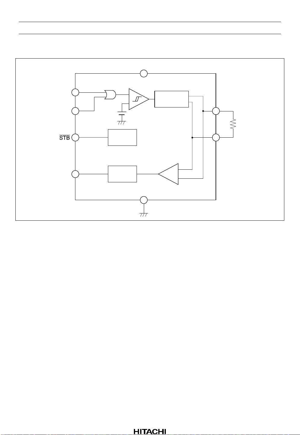
HA12187FP
Block Diagram
S1
V
CC
7
1
3S2
+
–
Driver output
(current)
BUS (+)
6
8
2R
BIAS
Receiver
output
COM
5
BUS (–)
–
+
4
Rev.2, Jun. 1999, page 2 of 23
Page 3
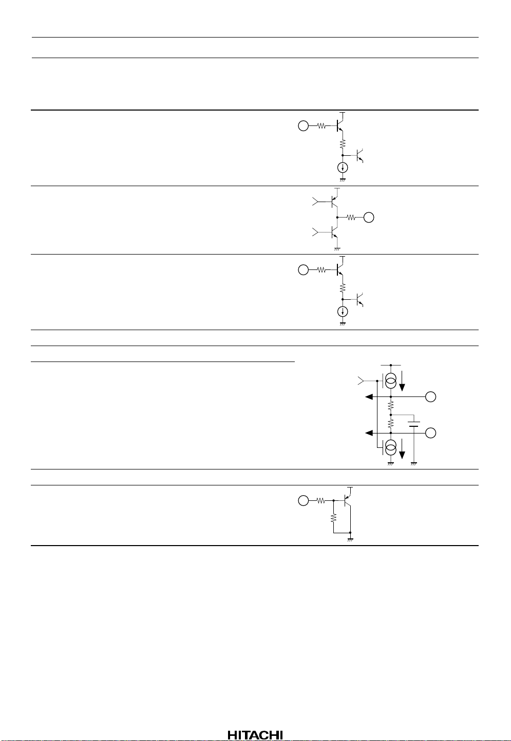
Pin Functions
Pin No. Symbol Function Equivalent Circuit
1 S1 Data input
1
20 k
HA12187FP
2 R out Receiver output
3 S2 Data input
4GNDGND
5 BUS (–) Bus output (–) Receiver input (–)
6 BUS (+) Bus output (+) Receiver input (+)
7VCCPower supply
8 STB Standby control input
SW
SW
3
Receiver input (+)
Receiver input (–)
8
20 k
100 k
100
20k
SW
2
I
6
V
REF
5
I
Rev.2, Jun. 1999, page 3 of 23
Page 4

HA12187FP
Absolute Maximum Ratings (Ta = 25°C)
Item Symbol Ratings Unit Notes
Power-supply voltage V
Allowable power dissipation Pd 400 mW Ta ≤ 85°C
Operating temperature Topr –40 to 85 °C
Storage temperature Tstg –55 to 125 °C
Input voltage Vin –1.0 to 6.7 V
Bus input voltage Bus 18 V
Note: Recommended operating power supply voltage range: 5 V ±0.5 V
CC
7V
Rev.2, Jun. 1999, page 4 of 23
Page 5

HA12187FP
Electrical Characteristics (VCC = 5.0 V, Ta = 25°C)
Test
Test
Item Symbol Min Typ Max Unit Test Conditions
S1 High-level input
voltage
V
IHS1
3.5 — — V V1 = 0 V → 5 V, V3 = 0 V
With the potential
difference between pin 5
and pin 6 120 mV or more
Low-level input
voltage
V
ILS1
— — 1.5 V V1 = 5 V → 0 V, V3 = 0 V
With the potential
difference between pin5
and pin 6 20 mV or less
High-level input
I
IHS1
— — 1 µA V1 = 5 V, V3 = 0 V 1
current
Low-level input
I
ILS1
— — 1 µA V1 = 0 V, V3 = 0 V 1
current
S2 High-level input
voltage
V
IHS2
3.5 — — V V3 = 0 V → 5 V, V1 = 0 V
With the potential
difference between pin 5
and pin 6 120 mV or more
Low-level input
voltage
V
ILS2
— — 1.5 V V3 = 5 V → 0 V, V1 = 0 V
With the potential
difference between 5 and
pin 6 20 mV or less
High-level input
I
IHS2
— — 1 µA V1 = 0 V, V3 = 5 V 3
current
Low-level input
I
ILS2
— — 1 µA V1 = 0 V, V3 = 0 V 3
current
Driver High-level
I
OH
3.0 3.8 4.8 mA IOH = | V
OHD+
– V
| / 62 Ω 5, 6 Figure 1
OHD–
output current
Low-level output
leakage current
Reference
I
OL
V
OP+
— — 1 µA Pin 5 voltage = V
IOL = | V
OP+
– V
OP–
OP–
| / RI
2.3 2.5 2.7 V V1 = 0 V, V3 = 0 V 6
operating
voltage (+)
Reference
V
OP–
2.3 2.5 2.7 V V1 = 0 V, V3 = 0 V 5
operating
voltage (–)
Current drain 1 ICCH 5.5 7.3 9.5 mA V1 = 5 V, V3 = 0 V 7 Figure 1
Current drain 2 ICCL 1.7 2.2 2.7 mA V1 = 0 V, V3 = 0 V 7 Figure 1
Pin
Circuit
1 Figure 1
1
3 Figure 1
3
5, 6
Rev.2, Jun. 1999, page 5 of 23
Page 6

HA12187FP
Electrical Characteristics (VCC = 5.0 V, Ta = 25°C) (cont)
Item Symbol Min Typ Max Unit Test Condition
Recei
ver
Power supply off output
leakage current
STB on voltage VSTBon — — 1.5 V V8 = 5 → 0 V, V1 = 5 V, V8
STB off voltage VSTBoff 3.5 — — V V8 = 0 → 5 V, V1 = 5 V, V8
Standby mode current
drain
Standby mode leakage
current
Delay time (L → H) DLY1 — 600 800 nS See the operating
Delay time (H → L) DLY2 — 450 800 nS See the operating
Note: 1. I1 is the measured current when V6 = (V
High-level input
voltage (1)
Low-level input
voltage (1)
Input hysteresis
voltage (1)
High-level
common-mode
input voltage
Low-level
common-mode
input voltage
Receiver input
resistance*
1
High-level
output voltage
Low-level output
voltage
) – 0.3 V.
(V
OP+
V
IH1
— 80 120 mV V6 = 0 → 5 V, pin 2 = 4 V
or more, V1 = 0V, V3 = 0V,
V5 = V
V
IL1
20 45 — mV V6 = 5 → 0 V, pin 2 = 1 V
OP–
, V
IH1
= V6 – V5
or less, V1 = 0 V, V3 = 0 V,
V
V
IHYS1
IHCOM
V5 = V
10 35 60 mV V
IHYS1
= V
4.5 — — V V5 = 0 → 5 V, pin 2 = 4 V
OP–,VIL1
IH1
= V6 – V5
– V
IL1
or more, V1 = 0 V, V3 = 0
V, V6 – V5 = 120 mV
V
ILCOM
5 ——V V5 = 0 → 5 V, pin 2 = 1 V
or less, V1 = 0 V, V3 = 0 V,
V6 – V5 = 20 mV
RI 25 35 45
V
V
I
OLEAK
OH
OL
4.5 — — V V1 = 5 V, V3 = 0 V 2 Figure 1
— — 1.0 V V1 = 0 V, V3 = 0 V 2 Figure 1
——1 µAVCC off, V8 = 0 V, V6 = 5 V,
kΩ
V1 = 0 V,
0.6V
=
RI
I1−I2
V1 = 0 V, V3 = 0 V, SW1
on
≤ 20 µA
CC
≥ 4.5 mA
CC
I
CCstb
when I
when I
— 10 20 µA V1 = 5 V, V3 = 0 V, V8 = 0V7 Figure 4
Istb-Leak — — 1 µA V1 = 5 V, V3 = 0 V, V8 = 0
V, V6 = 5 V, SW1 on
waveform figure
waveform figure
) + 0.3 V, and I2 is the measured current when V6 =
OP+
Test
Test
Pin
Circuit
2 Figure 2
2 Figure 2
5 Figure 2
5 Figure 2
5, 6 Figure 3
5, 6 Figure 4
7 Figure 4
7 Figure 4
5, 6 Figure 4
2 Figure 5
2 Figure 5
Rev.2, Jun. 1999, page 6 of 23
Page 7
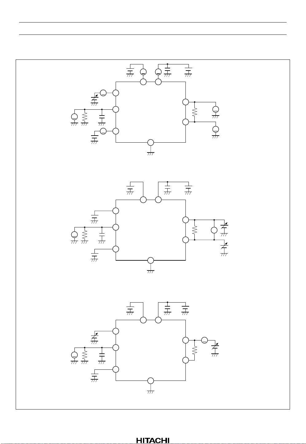
Test Circuits
HA12187FP
V8
5 V
A
A
1
2
20 p
3
V1
V
47 k
V3
0 V
A
8
HA12187FP
4
0.1 µ
A
7
V
CC
5 V
6
V
62 Ω
5
V
Test Circuit 1
V8
5 V
8
20 p
1
2
3
HA12187FP
4
V1
0 V
V
47 k
V3
0 V
0.1 µ
7
V
CC
5 V
6
62 Ω
5
V6
V
V5
Test Circuit 2
V8
5 V
8
20 p
1
2
3
HA12187FP
4
V1
V
47 k
V3
0 V
0.1 µ
7
V
CC
5 V
6
5
A
62 Ω
V6
Test Circuit 3
Rev.2, Jun. 1999, page 7 of 23
Page 8

HA12187FP
8V87
V
0.1 µ
A
5 V
CC
V1
5 V
47 k
V3
0 V
20 p + 14 pF
(probe
capacitance)
V3
0 V
20 p
47 k
1
2
3
HA12187FP
4
SW1
62 Ω
V6
5 V
A
V
6
5
Test Circuit 4
V8
5 V
1
2
3
A
8
HA12187FP
4
0.1 µ
A
7
V
CC
5 V
6
62 Ω
5
Oscilloscope
Rev.2, Jun. 1999, page 8 of 23
Test Circuit 5
Page 9

Operating Waveforms
Pin Waveform
5 V
S1 (or S2)
0 V
Bus (+)
Bus (–)
90%
HA12187FP
f = 50 kHz
Duty 50 %
10%
Bus (+) – Bus (–)
0 V
R (pin 2)
90%
10%
DLY1 DLY2
Rev.2, Jun. 1999, page 9 of 23
Page 10

HA12187FP
Main Characteristics
5
4.5
4
3.5
3
(V)
ILS1
2.5
, V
2
IHS1
V
1.5
1
0.5
0
3.5 4 4.5 5 5.5 6 6.5 7 7.5
VCC (V)
V
V
IHS1
ILS1
5
V
4.5
4
3.5
3
(V)
ILS2
2.5
, V
2
IHS2
V
1.5
1
0.5
0
3.5 4 4.5 5 5.5 6 6.5 7 7.5
V
IHS2
ILS2
VCC (V)
Rev.2, Jun. 1999, page 10 of 23
Page 11

10
I
9
8
7
6
(µA)
5
ILS1
, I
4
IHS1
I
3
2
1
0
3.5 4 4.5 5 5.5 6 6.5 7 7.5
IHS1
I
ILS1
VCC (V)
HA12187FP
10
I
9
8
7
6
IHS2
I
ILS2
(µA)
5
ILS2
, I
4
IHS2
I
3
2
1
0
3.5 4 4.5 5 5.5 6 6.5 7 7.5
VCC (V)
Rev.2, Jun. 1999, page 11 of 23
Page 12

HA12187FP
5
I
4.5
4
3.5
3
(µA)
OL
2.5
(mA), I
2
OH
I
1.5
1
0.5
0
3.5 4 4.5 5 5.5 6 6.5 7 7.5
OH
I
OL
VCC (V)
5
V
4.5
4
3.5
(V)
3
OP(–)
2.5
, V
2
OP(+)
V
1.5
1
0.5
0
3.5 4 4.5 5 5.5 6 6.5 7 7.5
V
OP(+)
OP(–)
VCC (V)
Rev.2, Jun. 1999, page 12 of 23
Page 13

10
9
8
7
6
L (mA)
5
CC
H, I
4
CC
I
3
2
1
0
3.5 4 4.5 5 5.5 6 6.5 7 7.5
ICCH
I
CC
L
VCC (V)
HA12187FP
100
90
80
70
(mV)
60
IHYS1
50
, V
IL1
40
, V
IH1
V
30
20
10
0
3.5 4 4.5 5 5.5 6 6.5 7 7.5
V
V
V
IH1
IL1
IHYS1
VCC (V)
Rev.2, Jun. 1999, page 13 of 23
Page 14

HA12187FP
10
9
8
(V)
7
ILCOM
V
6
IHCOM
V
5
V
IHCOM
V
ILCOM
4
3
3.5 4 4.5 5 5.5 6 6.5 7 7.5
V
(V)
CC
10
9
V
8
OH
V
OL
7
6
(V)
OL
5
V
OH
V
4
3
2
1
0
3.5 4 4.5 5 5.5 6 6.5 7 7.5
V
(V)
CC
Rev.2, Jun. 1999, page 14 of 23
Page 15

5
4.5
V
4
3.5
(V)
3
STBoff
2.5
, V
2
STBon
V
1.5
1
0.5
0
3.5 4 4.5 5 5.5 6 6.5 7 7.5
V
STBon
STBoff
VCC (V)
HA12187FP
1000
900
800
700
600
500
400
DLY1, DLY2 (V)
300
200
100
0
3.5 4 4.5 5 5.5 6 6.5 7 7.5
DLY1
DLY2
VCC (V)
Rev.2, Jun. 1999, page 15 of 23
Page 16

HA12187FP
5
4.5
4
3.5
3
(V)
ILS2
2.5
, V
2
IHS2
V
1.5
1
0.5
0
–50 –25 0 25 50 75 100
V
V
Ta (˚C)
IHS2
ILS2
5
4.5
4
3.5
3
(V)
ILS1
2.5
, V
2
IHS1
V
1.5
1
0.5
0
–50 –25 0 25 50 75 100
V
V
Ta (˚C)
IHS1
ILS1
Rev.2, Jun. 1999, page 16 of 23
Page 17

10
9
I
8
7
6
(µA)
5
ILS1
, I
4
IHS1
I
3
2
1
0
–50 –25 0 25 50 75 100
I
IHS1
ILS1
Ta (˚C)
HA12187FP
10
9
I
8
7
6
(µA)
5
ILS2
, I
4
IHS2
I
3
2
1
0
–50 –25 0 25 50 75 100
I
IHS2
ILS2
Ta (˚C)
Rev.2, Jun. 1999, page 17 of 23
Page 18

HA12187FP
5
4.5
4
3.5
I
3
(mA)
2.5
OL
, I
OH
2
I
1.5
1
0.5
0
–50 –25 0 25 50 75 100
OH
I
OL
Ta (˚C)
5
4.5
V
V
(µA)
4
3.5
3
OP(–)
2.5
, V
2
OP(+)
V
1.5
1
0.5
0
–50 –25 0 25 50 75 100
Ta (˚C)
OP(+)
OP(–)
Rev.2, Jun. 1999, page 18 of 23
Page 19

10
9
8
7
I
6
L (mA)
5
CC
H, I
4
CC
I
3
2
1
0
–50 –25 0 25 50 75 100
CC
I
CC
Ta (˚C)
HA12187FP
H
L
100
90
80
70
(mV)
60
IHYS1
50
, V
IL1
40
, V
IH1
V
30
20
10
0
–50 –25 0 25 50 75 100
V
V
V
Ta (˚C)
IH1
IL1
IHYS1
Rev.2, Jun. 1999, page 19 of 23
Page 20

HA12187FP
10
V
9
8
IHCOM
V
ILCOM
(V)
7
ILCOM
, V
6
IHCOM
V
5
4
3
–50 –25 0 25 50 75 100
Ta (˚C)
10
9
8
7
6
(V)
OL
5
, V
OH
4
V
3
2
1
0
–50 –25 0 25 50 75 100
V
V
Ta (˚C)
OH
OL
Rev.2, Jun. 1999, page 20 of 23
Page 21

5
4.5
4
3.5
(V)
3
STBoff
2.5
, V
2
STBon
V
1.5
1
0.5
0
–50 –25 0 25 50 75 100
V
V
Ta (˚C)
HA12187FP
STBon
STBoff
1000
900
800
700
600
500
400
DLY1
DLY2
DLY1, DLY2 (ns)
300
200
100
0
–50 –25 0 25 50 75 100
Ta (˚C)
Rev.2, Jun. 1999, page 21 of 23
Page 22

HA12187FP
Package Dimensions
1.27
4.85
5.25 Max
8
1
0.75 Max
Unit: mm
5
4.4
4
+ 0.25
6.50
– 0.15
2.03 Max
*0.22 ± 0.05
1.05
0.20 ± 0.04
0˚ – 8˚
+ 0.25
0.60
– 0.18
*0.42 ± 0.08
0.40 ± 0.06
*Dimension including the plating thickness
Base material dimension
0.10 ± 0.10
0.15
M
0.12
Hitachi Code
JEDEC
EIAJ
Weight
(reference value)
FP-8D
—
Conforms
0.10 g
Rev.2, Jun. 1999, page 22 of 23
Page 23

HA12187FP
Disclaimer
1. Hitachi neither warrants nor grants licenses of any rights of Hitachi’s or any third party’s patent,
copyright, trademark, or other intellectual property rights for information contained in this document.
Hitachi bears no responsibility for problems that may arise with third party’s rights, including
intellectual property rights, in connection with u se of the information contained in this document.
2. Products and product specifications may be subject to change without notice. Confirm that you have
received the latest product standards or specifications before final design, purchase or use.
3. Hitachi makes every attempt to ensure that its products are of high quality and reliability. However,
contact Hitachi’s sales office before using the product in an application that demands especially high
quality and reliability or where its failure or malfunction may directly threaten human life or cause risk
of bodily injury, such as aerospace, aeronautics, nuclear power, combustion control, transportation,
traffic, safety equipment or medical equipment for life support.
4. Design your application so that the product is used within the ranges guaranteed by Hitachi particularly
for maximum rating, operating supply voltage range, heat radiation characteristics, installation
conditions and other characteristics. Hitachi bears no responsibility for failure or damage when used
beyond the guaranteed ranges. Even within the guaranteed ranges, consider normally foreseeable
failure rates or failure modes in semiconductor devices and employ systemic measures such as failsafes, so that the equipment incorporating Hitachi product does not cause bodily injury, fire or other
consequential damage due to operation of the Hitachi product.
5. This product is not designed to be radiation resistant.
6. No one is permitted to reproduce or duplicate, in any form, the whole or part of this document without
written approval from Hitachi.
7. Contact Hitachi’s sales office for any questions regarding this document or Hitachi semiconductor
products.
Sales Offices
Hitachi, Ltd.
Semiconductor & Integrated Circuits.
Nippon Bldg., 2-6-2, Ohte-machi, Chiyoda-ku, Tokyo 100-0004, Japan
Tel: Tokyo (03) 3270-2111 Fax: (03) 3270-5109
URL NorthAmerica : http://semiconductor.hitachi.com/
For further information write to:
Hitachi Semiconductor
(America) Inc.
179 East Tasman Drive,
San Jose,CA 95134
Tel: <1> (408) 433-1990
Fax: <1>(408) 433-0223
Europe : http://www.hitachi-eu.com/hel/ecg
Asia : http://sicapac.hitachi-asia.com
Japan : http://www.hitachi.co.jp/Sicd/indx.htm
Hitachi Europe GmbH
Electronic Components Group
Dornacher Straße 3
D-85622 Feldkirchen, Munich
Germany
Tel: <49> (89) 9 9180-0
Fax: <49> (89) 9 29 30 00
Hitachi Europe Ltd.
Electronic Components Group.
Whitebrook Park
Lower Cookham Road
Maidenhead
Berkshire SL6 8YA, United Kingdom
Tel: <44> (1628) 585000
Fax: <44> (1628) 585160
Hitachi Asia Ltd.
Hitachi Tower
16 Collyer Quay #20-00,
Singapore 049318
Tel : <65>-538-6533/538-8577
Fax : <65>-538-6933/538-3877
URL : http://www.hitachi.com.sg
Hitachi Asia Ltd.
(Taipei Branch Office)
4/F, No. 167, Tun Hwa North Road,
Hung-Kuo Building,
Taipei (105), Taiwan
Tel : <886>-(2)-2718-3666
Fax : <886>-(2)-2718-8180
Telex : 23222 HAS-TP
URL : http://www.hitachi.com.tw
Copyright Hitachi, Ltd., 2000. All rights reserved. Printed in Japan.
Hitachi Asia (Hong Kong) Ltd.
Group III (Electronic Components)
7/F., North Tower,
World Finance Centre,
Harbour City, Canton Road
Tsim Sha Tsui, Kowloon,
Hong Kong
Tel : <852>-(2)-735-9218
Fax : <852>-(2)-730-0281
URL : http://www.hitachi.com.hk
Colophon 2.0
Rev.2, Jun. 1999, page 23 of 23
 Loading...