

Page 1

HA12173 Series
Audio Signal Processor for Car Deck and Cassette Deck
(Dolby B/C-type NR with PB Amp)
ADE-204-016
1st Edition
Nov. 1992
Description
HA12173 series are silicon monolithic bipolar IC providing Dolby noise reduction system*, music sensor
and PB equalizer system in one chip.
Functions
• PB equalizer × 2 channel
• Dolby B/C-NR × 2 channel
• Music sensor × 1 channel
Features
• Different type of PB equalizer characteristics selection (normal/chrome or metal) is available with fully
electronic control switching built-in.
• 2 type of input selection (RADIO/TAPE) is available.
• Changeable to Forward, Reverse-mode for PB head with fully electronic control switching built-in.
• Available to change music sensing level by external resistor.
• Music sensing level selection is available with fully electronic control switching built-in.
• Available to change frequency response of music sensor.
• NR-ON/OFF and REC/PB fully electronic control switching built-in.
• 4 type of PB-out level.
• Available to allow common PCB designs with HA12163 series.
* Dolby is a trademark of Dolby Laboratories Licensing Corporation.
A license from Dolby Laboratories Licensing Co r por ation is required for the use of this IC.
Page 2
HA12173 Series
Ordering Information
Operating voltage range*
Products PB-OUT level REC-OUT level Dolby-level Min Max
HA12173 300 mVrms 300 mVrms 300 mVrms 7.0V 16V
HA12174 450 mVrms 300 mVrms 300 mVrms 8.0V 16V
HA12175 580 mVrms 300 mVrms 300 mVrms 9.5V 16V
HA12177 775 mVrms 300 mVrms 300 mVrms 12.0V 16V
Note: 1. The minimum operating voltage of HA12173 series are defferent from the HA12163 series
(Dolby B - type).
1
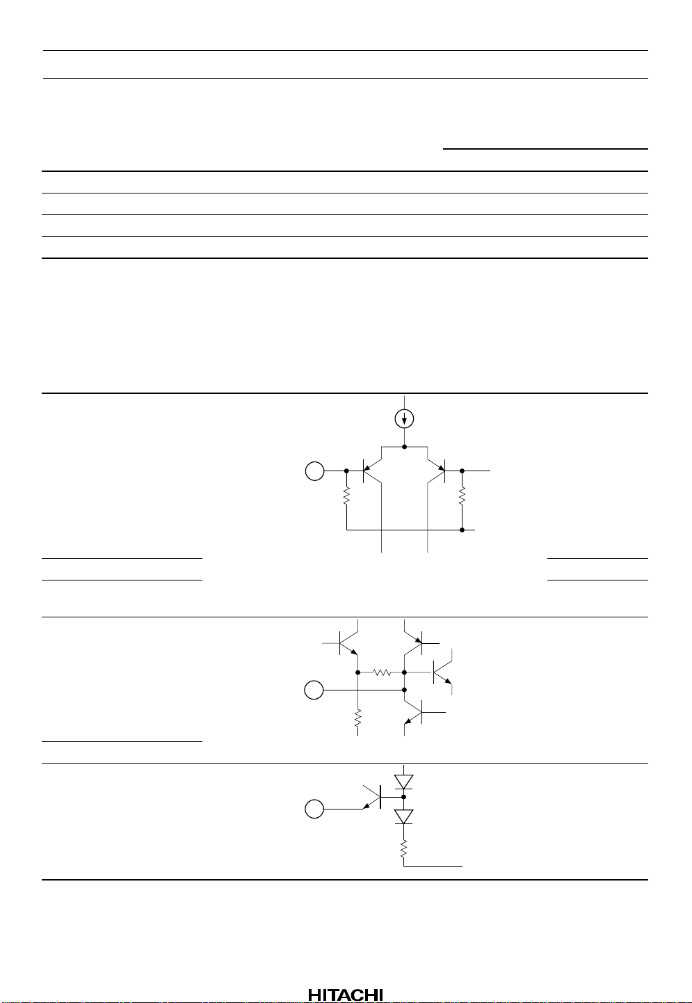
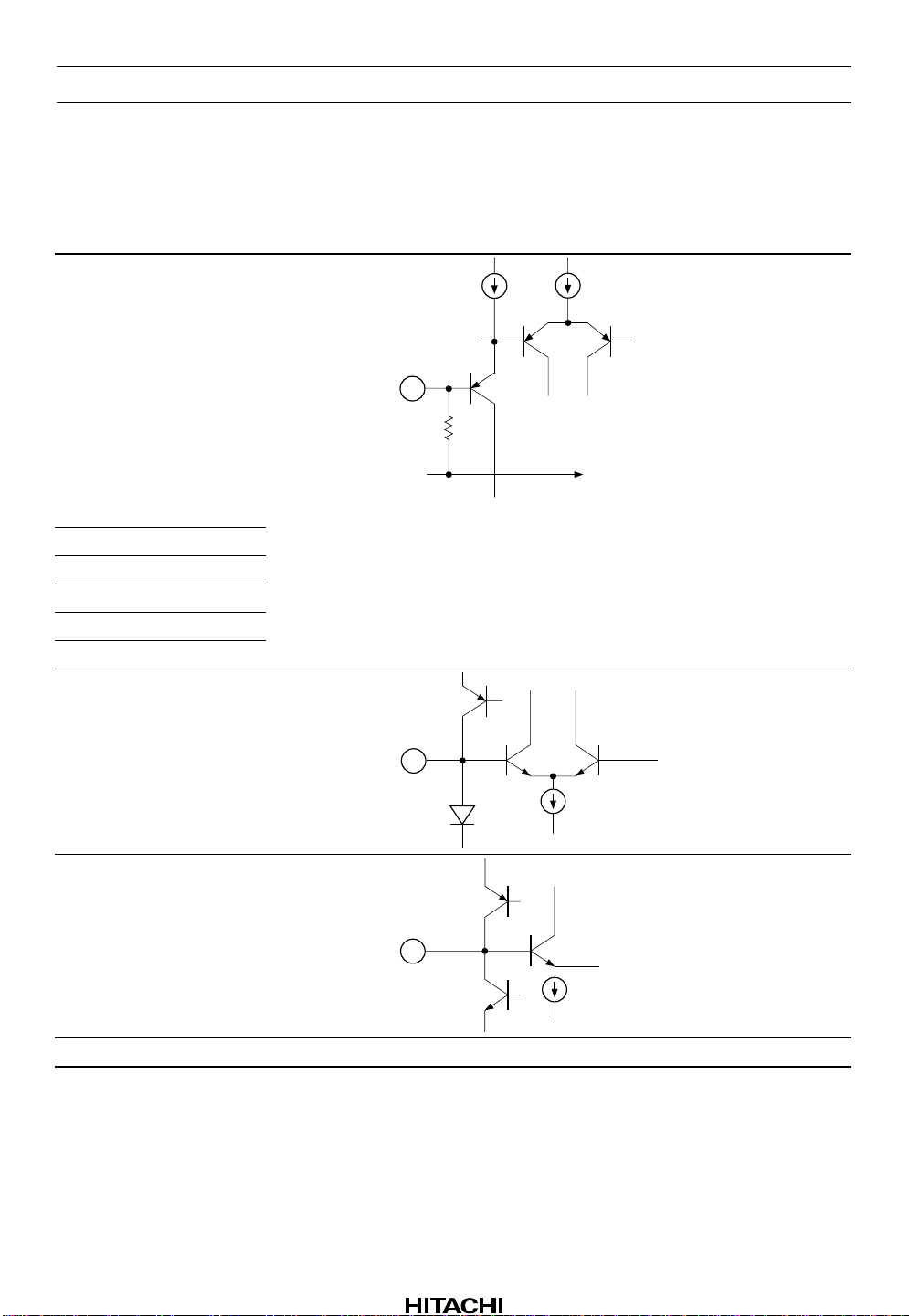
Pin Description (VCC = 9 V Single supply, Ta = 25°C, No signal, The value in the table
show typical value)
Terminal
Pin No.
2, 41 TAI 100 kΩ VCC/2
name Zin
DC
voltage Equivalent circuit Description
Tape input
VCC/ 2
4, 39 RAI Radio input
25 MSI Music sensor
rectifier input
10, 33 HLS DET — 2.5 V Time constant
pin for rectifier
11, 32 LLS DET
3 BIAS — 0.28 V
GND
Reference
current input
Rev.1, Nov. 1992, page 2 of 66
Page 3
HA12173 Series
Pin Description (VCC = 9 V Single supply, Ta = 25°C, No signal, The value in the table
show typical value) (cont)
Terminal
Pin No.
24 MS DET — V
19 MS GV 100 kΩ —
40 RIP — VCC/2 Ripple filter
name Zin
DC
voltage Equivalent circuit Description
CC
GND
DGND
GND
Time constant
pin for rectifier
Mode control
input
Rev.1, Nov. 1992, page 3 of 66
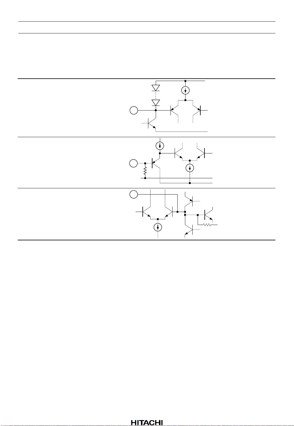
Page 4
HA12173 Series
Pin Description (VCC = 9 V Single supply, Ta = 25°C, No signal, The value in the table
show typical value) (cont)
Terminal
Pin No.
name Zin
43, 56 EQ OUT — VCC/2
DC
voltage Equivalent circuit Description
V
CC
GND
Equalizer output
6, 37 PB OUT Play back
(Decode) output
30 MS V
REF
Reference
voltage buffer
output
26 MA OUT Music sensor
amp output
47, 52 V
REF
Reference
voltage buffer
output
12, 31 REC OUT Recording
(Encode) output
8, 35 SS2 Spectral skewing
amp. output
44, 55 EQ OUT-M — VCC/2
V
CC
Equalizer output
(Metal)
Rev.1, Nov. 1992, page 4 of 66
GND
Page 5
HA12173 Series
Pin Description (VCC = 9 V Single supply, Ta = 25°C, No signal, The value in the table
show typical value) (cont)
Terminal
Pin No.
21 MS OUT — —
22 V
23 MS V
20 D GND — 0V — Digital (Logic)
27 MS GND Music sensor
49, 50 GND Ground
48, 51 FIN — VCC/2 PB - EQ input for
name Zin
CC
CC
—VCC— Power supply
DC
voltage Equivalent circuit Description
MS V
D GND
CC
Music sensor
output to MPU
ground
ground
forward
46, 53 RIN PB - EQ input for
reverse
45, 54 NFI Negative
feedback
terminal of PB EQ amp.
28 NOI Negative
feedback input
for normal speed
29 FFI Negative
feedback input
for FF or REW
Rev.1, Nov. 1992, page 5 of 66
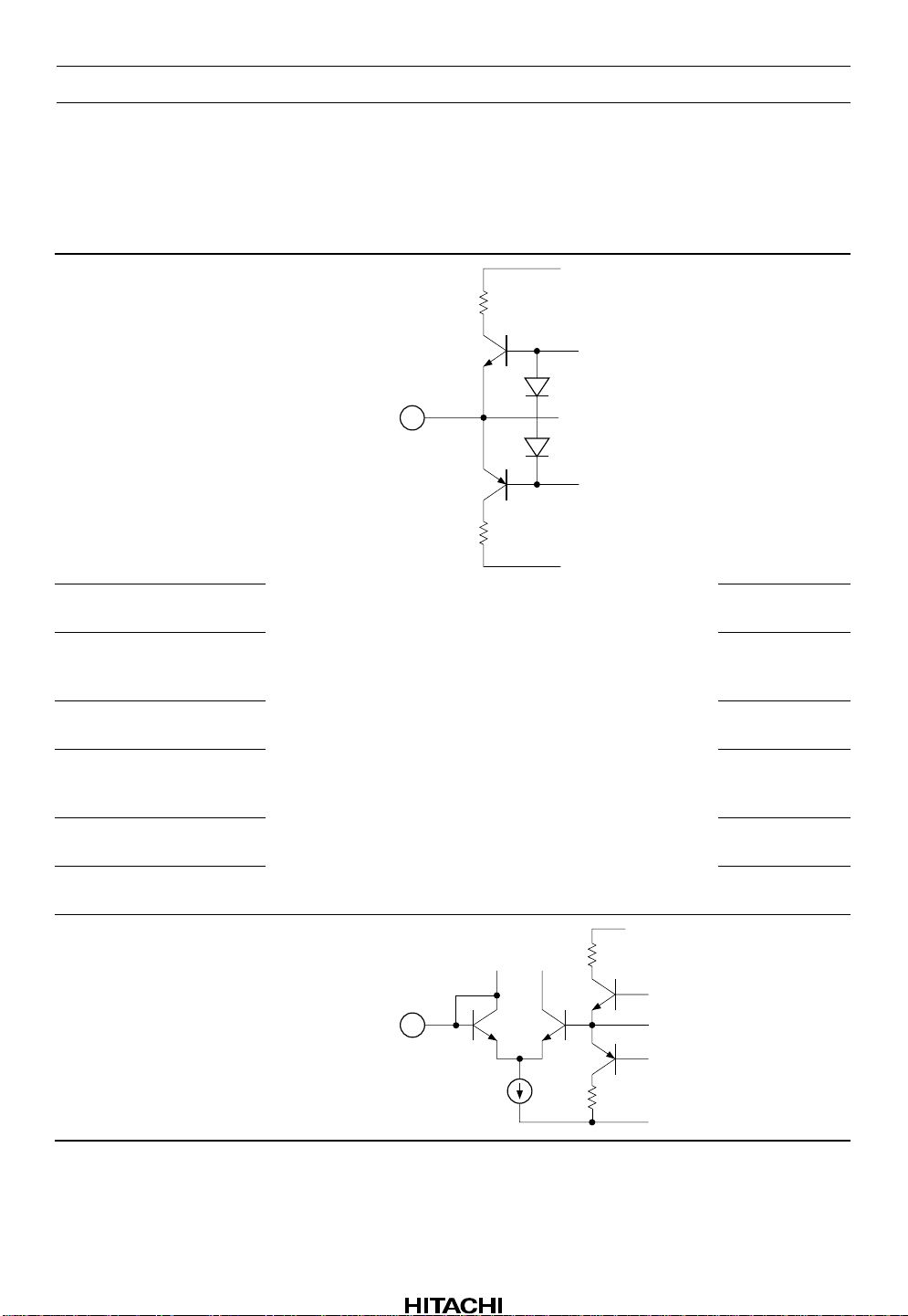
Page 6
HA12173 Series
Pin Description (VCC = 9 V Single supply, Ta = 25°C, No signal, The value in the table
show typical value) (cont)
Terminal
Pin No.
13 C/B 100 kΩ —
14 ON/OFF
15 REC/PB
16 TAPE/RADIO
17 120 µ/170 µ
18 F/R
7, 36 SS1 — VCC/2 Spectral skewing
name Zin
DC
voltage Equivalent circuit Description
Mode control
input
D GND
GND
amp. input
9, 34 CCR — VCC/2 Current
controled
resistor output
1, 5, 38, 42 NC No connection
Rev.1, Nov. 1992, page 6 of 66
Page 7
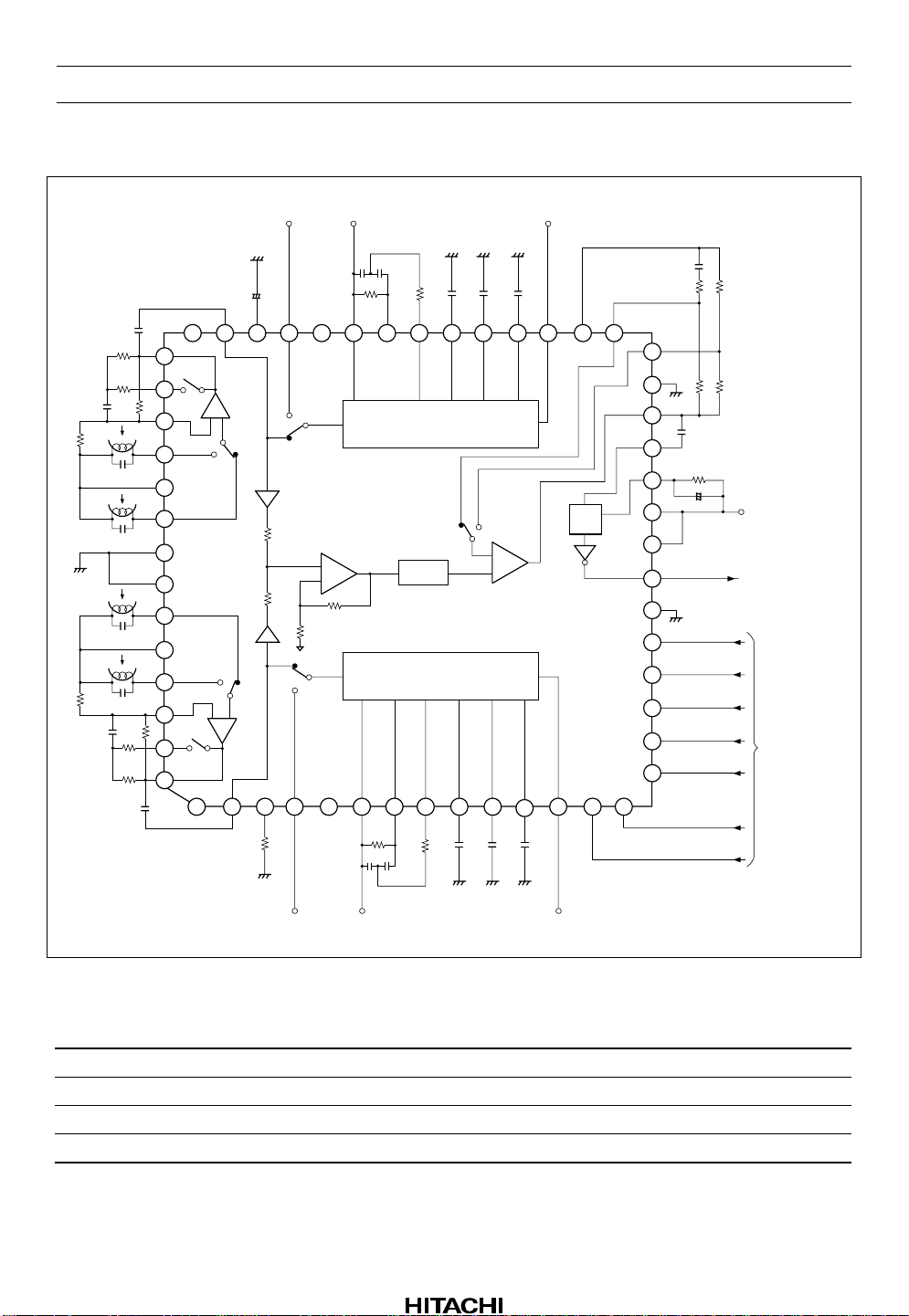
Block Diagram
HA12173 Series
RADIO
IN(L)
EQOUT(L)
42 41 40 39 38 37 30 29
43
120/70
44
45
46
V (L)
47
REF
48
GND
49
GND
50
51
V (R)
52
REF
53
54
55
120/70
56
EQOUT(R)
+
RIP
+
–
R/F
×1
×1
R/F
–
+
BIAS
T/R
T/R
PBOUT(L)
+
–
RECOUT(L)
36 35 34 33 32 31
DOLBY B/C-NR
S/R
–
LPF
+
MS AMP
DOLBY B/C-NR
968713
1110
MS VREF
DET
MS GND
MS V
CC
V
CC
D GND
141254132
C/B
28
27
26
25
24
23
22
21
20
19
18
17
16
15
ON/OFF
+
MS OUT
(S/R)
MS G
V
F/R
120 µ/70 µ
TAPE/RADIO
REC/PB
V
CC
To Microcomputer
From
Microcomputer
IN(R)
PBOUT(R)RADIO
RECOUT(R)
Absolute Maximum Ratings
Item Symbol Ratings Unit Condition
Supply voltage VCC max 16 V
Power dissipation P
T
Operating temperature Topr –40 to +85 °C
Storage temperature Tstg –55 to +125 °C
500 mW Ta≤85°C
Rev.1, Nov. 1992, page 7 of 66
Page 8
HA12173 Series
Electrical Characteristics (Ta = 25°C Dolby level 300 mVrms (Rec-out pin))
HA12173 VCC = 9.0 V HA12174 VCC = 9.0 V
HA12175 V
Item Symbol Min Typ Max Unit Test Condition Note
Quiescent current I
Q
Input HA12173 GvIA TAI 18.5 20.0 21.5 dB Vin = 0 dB, f = 1 kHz
Amp. GvIA RAI 15.5 17.0 18.5
gain HA12174 GvIA TAI 22.0 23.5 25.0 Vin = 0 dB, f = 1 kHz
GvIA RAI 19.0 20.5 22.0
HA12175 GvIA TAI 24.2 25.7 27.2 Vin = 0 dB, f = 1 kHz
GvIA RAI 21.2 22.7 24.2
HA12177 GvIA TAI 26.7 28.2 29.7 Vin = 0 dB, f = 1 kHz
GvIA RAI 23.7 25.2 26.7
B-type Encode ENC –2k 2.8 4.3 5.8 dB Vin = –20 dB, f = 2 kHz
boost ENC –5k 1.7 3.2 4.7 Vin = –20 dB, f = 5 kHz
C-type Encode ENC –1k (1) 3.9 5.9 7.9 dB Vin = –20 dB, f = 1 kHz
boost ENC –1k (2) 18.1 19.6 21.6 Vin = –60 dB, f = 1 kHz
ENC –700 9.8 11.8 13.8 Vin = –30 dB, f = 700 Hz
Signal handling Vo max 12.0 13.0 — dB THD = 1%, f = 1 kHz *1
Signal to noise
S/N 60.0 64.0 — dB Rg = 5.1 kΩ, CCIR/ARM
ratio
THD THD — 0.05 0.3 % Vin = 0 dB, f = 1 kHz
Channel CT RL (1) 70.0 85.0 — dB Vin = 0 dB, f = 1 kHz RAI input
separation CT RL (2) 50.0 60.0 — Vin = 0.6 mVrms, f = 1 kHz EQ input
Crosstalk CT EQ → RAI 70.0 80.0 — Vin = 0.6 mVrms, f = 1 kHz EQ input
CT RAI → EQ 50.0 60.0 — Vin = 0 dB, f = 1 kHz RAI input
PB - EQ gain Gv EQ 1k 37.0 40.0 43.0 dB Vin = 0.6 mVrms, f = 1 kHz 120 µ
Gv EQ 10k (1) 33.0 36.0 39.0 Vin = 0.6 mVrms, f = 10 kHz
Gv EQ 10k (2) 29.0 32.0 35.0 70 µ
PB - EQ maximum
VoM 300 600 — mVrms THD = 1%, f = 1 kHz *1
output
PB - EQ THD THD - EQ — 0.05 0.3 % Vin = 0.6 mVrms, f = 1 kHz
Noise voltage level
V
N
converted in input
MS sensing level VON (1) –36.0 –32.0 –28.0 dB f = 5 kHz, Normal speed
VON (2) –18.0 –14.0 –10.0 f = 5 kHz, High speed
10.0 16.0 24.0 mA No input No Signal
— 0.7 1.5 µVrms Rg = 680 Ω, DIN - AUDIO
= 12.0 V HA12177 VCC = 14.0 V
CC
NR-B70 µ
Rev.1, Nov. 1992, page 8 of 66
Page 9

HA12173 Series
Electrical Characteristics (Ta = 25°C Dolby level 300 mVrms (Rec-out pin)) (cont)
HA12173 VCC = 9.0 V HA12174 VCC = 9.0 V
HA12175 V
Item Symbol Min Typ Max Unit Test Condition Note
MS output low
V
OL
level
MS output leak
I
OH
current
Control voltage V
IL
V
IH
Note: 1. HA12173 VCC = 7.0 V, HA12174 VCC = 8.0 V, HA12175 VCC = 9.5 V, HA12177 VCC = 12.0 V
—1.01.5V
—0.02.0µA
–0.2 — 1.5 V
3.5 — 5.3
= 12.0 V HA12177 VCC = 14.0 V
CC
Rev.1, Nov. 1992, page 9 of 66
Page 10
HA12173 Series
Test Circuit
5 V
R29
R30
EQOUT (L)
10 k
10 k
SW22
PBOUT (L)
ON
RECOUT (L)
DC VM1
SW21
SW24
SW23
EQOUT(L)
OFF
LR
PBOUT(L)
RECOUT(L)
RAI (L)
DC SOURCE1
R27
330 k
R28
18 k
C21
2200 p
R33
5.1 k
EQIR (L)
EQIF(L)
SW25
A GND
C29
100 µ
+
CC
V
MS
+
R24
330 k
C14
0.01 µ
R25
47 k
C28
4700 p
R26
33 k
+
C15
2.2 µ
C18
2200 p
C20
2200 p
R32
+
C19
2.2 µ
+
C23
0.47 µ
R34
5.1 k
C24
0.1 µ
R35
5.1 k
R36
12 k
R38
330 k
R39
180
C25
0.01 µ
R40
680
+
R41
680
C27
22 µ
+
V
C13
0.33 µ
MS
DET
MSI
MA
OUT
MS
GND
FFI NOI
MS
VREF
REC
C16
0.1 µ
LLS
C17
0.1 µ
HLS
(L)
CCR
R31
560
(L)
SS2
(L)
SS1
22 k
PB
N.C.
(L)
RAI
+
RIP
C22
1 µ
(L)
TAI
N.C.
EQ
R37
18 k
EQ
(L)
NFI
(L)
RIN
C26
22 µ
(L)
VREF
(L)
FIN
49 48 47 46 45 44 43 42 41 40 39 38 37 36 35 3334 32 31 30 29 28 27 26 25 24 23 22
GND
Note : The capacitor (C29) should
be connected.
It's recommended to be
connected close to the IC.
MS
2120
OUT
CC
D
GND
GV
MS
1918
F/R
17
/70µ
120µ
16
TAPE/
RADIO
/PB
1514131211109876543215655545352
REC
ON/
OFF
C/B
(L)
OUT
DET
DET
OUT
(R)
REC
OUT
(L)
(R)
LLS
DET
(L)
(R)
HLS
DET
(R)
CCR
(R)
SS2
(R)
SSI
(L)
PB
(R)
OUT
N.C.
(R)
RAI
HA12173/4/5/7 (PB 1 Chip)
BIAS
(R)
TAI
N.C.
(L)
(R)
EQ
OUT
OUT
(L)
(R)
EQ
OUT-M
OUT-M
(R)
NFI
(R)
RIN
(R)
VREF
(R)
51
FIN
GND
50
R23
3.9 k
SW1SW2
R22
22 k
R21
22 k
SW3SW4
R20
22 k
R19
22 k
+
SW5SW6
R18
22 k
C33
22 µ
R17
22 k
C32
PB REC 120 µ 70 µ SER REP
22 µ
+
+
C11
0.1 µ
C10
0.1 µ
OFF ON TAP RAD FOR REV
R16
22 k
SW7
C
B
C31
22 µ
+
C12
2.2 µ
R13
560
R12
22 k
+
C8
2.2 µ
C5
0.47 µ
+
R11
18 k
C4
0.1 µ
R8
5.1 k
R7
12 k
R6
18 k
C3
0.01 µ
R2
680
++
C2
22 µ
R1
680
C1
22 µ
C7
R9
R5
R3
2200 p
5.1 k
330 k
180
EQIF(R)
SW16
SW13 SW12 SW11 SW10 SW9 SW8
SW14
C9
2200 p
C6
2200 p
EQIR (R)
RAI (R)
LR
SW15
DC SOURCE2
R10
5.1 k
ON OFF
DC SOURCE3
SW18
MSOUT
RECOUT(R)
PBOUT(R)
SW17
D GND
EQOUT(R)
AC VM1 AUDIO SG
L
R
RECOUT(R)
PBOUT(R)
SW19 SW20
EQOUT(R)
R15
R14
10 k
10 k
AC VM2
ANALYZER
DISTORTION
OSCILLO SCOPE
NOISE METER
Ω
Unit R:
C: F
Note
1) Resistor tolerance are ± 1%
2) Capacitor tolerance are ± 1%
Noise meter
with CCIR/ARM filter
and DIN-AUDIO filter
Rev.1, Nov. 1992, page 10 of 66
Page 11

HA12173 Series
Functional Description
Power Supply Range
HA12173 series are provided with four line output level, which will permit on optimum overload margin
for power supply conditions. And this series are designed to operate on either single supply or split supply.
Table 1 Supply Voltage
Item HA12173 HA12174 HA12175 HA12177
Single supply 7.0 V to 16.0 V 8.0 V to 16.0 V 9.5 V to 16.0 V 12.0 V to 16.0 V
Split supply GND level ±5.0 V to 8.0 V ±5.0 V to 8.0 V ±5.0 V to 8.0 V ±6.0 V to 8.0 V
VEE level ±3.5 V to ±8.0 V ±4.0 V to 8.0 V ±4.8 V to 8.0 V ±6.0 V to 8.0 V
A. The lower limit of supply voltage depends on the line output reference level.
The minimum value of the overload margin is specified as 12 dB by Dolby Laboratories.
B. In case of using digital GND terminal referring to GND level, operating voltage range varies
depending on the condition at power on. On using the HA12173/174/175, use within the following
ranges to avoid latch-ups.
When power on in NR-OFF mode: ±5.0 V to ±8.0 V
When power on in NR-ON mode: ±5.7 V to ±8.0 V
C. In the reverse-voltage conditions such as ‘D-GND is higher than V
GND’, excessive current flows into the D-GND to destory this IC. To prevent such destru ctio n, pa y
attention to the followings on using.
Single power supply : Short-circuit the D-GND and GND directory on the board mounting this IC.
Split power supply : Avoid reverse conditions of D-GND and V
transient-time of power ON/OFF.
’ or ‘D-GND is lower than
CC
or VEE voltage, including
CC
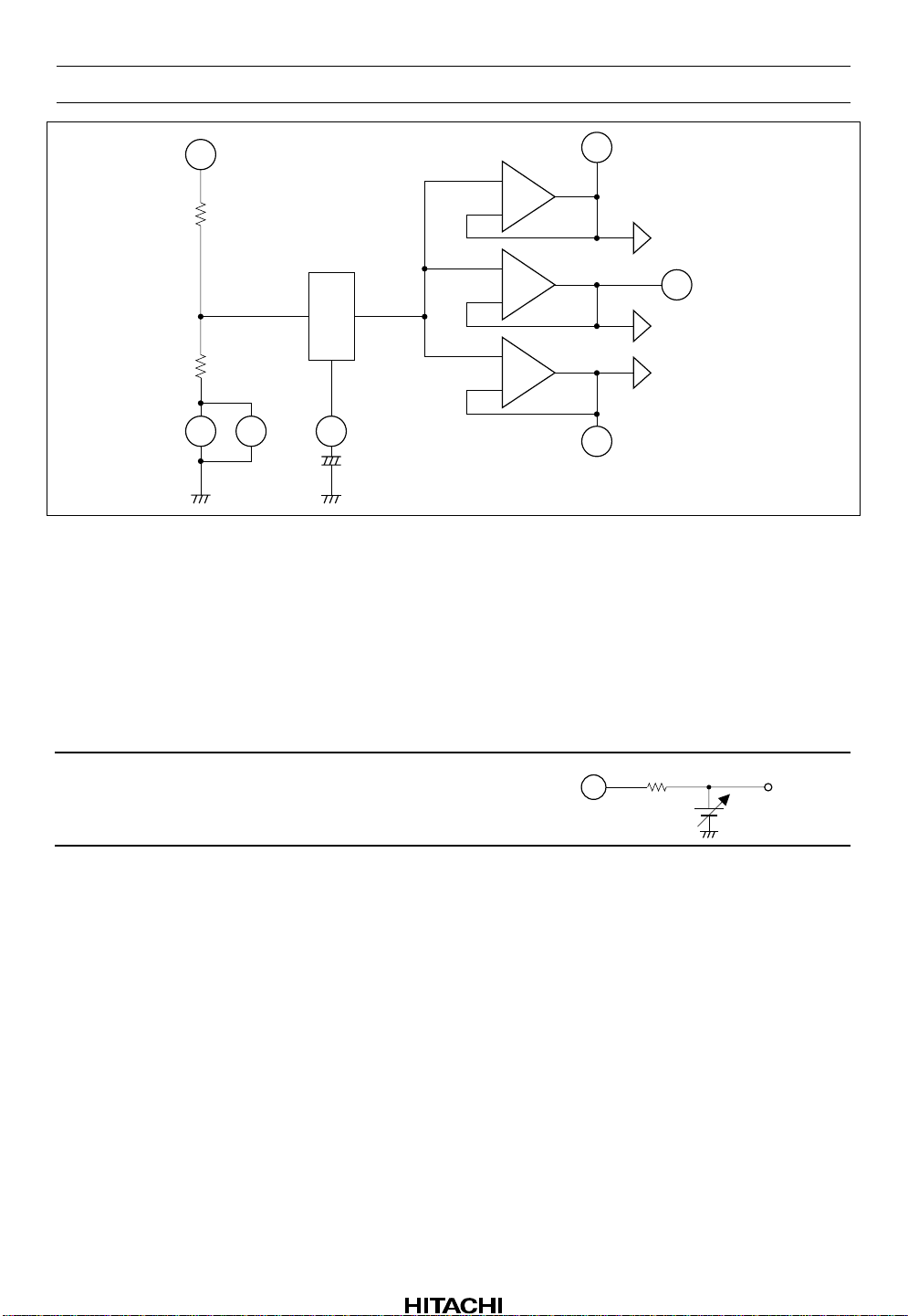
Reference Voltage
For the single supply operation these devices provide the reference voltage of half the supply voltage that is
the signal grounds. As the peculiarity of these devices, the capacitor for the ripple filter is very small about
1/100 compared with their usual value. The Reference voltage are provided for the left channel and the
right channel separately. The block diagram is shown as figure 1.
Rev.1, Nov. 1992, page 11 of 66
Page 12
HA12173 Series
22
47
V
(L)
V
CC
+
REF
RIPGND 49 50 40
+
C22
–
+
–
+
–
52
1 Fµ
L channel
reference
Music sensor
reference
R channel
reference
V
(R)
REF
MS V52
REF
Figure 1 The Block Diagram of Reference Voltage Supply
Operating Mode Control
HA12173 series provide fully electronic switching circuits. And each operating mode control are
controlled by parallel data (DC voltage).
Table 2 Threshold Voltage (V
Pin No. Low High Unit Test condition
13, 14, 15, 16,
17, 18, 19
–0.2 to 1.5 3.5 to 5.3 V
)
TH
Input Pin Measure
22 k
V
Rev.1, Nov. 1992, page 12 of 66
Page 13

HA12173 Series
Table 3 Switching Truth Table
Pin No. Low High
13 B - NR C - NR
14 NR - OFF NR - ON
15 PB REC
16 TAPE RADIO
17 120 µ (NORMAL) 70 µ (METAL or CHROME)
18 FORWARD REVERSE
19 SER (FF or REV) REP (NORMAL SPEED)
Notes: 1. Voltages shown above are determined by internal circuits of LSI when take pin 20 (DGND pin) as
reference pin. On split supply use, same V
pin.
This means that it can be controlled directly by microprocessor. But power supply should be
over ±5 V, notwithstanding the prescription of table 1.
2. Each pins are on pulled down with 100 kΩ internal resistor.
Therefore, it will be low-level when each pins are open.
3. Over shoot level and under shoot level of input signal must be the standardized (High: 5.3 V,
Low: –0.2 V)
4. When connecting microcomputer or Logic-IC with HA12173 series directly, there is apprehension
of rush-current under some transition timming of raising voltage or falling voltage at V
On using, connect protective resistors of 10 to 22 kΩ to all the control pins. It is shown is test
circuit on this data sheet. And pins fixed to low level should be preferably open.
5. Pay attention not to make digital GND voltage lower than GND voltage.
can be offered by connecting DGND pin to GND
TH
ON/OFF.
CC
Rev.1, Nov. 1992, page 13 of 66
Page 14
HA12173 Series
Input Block Diagram and Lev e l Diagram
R34
5.1 k
R35
5.1 k
EQ OUT
C24
0.1µ
HA12173: 300 mVrms (–8.2 dBs)
HA12174: 450 mVrms (–4.7 dBs)
HA12175: 580 mVrms (–2.5 dBs)
HA12177: 775 mVrms (0.0 dBs)
RAITAI PBOUT
R36
R39
180
R38
330 k
12 k
R37
18 k
C25
0.01µ
Unit R:
C: F
Ω
EQ OUT-M
EQ AMP
NFI
R
IN
V
REF
F
IN
Figure 2 Input Block Diagram
Adjustment of Playback Dolby Level
30 mVrms
(–28.2 dBs)
+–
0.6 mVrms
(–62.2 dBs)
42.4 mVrms
(–25.2 dBs)
INPUT AMP
+
NR circuit
–
The each level shown above is typical value
when offering PBOUT level to PBOUT pin.
(EQ AMP Gv = 40 dB f = 1 kHz)
RECOUT
300 mVrms
(–8.2 dBs)
After replace R34 and R35 with a half-fix volume of 10 kΩ, adjust RECOUT level to be Dolby level with
playback mode.
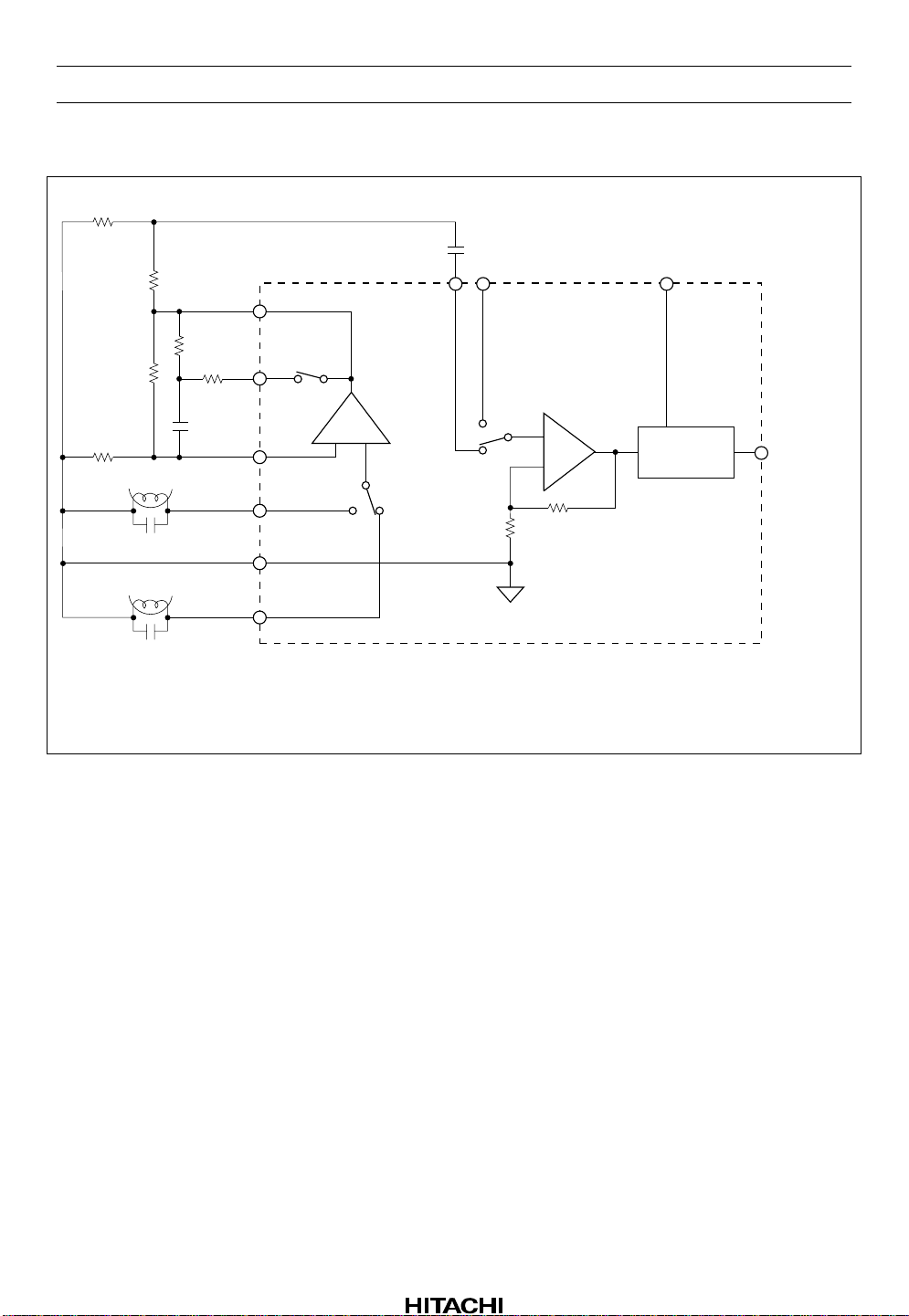
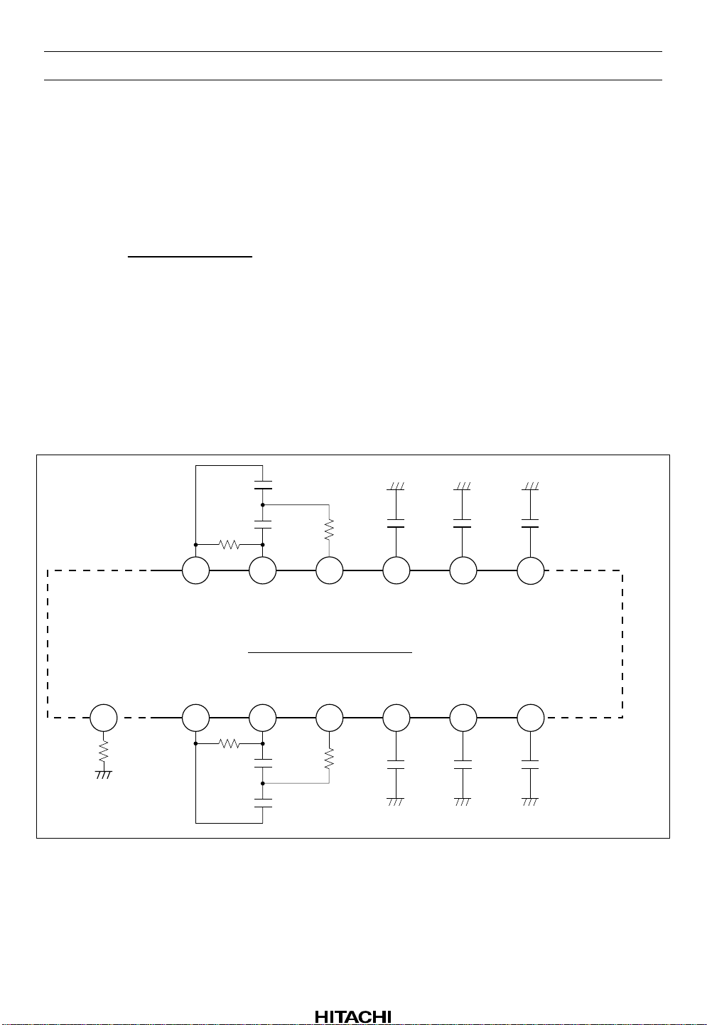
Note on Connecting with Tape Head to IC
This IC has no internal resistor to give the DC bias current to equalizer amp., therefore the DC bias current
will give through the head. This IC provides the Vref buffer output pin for Rch and Lch separ ately (has
two Vref terminal). In case of use that the Rch and Lch reference of head are connected commonly, please
use one of Vref terminals of IC (47 pin or 52 pin) for head reference. If both 47 pin and 52 pin of IC are
connected, rush current give the great damage to IC. The application circuit is shown in figure 3.
Rev.1, Nov. 1992, page 14 of 66
Page 15
43
44
HA12173 Series
45
46
47
48
49
50
51
52
53
54
55
V (L)
REF
GND
GND
V (R)
REF
–
R/F
R/F
– +
+
56
Figure 3 Application Circuit
Rev.1, Nov. 1992, page 15 of 66
Page 16
HA12173 Series
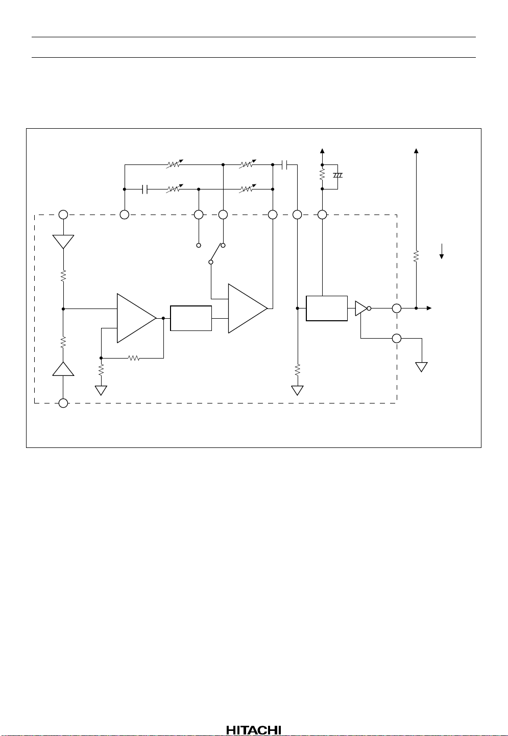
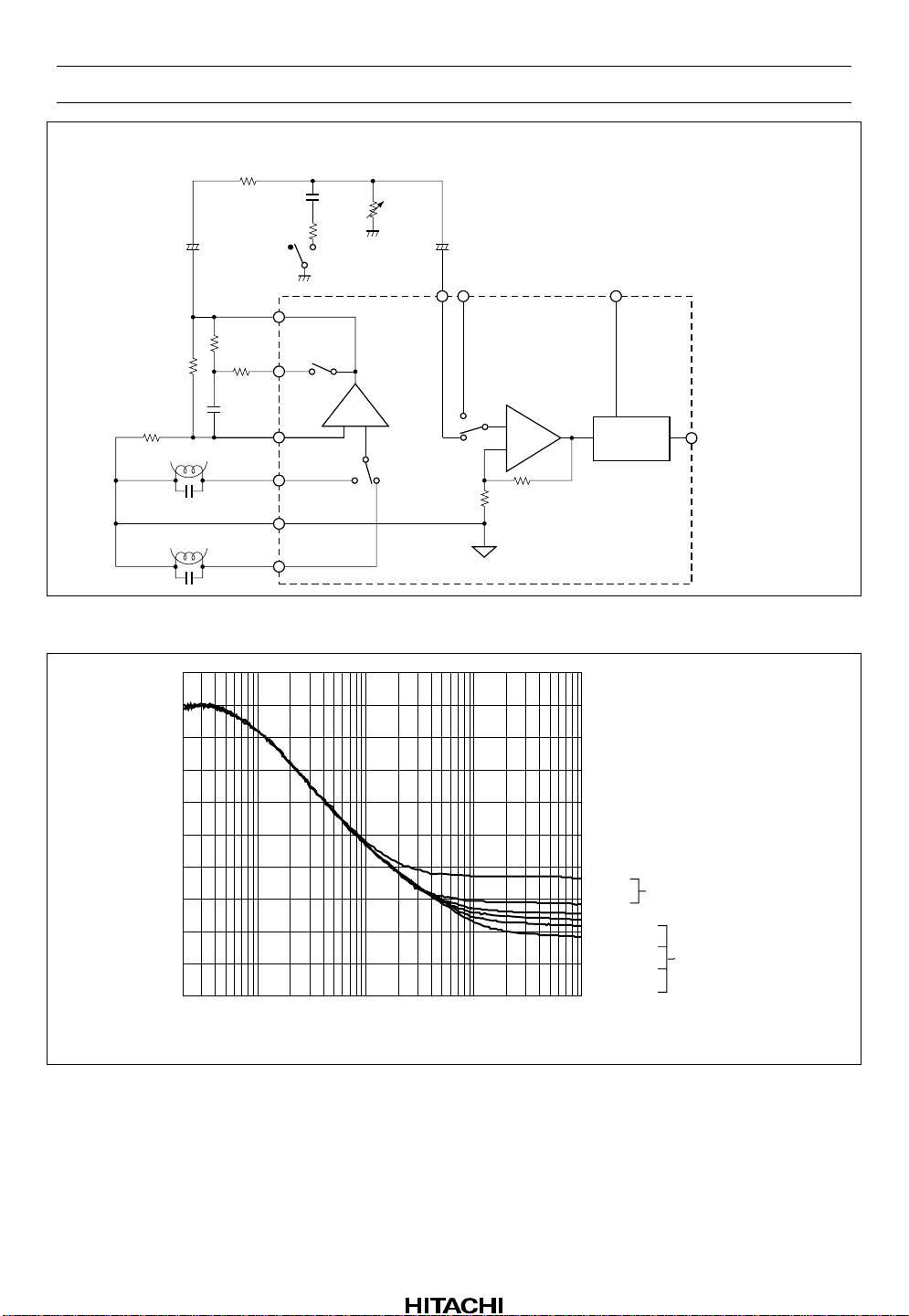
The Sensitivity Adjustment o f a Music Sensor
Adjusting MS AMP. gain by external resistor, the sensitivity of music sensor can set up.
TAI (L)
X1
–6 dB
X1
TAI (R)
R28 R27
R26 R25
C28
4700 p
MS
V
REF
L·R signal addition circuit
+
–
26 dB
LPF
25 kHz MS AMP
C14
0.01 µ
FFI NOI MA
OUT
+
–
V
CC
R24
330 k
MSI MS
DET
DET
100 k
+
C13
0.33 µ
Unit R:
MS OUT
D GND
Ω
C: F
DV
CC
I
R
L
Microcomputer
D GND
L
Rev.1, Nov. 1992, page 16 of 66
Figure 4 Music Sensor Block Diagram
Page 17
HA12173 Series
Gv1
Gv
[dB]
Gv2
1. Normal mode
Gv1 = 20log 1+
f1=
⋅π ⋅
2
R27
R28
1
C14⋅100 k
f
1
Figure 5 Frequency Response
[dB]
[Hz], f 2=25 k[Hz]
f
2
Normal speed
f
3
FF or REV
1 k10010 10 k 25 k 100 k
f [Hz]
f
4
2. FF or REW mode
R25
Gv2 = 20log 1+
=
f3
2⋅π⋅C28⋅R26
1
[dB]
R26
[Hz],f4=25k [Hz]
A standard level of TAI pin is 30 mVrms and the gain for TAI to MS AMP input is 10, therefore, the
other channel sensitivity of music sensor (S) is computed by the formula mentioned below.
S=20 log
C
30
⋅
10⋅ A
[dB]
1
A = MS AMP. gain (B dB)
S = –7.3–B [dB] C = 130 mVrms (typ.)
S is 6 dB up in case of the both channels.
C = The sensing level of music sensor
Rev.1, Nov. 1992, page 17 of 66
Page 18
HA12173 Series
Music Sensor Output (MS OUT)
As for the internal circuit of music sensor block, music sensor out pin is connected to the collector of NPN
Type directly, Output level will be “high” when sensing no sign a l. And outp ut level will be “low” when
sensing signal.
Connection with microcomputer, design I
– MSOUTLo*
DV
I
L
CC
=
R
L
at 1 mA typ.
L
* MSOUTLo: Sensing signal (about 1 V)
Notes: 1. Supply voltage of MS OUT pin must be less than V
2. MS V
pin and VCC pin are required the same voltage.
CC
voltage.
CC
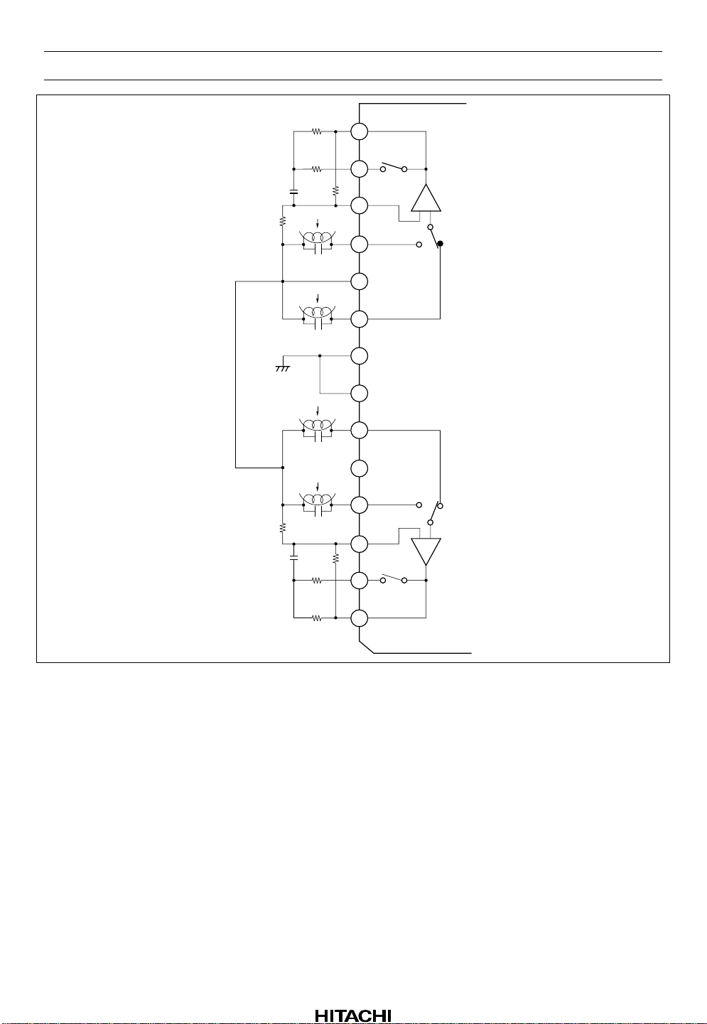
The Tolerances of External Components for Dolby NR-block
For adequate Dolby NR tracking response, take external components shown below.
C21
2200 p
SS1
(L)
±5%
C20
2200 p
±5%
SS2
(L)
R31
560
±2%
CCR
(L)
C18
2200 p
±5%
HLS
DET (L)
C17
0.1
±10%
µ
R32
22 k
±2%
37 36 35 34 33
PB OUT
(L)
32
LLS
DET (L)
C16
0.1
µ
±10%
HA12173 Series (PB 1 Chip)
3
PB OUT
(R)
67 910
R11
18 k
±2%
R12
22 k
±2%
SS1
(R)
C7
2200 p
±5%
C6
2200 p
±5%
SS2
(R)
8
R13
560
±2%
CCR
(R)
C9
2200 p
±5%
DET(R)BIAS
HLS
C10
0.1
±10%
DET(R)
µ
LLS
11
C11
0.1
µ
±10%
Unit R:
C: F
Figure 6 Tolerances of External Components
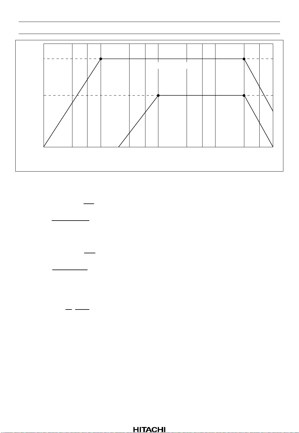
PB Equalizer for Double Speed
PB equalizer can be design for double speed by using external components shown in figure 7. Application
data is shown in figure 8.
Rev.1, Nov. 1992, page 18 of 66
Ω
Page 19
HA12173 Series
4.7
R38
330 k
R39
180
R35
5.1 k
µ
0.015
µ
+
R36
12 k
R37
18 k
C25
0.01
No
µ
R
Do
EQ OUT
EQ
OUT-M
EQ
AMP.
NFI
RIN
V
REF
FIN
– +
22 k
VR1
µ
0.1
+
TAI RAI PBOUT
INPUT AMP.
No : Normal speed
Do : Double speed
Please ajust RECOUT level to
*
be Dolby level with volume of
VR 1.
+
–
NR
circuit
RECOUT
Unit
R:
C: F
Ω
Figure 7 Application Circuit for Double Speed
60
50
40
V
G (dB)
30
20
10
20 100 1 k 10 k 100 k
Frequency (Hz)
Figure 8 Application data
µ
120
70
R = 2.7 k
R = 2.2 k
R = 1.8 k
R = 1.3 k
OUTPUT = TAIpin
*
Normal speed
µ
Double speed
Rev.1, Nov. 1992, page 19 of 66
Page 20
HA12173 Series
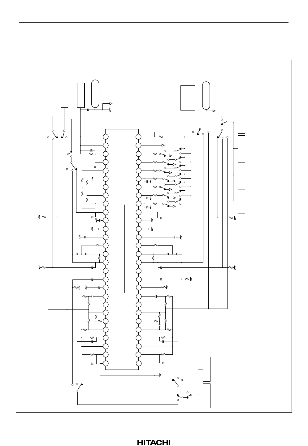
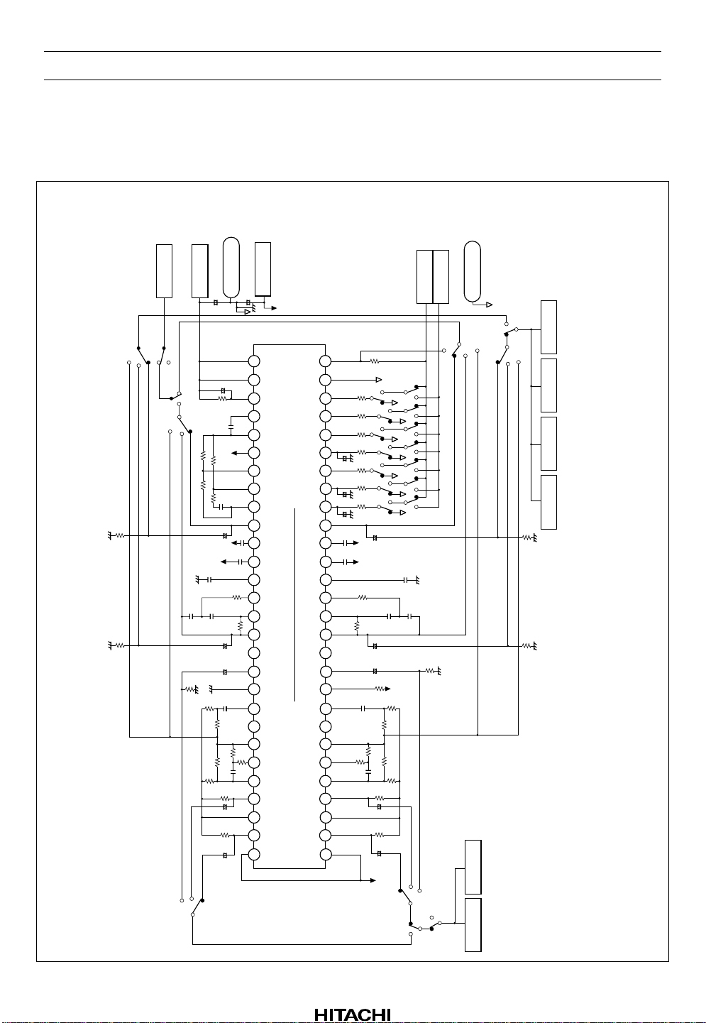
Circuit For Split Supply
HA12173
EE
EE
5 V
R29
R30
EQOUT (L)
10 k
10 k
SW22
PBOUT (L)
ON
RECOUT (L)
DC VM1
SW21
SW24
SW23
EQOUT(L)
OFF
LR
PBOUT(L)
RAI (L)
DC SOURCE1
R27
330 k
RECOUT(L)
R28
18 k
C21
2200 p
R33
5.1 k
EQIR (L)
EQIF(L)
SW25
0.33 µ
C17
+
C16
0.1 µ
560
R37
C30
100 µ
0.1 µ
18 k
EE
(V )
DC SOURCE2
CC
V
MS
V
MS
DET
MSI
MA
OUT
MS
GND
FFI NOI
MS
VREF
REC
OUT
LLS
DET
HLS
DET
(L)
CCR
(L)
SS2
(L)
SS1
PB
OUT
N.C.
(L)
RAI
RIP
(L)
TAI
N.C.
EQ
OUT
EQ
OUT-M
(L)
NFI
(L)
RIN
(L)
VREF
(L)
FIN
49 48 47 46 45 44 43 42 41 40 39 38 37 36 35 3334 32 31 30 29 28 27 26 25 24 23 22
GND
Note : In case of using digital GND
terminal referring to V level,
separate digital GND and
analog GND and connect
digital GND terminal to V .
MS
2120
OUT
CC
D
GND
GV
MS
/70µ
120µ
TAPE/
RADIO
/PB
REC
ON/
OFF
(L)
(R)
REC
OUT
(L)
(R)
LLS
DET
(L)
(R)
HLS
DET
(R)
CCR
(R)
SS2
(R)
SSI
(L)
PB
(R)
OUT
(R)
RAI
HA12173/4/5/7 (PB 1 Chip)
(R)
TAI
F/R
C/B
N.C.
BIAS
R22
22 k
1918
R21
22 k
R20
22 k
17
R19
22 k
+
16
R18
22 k
C33
22 µ
1514131211109876543215655545352
R17
22 k
C32
22 µ
+
R16
22 k
+
C31
22 µ
C11
0.1 µ
C10
0.1 µ
R13
560
R12
22 k
C8
C4
N.C.
(L)
(R)
EQ
OUT
(L)
EQ
OUT-M
NFI
RIN
VREF
FIN
R6
(R)
(R)
18 k
C3
0.01 µ
(R)
C2
(R)
(R)
GND
22 µ
51
50
D GND
DC SOURCE2
DC SOURCE3
L
SW18
PBOUT(R)
EQOUT(R)
AC VM1 AUDIO SG
R
RECOUT(R)
PBOUT(R)
MSOUT
R23
3.9 k
SW1SW2
SW3SW4
SW5SW6
PB REC 120 µ 70 µ SER REP
OFF ON TAP RAD FOR REV
SW7
C
B
+
C12
2.2 µ
C9
C7
2200 p
+
2.2 µ
C5
0.47 µ
+
R11
18 k
R9
5.1 k
0.1 µ
R8
5.1 k
R7
12 k
R5
330 k
R3
180
R2
680
++
R1
680
C1
22 µ
EQIF(R)
SW16
LR
SW13 SW12 SW11 SW10 SW9 SW8
SW14
2200 p
C6
2200 p
EQIR (R)
RAI (R)
SW15
RECOUT(R)
R10
5.1 k
ON OFF
SW17
SW19 SW20
EQOUT(R)
R15
10 k
R14
10 k
AC VM2
ANALYZER
DISTORTION
OSCILLO SCOPE
NOISE METER
Ω
Unit R:
C: F
Noise meter
with CCIR/ARM filter
and DIN-AUDIO filter
CC
(V )
A GND
C29
100 µ
+
+
C13
R24
330 k
C14
0.01 µ
R25
47 k
C28
4700 p
R26
33 k
+
C15
2.2 µ
C18
2200 p
R31
C20
2200 p
R32
22 k
+
C19
2.2 µ
+
C23
0.47 µ
R34
5.1 k
C24
0.1 µ
R35
5.1 k
R36
12 k
R38
330 k
R39
180
C25
0.01 µ
R40
680
+
C26
22 µ
R41
680
C27
22 µ
+
Rev.1, Nov. 1992, page 20 of 66
Page 21

Typical Characteristic Curves
HA12173
Quiescent Current vs. Supply Voltage
17
HA12173/174/175/177
16
NR-B (70µ)
HA12173 Series
CC
15
NR-OFF (120µ)
14
Quiescent Current I (mA)
13
6
81012141618
NR-B (120µ)
NR-C (120µ)
Supply Voltage V (V)
TAlin Input Amp. Gain vs. Frequency
22
HA12173
18
14
PBout-OFF,
RECout-OFF/B/C
CC
Gain (dB)
10
6
V = 9V
CC
PBmode
2
20 100 1 k 10 k 100 k
Frequency (Hz)
Rev.1, Nov. 1992, page 21 of 66
Page 22

HA12173 Series
RAlin Input Amp. Gain vs. Frequency
22
HA12173
18
PBout-OFF/B/C,
14
RECout-OFF
Gain (dB)
10
6
V = 9V
CC
RECmode
2
20 100 1 k 10 k 100 k
Frequency (Hz)
Rev.1, Nov. 1992, page 22 of 66
Page 23

HA12173 Series
24
HA12173
21
NR-C
V = 7 V, 9 V, 16 V
CC
18
15
12
9
6
Encode Boost (dB)
3
0
–3
–6
100
10.8
HA12173
9.6
NR-B
V = 7 V, 9 V, 16 V
8.4
7.2
CC
Encode Boost vs. Frequency (1)
Vin = –60 dB
16 V
–40 dB
7 V, 9 V
–30 dB
–20 dB
–10 dB
0 dB
300 1k 3k 10k 15k
Frequency (Hz)
Encode Boost Frequency (2)
Vin = –40 dB
–30 dB
6.0
4.8
3.6
Encode Boost (dB)
2.4
1.2
0
–1.2
100
16 V
7 V, 9 V
300 1 k 3 k 10 k 20 k
–20 dB
–10 dB
0 dB
Frequency (Hz)
Rev.1, Nov. 1992, page 23 of 66
Page 24

HA12173 Series
6
HA12173
NR-C
3
V = 7 V, 9 V, 16 V
CC
0
–3
–6
–9
–12
Decode Cut (dB)
–15
–18
–21
–24
100 300 1 k 3 k 10 k 15 k
7 V, 9 V
16 V
Vin = 0 dB
–20 dB
–30 dB
–40 dB
–60 dB
Frequency (Hz)
Decode Cut vs. Frequency (2)
1.2
Decode Cut vs. Frequency (1)
HA12173
0
–1.2
Vin = 0 dB
–10 dB
–10 dB
–2.4
–3.6
–4.8
–6.0
Decode Cut (dB)
–7.2
–8.4
–9.6
–10.8
NR-B
V = 7 V, 9 V, 16 V
100 300 1 k 3 k 10 k 20 k
Rev.1, Nov. 1992, page 24 of 66
CC
–20 dB
7 V, 9 V
16 V
–30 dB
–40 dB
Frequency (Hz)
Page 25

HA12173 Series
Maximum Output Level vs. Supply Voltage (1)
25
HA12173
T.H.D. = 1 %
0 dB = 300 mVrms
20
15
f = 1 kHz
RAIin
PBmode
PBout
NR-OFF
NR-B
NR-C
Maximum Output Level Vo max (dB)
10
6 8 10 12 14 16
Supply Voltage V (V)
CC
Maximum Output Level vs. Supply Voltage (2)
25
HA12173
T.H.D. = 1 %
0 dB = 300 mVrms
f = 1 kHz
20
15
RAIin
RECmode
RECout
NR-B
NR-OFF
NR-C
Maximum Output Level Vo max (dB)
10
6 8 10 12 14 16
Supply Voltage V (V)
CC
Signal to Noise Ratio vs. Supply Voltage (1)
100
HA12173
f = 1 kHz
CCIR / ARM
PBmode
PBout
90
80
NR-B
NR-C
NR-OFF
Signal to Noise Ratio S/N (dB)
70
6 8 10 12 14 16
Supply Voltage V (V)
CC
Signal to Noise Ratio vs. Supply Voltage (2)
90
HA12173
NR-OFF
f = 1 kHz
CCIR / ARM
RECmode
80
RECout
NR-B
70
Signal to Noise Ratio S/N (dB)
NR-C
60
6 8 10 12 14 16
Supply Voltage V (V)
CC
Rev.1, Nov. 1992, page 25 of 66
Page 26

HA12173 Series
Total Harmonic Distortion vs. Supply Voltage (1)
1.0
HA12173
0.5
RAIin
PBmode
PBout
0.2
NR-OFF
0.1
0.05
0.02
Total Harmonic Distortion T.H.D. (%)
0.01
6 8 10 12 14 16
Supply Voltage V (V)
f = 10 kHz
100 Hz
1 kHz
CC
Total Harmonic Distortion vs. Supply Voltage (3)
1.0
HA12173
0.5
0.2
RAIin
PBmode
PBout
NR-C
f = 100 Hz
Total Harmonic Distortion vs. Supply Voltage (2)
1.0
HA12173
0.5
RAIin
PBmode
0.2
0.1
0.05
0.02
Total Harmonic Distortion T.H.D. (%)
0.01
6 8 10 12 14 16
Supply Voltage V (V)
PBout
NR-B
f = 100Hz
10 kHz
1 kHz
CC
Total Harmonic Distortion vs. Supply Voltage (4)
1.0
HA12173
RAIin
0.5
RECmode
RECout
NR-OFF
0.2
0.1
0.05
0.02
Total Harmonic Distortion T.H.D. (%)
0.01
6 8 10 12 14 16
Supply Voltage V (V)
Rev.1, Nov. 1992, page 26 of 66
10 kHz
1 kHz
CC
0.1
0.05
0.02
Total Harmonic Distortion T.H.D. (%)
0.01
6 8 10 12 14 16
Supply Voltage V (V)
f = 10 kHz
100 Hz, 1 kHz
CC
Page 27

HA12173 Series
Total Harmonic Distortion vs. Supply Voltage (5)
1.0
HA12173
0.5
RAIin
RECmode
RECout
NR-B
0.2
0.1
f = 100 Hz
0.05
0.02
Total Harmonic Distortion T.H.D. (%)
0.01
6
8 10121416
Supply Voltage V (V)
1 kHz
10 kHz
CC
Total Harmonic Distortion vs. Output Level (1)
5
HA12173
V = 9 V
CC
0 dB = 300 mVrms
2
RAIin
1.0
0.5
PBmode
PBout
NR-OFF
Total Harmonic Distortion vs. Supply Voltage (6)
1.0
HA12173
0.5
0.2
0.1
0.05
RAIin
RECmode
6
RECout
NR-C
8 10121416
0.02
Total Harmonic Distortion T.H.D. (%)
0.01
Supply Voltage V (V)
f = 100 Hz
10 kHz
1 kHz
CC
0.2
0.1
0.05
Total Harmonic Distortion T.H.D. (%)
0.02
0.01
–15
f = 10 kHz
100 Hz
1 kHz
–10
–505101520
Output Level Vout (dB)
Rev.1, Nov. 1992, page 27 of 66
Page 28

HA12173 Series
Total Harmonic Distortion vs. Output Level (2)
5
HA12173
V = 9 V
CC
0 dB = 300 mVrms
2
RAIin
PBmode
1.0
PBout
NR-B
0.5
0.2
0.1
0.05
f = 100 Hz
Total Harmonic Distortion T.H.D. (%)
0.02
0.01
–15 –10
10 kHz
1 kHz
–5
0510
Output Level Vout (dB)
Total Harmonic Distortion vs. Output Level (3)
5
HA12173
V = 9 V
CC
2
0 dB = 300 mVrms
RAIin
PBmode
1.0
PBout
NR-C
0.5
0.2
0.1
f = 100 Hz
10 kHz
15
20
Total Harmonic Distortion T.H.D. (%)
Rev.1, Nov. 1992, page 28 of 66
0.05
0.02
0.01
–15 –10 –5 0 5 10 15 20
1 kHz
Output Level Vout (dB)
Page 29

Total Harmonic Distortion vs. Output Level (4)
5
HA12173
V = 9 V
CC
0 dB = 300 mVrms
2
RAIin
RECmode
1.0
RECout
NR-OFF
0.5
0.2
0.1
HA12173 Series
0.05
f = 10 kHz
Total Harmonic Distortion T.H.D. (%)
0.02
0.01
–15
–10
–5
100 Hz, 1 kHz
0510
Output Level Vout (dB)
Total Harmonic Distortion vs. Output Level (5)
5
HA12173
V = 9 V
CC
0 dB = 300 mVrms
2
RAIin
RECmode
1.0
RECout
NR-B
0.5
0.2
0.1
f = 100 Hz
0.05
Total Harmonic Distortion T.H.D. (%)
0.02
1 kHz
10 kHz
15 20
0.01
–15 –10 –50 5101520
Output Level Vout (dB)
Rev.1, Nov. 1992, page 29 of 66
Page 30

HA12173 Series
Total Harmonic Distortion vs. Output Level (6)
5
HA12173
V = 9 V
CC
0 dB = 300 mVrms
2
RAIin
RECmode
RECout
1.0
NR-C
0.5
f = 100 Hz
0.2
0.1
0.05
0.2
0.1
0.05
Total Harmonic Distortion T.H.D. (%)
0.02
0.01
–15 –10 –5 0 10 15 205
1 kHz
10 kHz
Output Level Vout (dB)
Total Harmonic Distortion vs. Frequency (1)
HA12173
RAIin
PBmode
PBout
NR-OFF
Vin = +10 dB
–10 dB
0.02
Total Harmonic Distortion T.H.D. (%)
0.01
100 200 500 1 k 5 k 10 k 20 k
Rev.1, Nov. 1992, page 30 of 66
0 dB
2 k
Frequency (Hz)
Page 31

0.2
0.1
HA12173
HA12173 Series
Total Harmonic Distortion vs. Frequency (2)
RAIin
PBmode
PBout
NR-B
0.05
0.02
Vin = +10 dB
–10 dB
0 dB
Total Harmonic Distortion T.H.D. (%)
0.01
100 200 500 1 k 2 k 5 k 10 k 20 k
Frequency (Hz)
Total Harmonic Distortion vs. Frequency (3)
5
HA12173
2
1.0
0.5
0.2
0.1
0.05
RAIin
PBmode
PBout
NR-C
Vin = +10 dB
–10 dB
Total Harmonic Distortion T.H.D. (%)
0.02
0.01
100 200 500 1 k 2 k 5 k 10 k 20 k
0 dB
Frequency (Hz)
Rev.1, Nov. 1992, page 31 of 66
Page 32

HA12173 Series
0.2
0.1
0.05
HA12173
Total Harmonic Distortion vs. Frequency (4)
RAIin
RECmode
RECout
NR-OFF
Vin = +10 dB
–10 dB
0.02
Total Harmonic Distortion T.H.D. (%)
0.01
100 200 500 1 k 2 k 5 k 10 k 20 k
Frequency (Hz)
Total Harmonic Distortion vs. Frequency (5)
0.2
HA12173
0.1
0.05
0.02
0.01
100 200 500 1 k 5 k 10 k
Total Harmonic Distortion T.H.D. (%)
Vin = +10 dB
–10 dB
0 dB
2 k
Frequency (Hz)
0 dB
RAIin
RECmode
RECout
NR-B
20 k
Rev.1, Nov. 1992, page 32 of 66
Page 33

1.0
0.5
0.2
5
2
HA12173 Series
Total Harmonic Distortion vs. Frequency (6)
HA12173
RAIin
RECmode
RECout
NR-C
Vin = +10 dB
0.1
0.05
–10 dB
0 dB
Total Harmonic Distortion T.H.D. (%)
0.02
0.01
100 200 500 1 k 2 k 5 k 10 k 20 k
Frequency (Hz)
Crosstalk vs. Frequency (1)
–20
HA12173
V = 9V
CC
Radio Tape
–40
–60
–80
Crosstalk (dB)
PBmode
PBout
NR-OFF
NR-B
NR-C
–100
–120
20 50 100 200 500 1 k 2 k 5 k 10 k 20 k
Frequency (Hz)
Rev.1, Nov. 1992, page 33 of 66
Page 34

HA12173 Series
–20
HA12173
–40
–60
–80
Crosstalk (dB)
–100
–120
20
–20
HA12173
Crosstalk vs. Frequency (2)
V = 9V
CC
Radio Tape
RECmode
RECout
NR-C
NR-B
NR-OFF
50 100 200 500 1 k 2 k 5 k 10 k 20 k
Frequency (Hz)
Crosstalk vs. Frequency (3)
V = 9 V
CC
–40
–60
–80
Crosstalk (dB)
–100
–120
20 50 100 200 500 1 k 2 k 5 k 10 k 20 k
L R
RAIin
PBmode
PBout
NR-C
NR-B
NR-OFF
Frequency (Hz)
Rev.1, Nov. 1992, page 34 of 66
Page 35

HA12173 Series
–20
HA12173
V = 9 V
CC
–40
–60
–80
Crosstalk (dB)
–100
–120
20 50 100 200 500 1 k 2 k 5 k 10 k 20 k
R L
RAIin
PBmode
PBout
Frequency (Hz)
Crosstalk vs. Frequency (5)
–20
HA12173
V = 9 V
CC
Tape Radio
PBmode
–40
PBout
Crosstalk vs. Frequency (4)
NR-C
NR-OFF
NR-B
–60
–80
Crosstalk (dB)
–100
–120
20 50 100 200 500 20 k10 k5 k2 k1 k
NR-OFF
NR-B
NR-C
Frequency (Hz)
Rev.1, Nov. 1992, page 35 of 66
Page 36

HA12173 Series
–20
HA12173
–40
–60
–80
Crosstalk (dB)
–100
–120
20
–20
HA12173
–40
Crosstalk vs. Frequency (6)
V = 9 V
CC
Forward Reverse
PBmode
PBout
NR-OFF
NR-B
NR-C
50 100 200 500 1 k 2 k 5 k 10 k 20 k
Frequency (Hz)
Crosstalk vs. Frequency (7)
V = 9 V
CC
Reverse Forward
PBmode
PBout
–60
–80
Crosstalk (dB)
–100
–120
20 50 100 200 500 1 k 2 k 5 k 10 k 20 k
Rev.1, Nov. 1992, page 36 of 66
NR-OFF
NR-B
NR-C
Frequency (Hz)
Page 37

HA12173 Series
0
HA12173
–20
–40
–60
Crosstalk (dB)
–80
–100
20 50 100 200 500 1 k 2 k 5 k 10 k 20 k
Crosstalk vs. Frequency (8)
NR-OFF
NR-B
NR-C
V = 9 V
CC
L R
PBmode
PBout
Frequency (Hz)
Crosstalk vs. Frequency (9)
0
HA12173
V = 9 V
CC
–20
–40
NR-OFF
–60
Crosstalk (dB)
–80
–100
20 50 100 200 500 1 k 2 k 5 k 10 k 20 k
NR-B
NR-C
R L
PBmode
PBout
Frequency (Hz)
Rev.1, Nov. 1992, page 37 of 66
Page 38

HA12173 Series
–20
–40
0
HA12173
Ripple Rejection Ratio vs. Frequency
PBmode
PBout
NR-C
NR-OFF
–60
–80
Ripple Rejection Ratio R.R.R. (dB)
–100
20 50 100 200 500 1 k 2 k 5 k 10 k 20 k
Frequency (Hz)
EQ-AMP. Gain vs. Frequency
70
HA12173/174/175/177
V = 9 V
60
50
CC
Gain (dB)
40
NR-B
120 µ
30
20
20
Rev.1, Nov. 1992, page 38 of 66
70 µ
50 100 200 500 1 k 2 k 5 k 10 k 20 k 50 k 100 k
Frequency (Hz)
Page 39

HA12173 Series
EQOUT Maximum Output Level vs.
Supply Voltage
40
HA12173/174/175/177
EQin EQout
0 dB = 60 mVrms (EQout)
f = 1 kHz
T.H.D. = 1%
35
30
Maximum Output Voltage Vo max (dB)
25
6 8 10 12 14 16
Supply Voltage V (V)
CC
Signal to Noise Ratio vs. Supply Voltage
65
HA12173
60
55
NR-C(70µ)
NR-C(120µ)
NR-B(70µ)
NR-B(120µ)
NR-OFF(70µ)
NR-OFF(120µ)
Signal to Noise Ratio S/N (dB)
PBmode
PBout
DIN-AUDIO
f = 1 kHz
0 dB = 300 mVrms
50
6 8 10 12 14 16
Supply Voltage V (V)
CC
Total Harmonic Distortion vs.
Supply Voltage
1.0
HA12173
NR-C (70µ, 120µ)
0.1
Tortal Harmonic Distortion (%)
0.01
6 8 10 12 14 16
Supply Voltage V (V)
f = 1 kHz
Vin = +6 dB
EQin PBout
NR-OFF (120µ)
NR-OFF (70µ)
NR-B (120µ)
NR-B (70µ)
CC
Rev.1, Nov. 1992, page 39 of 66
Page 40

HA12173 Series
EQOUT, PBOUT T.H.D. vs. Output Voltage
(EQin EQOUT, PBOUT)
5
: PBmode PBout NR-OFF
: PBmode PBout NR-B
: PBmode PBout NR-C
: PBmode PBout NR-OFF
: PBmode PBout NR-B
: PBmode PBout NR-C
10
1
—
EQout
—
EQout
1
1
2
2
1
2
0.1
:
2
:
1
2
EQOUT, PBOUT T.H.D. (%)
HA12173
V = 9 V
CC
f = 1kHz
120µ
120µ
120µ
70µ
70µ
70µ
—
120µ
—
70µ
1
2
1
2
1
1
2
2
0.01
–20 –10 0 10 20 30
Output Voltage (dB)
0 dB =
300 mVrms
(PBout)
1
2
0 dB =
60 mVrms
1
(EQout)
2
1
2
2
1
0.5
HA12173
V = 9 V
CC
EQin PBout
0.2
0.1
0.05
PBmode
NR-OFF (120µ)
NR-OFF (70µ)
NR-ON (120µ)
NR-ON (70µ)
0.02
Total Harmonic Distortion (%)
0.01
20 50 100 200 500 1 k 2 k 5 k 10 k 20 k
Frequency (Hz)
Total Harmonic Distortion vs. Frequency
Rev.1, Nov. 1992, page 40 of 66
Page 41

50
HA12173/174/175/177
MAOUTout
40
HA12173 Series
MS-AMP. Gain vs. Frequency
MSIout
30
MAOUTout
Gain (dB)
20
10
0
20 50 100 200 500 1 k 2 k 5 k 10 k 20 k 50 k 100 k
MSIout
Frequency (Hz)
MS Sensing Level vs. Frequency
15
HA12173/174/175/177
5
–5
Normal
FF or REV
–15
FF or REW
MS Sensing Level (dB)
–25
Normal
–35
10 20 50 100 200 500 1 k 2 k 5 k 10 k 20 k 50 k 100 k
Frequency (Hz)
Rev.1, Nov. 1992, page 41 of 66
Page 42

HA12173 Series
Signal Sensing Time vs. Resistance
500
HA12173/174/175/177
V = 9 V
CC
f = 5 kHz
200
100
TAI 41 MSout 21
REPmode
: 0 dB
: –20 dB
0 dB : 300 mVrms
50
Signal Sensing Time (ms)
20
10
50 k 100 k 200 k 500 k 1 M
PBout
MSout
V
CC
C13
0.33
MS DET
22
24
+
m
Resistance R24 ( ) W
Signal Sensing Time vs. Capacitance
50
HA12173/174/175/177
V = 9 V
CC
f = 5 kHz
20
TAI 41 MSout 21
REPmode
10
5
2
1.0
Signal Sensing Time (ms)
0.5
0.2
0.01 0.1 0.5
: 0 dB
: –20 dB
: –30 dB
0 dB = 300 mVrms
PBout
MSout
22
C13
24
+
Capacitance C13 ( F)m
R24
R24
330 k
Rev.1, Nov. 1992, page 42 of 66
Page 43

HA12174
TAlin Input Amp. Gain vs. Frequency
26
HA12174
PBout-OFF
22
RECout-OFF/B/C
18
Gain (dB)
14
V = 9 V
CC
10
6
20 100 1 k 10 k 100 k
PBmode
Frequency (Hz)
HA12173 Series
RAlin Input Amp. Gain vs. Frequency
26
HA12174
22
18
PBout-OFF/B/C
RECout-OFF
Gain (dB)
14
V = 9 V
10
6
20 100 1 k 10 k 100 k
CC
RECmode
Frequency (Hz)
Rev.1, Nov. 1992, page 43 of 66
Page 44

HA12173 Series
24
HA12174
21
NR-C
V = 8 V, 9 V, 16 V
CC
18
15
12
9
6
Encode Boost (dB)
3
0
–3
–6
100
10.8
HA12174
9.6
NR-B
V = 8 V, 9 V, 16 V
8.4
7.2
CC
Encode Boost vs. Frequency (1)
Vin = –60 dB
16 V
–40 dB
8 V, 9 V
–30 dB
–20 dB
–10 dB
0 dB
300 1 k 3 k 10 k 15 k
Frequency (Hz)
Encode Boost vs. Frequency (2)
Vin = –40 dB
–30 dB
6.0
4.8
3.6
Encode Boost (dB)
2.4
1.2
0
–1.2
100
Rev.1, Nov. 1992, page 44 of 66
16 V
8 V, 9 V
300 1 k 3 k 10 k 20 k
–20 dB
–10 dB
0 dB
Frequency (Hz)
Page 45

HA12173 Series
6
HA12174
3
NR-C
V = 8 V, 9 V, 16 V
CC
0
–3
–6
–9
–12
Decode Cut (dB)
–15
–18
–21
–24
100 300 1 k 3 k 10 k 15 k
8 V, 9 V
16 V
Vin = 0 dB
–20 dB
–30 dB
–40 dB
–60 dB
Frequency (Hz)
Decode Cut vs. Frequency (1)
1.2
HA12174
0
–1.2
Decode Cut vs. Frequency (2)
Vin = 0 dB
–10 dB
–10 dB
–2.4
–3.6
–4.8
–6.0
8 V, 9 V
16 V
–20 dB
Decode Cut (dB)
–7.2
–8.4
–9.6
–10.8
NR-B
V = 8 V, 9 V, 16 V
CC
100 300 1 k 3 k 10 k 20 k
Frequency (Hz)
Rev.1, Nov. 1992, page 45 of 66
–30 dB
–40 dB
Page 46

HA12173 Series
Maximum Output Level vs.
Supply Voltage (1)
25
HA12174
T.H.D. = 1 %
0 dB = 450 mVrms
f = 1 kHz
RAIin
PBmode
PBout
20
NR-B,NB-OFF
NR-C
15
Maximum Output Level Vo max (dB)
10
6
810121416
Supply Voltage V (V)
CC
Maximum Output Level vs.
Supply Voltage (2)
25
HA12174
T.H.D. = 1 %
0 dB = 300 mVrms
f = 1 kHz
RAIin
RECmode
RECout
20
NR-B,NB-OFF
NR-C
15
Maximum Output Level Vo max (dB)
10
6
810121416
Supply Voltage V (V)
CC
Signal to Noise Ratio vs. Supply Voltage (1)
100
HA12174
f = 1 kHz
CCIR/ARM
PBmode
PBout
90
80
NR-C
NR-B
NR-OFF
Signal to Noise Ratio S/N (dB)
70
6
810121416
Supply Voltage V (V)
CC
Signal to Noise Ratio vs. Supply Voltage (2)
90
HA12174
NR-OFF
f = 1 kHz
CCIR/ARM
RECmode
80
RECout
NR-B
70
Signal to Noise Ratio S/N (dB)
NR-C
60
6
810121416
Supply Voltage V (V)
CC
Rev.1, Nov. 1992, page 46 of 66
Page 47

Total Harmonic Distortion vs. Output Level (1)
5
HA12174
V = 9 V
CC
0 dB = 450 mVrms
2
RAIin
PBmode
1.0
PBout
NR-OFF
0.5
0.2
f = 100 Hz
0.1
0.05
10 kHz
1 kHz
Total Harmonic Distortion T.H.D. (%)
0.02
HA12173 Series
0.01
–15
–10
–505101520
Output Level Vout (dB)
Total Harmonic Distortion vs. Output Level (2)
5
HA12174
V = 9 V
CC
0 dB = 450 mVrms
2
RAIin
PBmode
PBout
1.0
NR-B
0.5
0.2
f = 100 Hz
0.1
0.05
1 kHz
10 kHz
Total Harmonic Distortion T.H.D. (%)
0.02
0.01
–15
–10
–505101520
Output Level Vout (dB)
Rev.1, Nov. 1992, page 47 of 66
Page 48

HA12173 Series
Total Harmonic Distortion vs. Output Level (3)
5
HA12174
V = 9 V
CC
2
0 dB = 450 dB
RAIin
PBmode
1.0
PBout
NR-C
0.5
f = 100 Hz
0.2
0.1
0.05
Total Harmonic Distortion T.H.D. (%)
0.02
0.01
–15
–10
10 kHz
1 kHz
–505101520
Output Level Vout (dB)
Total Harmonic Distortion vs. Output Level (4)
5
HA12174
V = 9 V
CC
0 dB = 300 mVrms
2
RAIin
RECmode
RECout
1.0
NR-OFF
0.5
0.2
0.1
0.05
f = 100 Hz
10 kHz
Total Harmonic Distortion T.H.D. (%)
0.02
0.01
–15
–10
1 kHz
–505101520
Output Level Vout (dB)
Rev.1, Nov. 1992, page 48 of 66
Page 49

Total Harmonic Distortion vs. Output Level (5)
5
HA12174
V = 9 V
CC
0 dB = 300 mVrms
2
RAIin
RECmode
RECout
1.0
NR-B
0.5
HA12173 Series
0.2
0.1
0.05
f = 100 Hz
1 kHz
10 kHz
Total Harmonic Distortion T.H.D. (%)
0.02
0.01
–15
–10
–505101520
Output Level Vout (dB)
Total Harmonic Distortion vs. Output Level (6)
5
HA12174
V = 9 V
CC
0 dB = 300 mVrms
2
RAIin
RECmode
RECout
1.0
NR-C
0.5
0.2
f = 100 Hz
10 kHz
0.1
0.05
1 kHz
Total Harmonic Distortion T.H.D. (%)
0.02
0.01
–15
–10
–505101520
Output Level Vout (dB)
Rev.1, Nov. 1992, page 49 of 66
Page 50

HA12173 Series
–20
–40
0
HA12174
Ripple Rejection Ratio vs. Frequency
PBmode
PBout
NR-C
NR-OFF
HA12175
–60
–80
Ripple Rejection Ratio R.R.R. (dB)
–100
20 50 100 200 500 1 k 2 k 5 k 10 k 20 k
Frequency (Hz)
TAlin Input Amp. Gain vs. Frequency
28
HA12175
24
20
PBout-OFF
RECout-OFF/B/C
NR-B
Gain (dB)
Rev.1, Nov. 1992, page 50 of 66
16
V = 12 V
CC
12
8
20 100 1 k 10 k 100 k
PBmode
Frequency (Hz)
Page 51

RAlin Input Amp. Gain vs. Frequency
28
HA12175
HA12173 Series
24
20
Gain (dB)
16
12
8
20 100 1 k 10 k 100 k
24
HA12175
21
NR-C
V = 9.5 V, 12 V, 16V
18
CC
PBout-OFF/B/C
RECout-OFF
V = 12 V
CC
RECmode
Frequency (Hz)
Encode Boost vs. Frequency (1)
16 V
Vin = –60 dB
15
12
9
6
Encode Boost (dB)
3
0
–3
–6
100
–40 dB
9.5 V, 12 V
–30 dB
–20 dB
–10 dB
0 dB
300 1k 3k 10k 15k
Frequency (Hz)
Rev.1, Nov. 1992, page 51 of 66
Page 52

HA12173 Series
10.8
HA12175
9.6
NR-B
V = 9.5 V, 12 V, 16 V
8.4
7.2
6.0
4.8
3.6
Encode Boost (dB)
2.4
1.2
–1.2
3
–3
CC
0
100
6
HA12175
NR-C
V = 9.5 V, 12 V, 16 V
CC
0
Encode Boost vs. Frequency (2)
Vin = –40 dB
–30 dB
16 V
9.5 V, 12 V
300 1k 3k 10k 20k
–20 dB
–10 dB
0 dB
Frequency (Hz)
Decode Cut vs. Frequency (1)
Vin = 0 dB
–10 dB
–20 dB
–6
–9
–12
Decode Cut (dB)
–15
–18
–21
–24
100 300 1 k 3 k 10 k 15 k
Rev.1, Nov. 1992, page 52 of 66
16 V
9.5 V, 12V
Frequency (Hz)
–30 dB
–40 dB
–60 dB
Page 53

HA12173 Series
1.2
HA12175
0
–1.2
–2.4
–3.6
–4.8
–6.0
Decode Cut vs. Frequency (2)
9.5 V, 12 V
16 V
Decode Cut (dB)
–7.2
–8.4
–9.6
–10.8
NR-B
V = 9.5 V, 12 V, 16 V
CC
100 300 1 k 3 k 10 k 20 k
Frequency (Hz)
Maximum Output Level vs.
Supply Voltage (1)
25
HA12175
T.H.D. = 1 %
0 dB = 580 mVrms
f = 1 kHz
RAIin
PBmode
PBout
20
Maximum Output Level vs.
Supply Voltage (2)
25
HA12175
T.H.D. = 1 %
0 dB = 300 mVrms
f = 1 kHz
RAIin
RECmode
RECout
20
Vin = 0 dB
–10 dB
–20 dB
–30 dB
–40 dB
NR-B, NR-OFF
NR-C
15
Maximum Output Level Vo max (dB)
10
810121416
Supply Voltage V (V)
CC
NR-C
NR-B, NR-OFF
15
Maximum Output Level Vo max (dB)
10
810121416
Supply Voltage V (V)
CC
Rev.1, Nov. 1992, page 53 of 66
Page 54

HA12173 Series
Signal to Noise Ratio vs.
Supply Voltage (1)
100
HA12175
f = 1 kHz
CCIR/ARM
PBmode
PBout
90
80
NR-C
NR-B
NR-OFF
Signal to Noise Ratio S/N (dB)
70
810121416
Supply Voltage V (V)
CC
Signal to Noise Ratio vs.
Supply Voltage (2)
90
HA12175
NR-OFF
f = 1 kHz
CCIR/ARM
80
RECmode
RECout
NR-B
70
Signal to Noise Ratio S/N (dB)
NR-C
60
8 10121416
Supply Voltage V (V)
CC
Total Harmonic Distortion vs. Output Level (1)
5
HA12175
V = 12 V
CC
0 dB = 580 mVrms
2
RAIin
PBmode
1.0
PBout
NR-OFF
0.5
0.2
0.1
0.05
f = 10 kHz
100 Hz
Total Harmonic Distortion T.H.D. (%)
0.02
0.01
–15
–10
1 kHz
–505101520
Output Level Vout (dB)
Rev.1, Nov. 1992, page 54 of 66
Page 55

Total Harmonic Distortion vs. Output Level (2)
5
HA12175
V = 12 V
CC
0 dB = 580 mVrms
2
RAIin
PBmode
PBout
1.0
NR-B
0.5
0.2
0.1
f = 100 Hz
0.05
10 kHz
Total Harmonic Distortion T.H.D. (%)
0.02
1 kHz
HA12173 Series
0.01
–15
–10
–505101520
Output Level Vout (dB)
Total Harmonic Distortion vs. Output Level (3)
5
HA12175
V = 12 V
CC
0 dB = 580 mVrms
2
RAIin
PBmode
PBout
1.0
NR-C
0.5
0.2
0.1
0.05
f = 100 Hz
10 kHz
1 kHz
Total Harmonic Distortion T.H.D. (%)
0.02
0.01
–15
–10
–505101520
Output Level Vout (dB)
Rev.1, Nov. 1992, page 55 of 66
Page 56

HA12173 Series
Total Harmonic Distortion vs. Output Level (4)
5
HA12175
V = 12 V
CC
0 dB = 300 mVrms
2
RAIin
RECmode
RECout
1.0
NR-OFF
0.5
0.2
0.1
0.05
Total Harmonic Distortion T.H.D. (%)
0.02
0.01
–15
f = 100 Hz
10 kHz
1 kHz
–10
–505101520
Output Level Vout (dB)
Total Harmonic Distortion vs. Output Level (5)
5
HA12175
V = 12 V
CC
0 dB = 300 mVrms
2
RAIin
RECmode
1.0
RECout
NR-B
0.5
0.2
f = 100 Hz
0.1
0.05
1 kHz
10 kHz
Total Harmonic Distortion T.H.D. (%)
0.02
Rev.1, Nov. 1992, page 56 of 66
0.01
–15
–10
–505101520
Output Level Vout (dB)
Page 57

Total Harmonic Distortion vs. Output Level (6)
5
HA12175
V = 12 V
CC
0 dB = 300 mVrms
2
RAIin
RECmode
RECout
1.0
NR-C
0.5
f = 100 Hz
HA12173 Series
–20
–40
0.2
0.1
0.05
10 kHz
Total Harmonic Distortion T.H.D. (%)
0.02
0.01
–15
–10
–505101520
Output Level Vout (dB)
Ripple Rejection Ratio vs. Frequency
0
HA12175
PBmode
PBout
1 kHz
NR-C
NR-OFF
–60
–80
Ripple Rejection Ratio R.R.R. (dB)
–100
20 50 100 200 500 1 k 2 k 5 k 10 k 20 k
Frequency (Hz)
Rev.1, Nov. 1992, page 57 of 66
NR-B
Page 58

HA12173 Series
HA12177
TAlin Input Amp. Gain vs. Frequency
30
HA12177
PBout-OFF
26
22
RECout-OFF/B/C
Gain (dB)
18
14
V = 14 V
CC
PBmode
10
20 100 1 k 10 k 100 k
Frequency (Hz)
RAlin Input Amp. Gain vs. Frequency
30
HA12177
26
22
PBout-OFF/B/C
Gain (dB)
18
14
10
20 100 1 k 10 k 100 k
RECout-OFF
V = 14 V
CC
RECmode
Frequency (Hz)
Rev.1, Nov. 1992, page 58 of 66
Page 59

HA12173 Series
24
HA12177
21
NR-C
V = 12 V, 14 V, 16 V
CC
18
15
12
9
6
Encode Boost (dB)
3
0
–3
–6
100
10.8
HA12177
9.6
NR-B
V = 12 V, 14 V, 16 V
CC
8.4
7.2
Encode Boost vs. Frequency (1)
Vin = –60 dB
–40 dB
16 V
–30 dB
12 V, 14 V
–20 dB
–10 dB
0 dB
300 1 k 3 k 10 k 15 k
Frequency (Hz)
Encode Boost vs. Frequency (2)
Vin = –40 dB
–30 dB
6.0
4.8
3.6
Encode Boost (dB)
2.4
1.2
0
–1.2
100
16 V
12 V, 14 V
300 1 k 3 k 10 k 20 k
–20 dB
–10 dB
0 dB
Frequency (Hz)
Rev.1, Nov. 1992, page 59 of 66
Page 60

HA12173 Series
6
HA12177
3
NR-C
V = 12 V, 14 V, 16 V
CC
0
–3
Decode Cut vs. Frequency (1)
Vin = 0 dB
–10 dB
–20 dB
–6
–9
–12
Decode Cut (dB)
–15
–18
–21
–24
100 300 1 k 3 k 10 k 15 k
12 V, 14 V
16 V
–30 dB
–40 dB
–60 dB
Frequency (Hz)
1.2
HA12177
0
–1.2
–2.4
–3.6
Decode Cut vs. Frequency (2)
Vin = 0 dB
–10 dB
–20 dB
12 V, 14 V
–4.8
–6.0
Decode Cut (dB)
–7.2
–8.4
NR-B
–9.6
V = 12 V, 14 V, 16 V
CC
–10.8
100 300 1 k 3 k 10 k 20 k
Rev.1, Nov. 1992, page 60 of 66
16 V
–30 dB
–40 dB
Frequency (Hz)
Page 61

HA12173 Series
Maximum Output Level vs.
Supply Voltage (1)
20
HA12177
T.H.D. = 1%
0 dB = 775 mVrms
f = 1 kHz
RAIin
PBmode
PBout
15
NR-B, NR-OFF
NR-C
Maximum Output Level Vo max (dB)
10
10 12 14 16
Supply Voltage V (V)
CC
Maximum Output Level vs.
Supply Voltage (2)
20
HA12177
T.H.D. = 1%
0 dB = 300 mVrms
f = 1 kHz
RAIin
RECmode
RECout
15
NR-B, NR-OFF
NR-C
Maximum Output Level Vo max (dB)
10
10 12 14 16
Supply Voltage V (V)
CC
Signal to Noise Ratio vs. Supply Voltage (1)
100
HA12177
f = 1 kHz
CCIR/ARM
PBmode
PBout
90
80
NR-C
NR-B
NR-OFF
Signal to Noise Ratio S/N (dB)
70
10 12 14 16
Supply Voltage V (V)
CC
Signal to Noise Ratio vs. Supply Voltage (2)
90
HA12177
NR-OFF
f = 1 kHz
CCIR/ARM
80
RECmode
RECout
NR-B
70
Signal to Noise Ratio S/N (dB)
60
10 12 14 16
Supply Voltage V (V)
NR-C
CC
Rev.1, Nov. 1992, page 61 of 66
Page 62

HA12173 Series
Total Harmonic Distortion vs. Output Level (1)
5
HA12177
V = 14 V
CC
0 dB = 775 mVrms
2
RAIin
PBmode
1.0
PBout
NR-OFF
0.5
0.2
f = 10 kHz
0.1
0.05
1 kHz, 100 Hz
Total Harmonic Distortion T.H.D. (%)
0.02
0.01
–15 –10 –505101520
Output Level Vout (dB)
Total Harmonic Distortion vs. Output Level (2)
5
HA12177
V = 14 V
CC
0 dB = 775 mVrms
2
RAIin
PBmode
1.0
PBout
NR-B
0.5
f = 100 Hz
0.2
0.1
0.05
1 kHz
10 kHz
Total Harmonic Distortion T.H.D. (%)
0.02
0.01
–15 –10 –505101520
Output Level Vout (dB)
Rev.1, Nov. 1992, page 62 of 66
Page 63

Total Harmonic Distortion vs. Output Level (3)
5
HA12177
V = 14 V
CC
0 dB = 775 mVrms
2
RAIin
PBmode
PBout
1.0
NR-C
0.5
0.2
f = 100 Hz
HA12173 Series
0.1
0.05
1 kHz
10 kHz
Total Harmonic Distortion T.H.D. (%)
0.02
0.01
–15 –10 –505101520
Output Level Vout (dB)
Total Harmonic Distortion vs. Output Level (4)
5
HA12177
V = 14 V
CC
0 dB = 300 mVrms
2
RAIin
RECmode
1.0
RECout
NR-OFF
0.5
0.2
0.1
f = 100 Hz
0.05
10 kHz
Total Harmonic Distortion T.H.D. (%)
0.02
0.01
–15 –10 –505101520
1 kHz
Output Level Vout (dB)
Rev.1, Nov. 1992, page 63 of 66
Page 64

HA12173 Series
Total Harmonic Distortion vs. Output Level (5)
5
HA12177
V = 14 V
CC
0 dB = 300 mVrms
2
RAIin
RECmode
1.0
RECout
NR-B
0.5
0.2
0.1
0.05
Total Harmonic Distortion T.H.D. (%)
0.02
0.01
–15
f = 1 kHz
100 Hz
10 kHz
–10 –50 5101520
Output Level Vout (dB)
Total Harmonic Distortion vs. Output Level (6)
5
HA12177
V = 14 V
CC
0 dB = 300 mVrms
2
RAIin
RECmode
1.0
RECout
NR-C
0.5
f = 100 Hz
0.2
1 kHz
0.1
0.05
10 kHz
Total Harmonic Distortion T.H.D. (%)
Rev.1, Nov. 1992, page 64 of 66
0.02
0.01
–15 –10 –50 5101520
Output Level Vout (dB)
Page 65

–20
–40
0
HA12177
HA12173 Series
Ripple Rejection Ratio vs. Frequency
PBmode
PBout
NR-C
NR-OFF
–60
–80
Ripple Rejection Ratio R.R.R. (dB)
–100
20 50 100 200 500 1 k 2 k 5 k 10 k 20 k
Frequency (Hz)
NR-B
Rev.1, Nov. 1992, page 65 of 66
Page 66

HA12173 Series
Disclaimer
1. Hitachi neither warrants nor grants licenses of any rights of Hitachi’s or any third party’s patent,
copyright, trademark, or other intellectual property rights for information contained in this document.
Hitachi bears no responsibility for problems that may arise with third party’s rights, in cluding
intellectual property rights, in connection with u se of the information contained in this document.
2. Products and product specifications may be subject to change without notice. Confirm that you have
received the latest product standards or specifications before final design, purchase or use.
3. Hitachi makes every attempt to ensure that its products are of high quality and reliability. However,
contact Hitachi’s sales office before using the product in an application that demands especially high
quality and reliability or where its failure or malfunction may directly threaten human life or cause risk
of bodily injury, such as aerospace, aeronautics, nuclear power, combustion control, transportation,
traffic, safety equipment or medical equipment for life support.
4. Design your application so that the product is used within the ranges guaranteed by Hitachi particularly
for maximum rating, operating supply voltage range, heat radiation characteristics, installation
conditions and other characteristics. Hitachi bears no responsibility for failure or damage when used
beyond the guaranteed ranges. Even within the guaranteed ranges, consider normally foreseeable
failure rates or failure modes in semiconductor devices and employ systemic measures such as failsafes, so that the equipment incorporating Hitachi product does not cause bodily injury, fire or other
consequential damage due to operation of the Hitachi product.
5. This product is not designed to be radiation resistant.
6. No one is permitted to reproduce or duplicate, in any form, the whole or part of this document without
written approval from Hitachi.
7. Contact Hitachi’s sales office for any questions regarding this document or Hitachi semiconductor
products.
Sales Offices
Hitachi, Ltd.
Semiconductor & Integrated Circuits.
Nippon Bldg., 2-6-2, Ohte-machi, Chiyoda-ku, Tokyo 100-0004, Japan
Tel: Tokyo (03) 3270-2111 Fax: (03) 3270-5109
URL NorthAmerica : http://semiconductor.hitachi.com/
For further information write to:
Hitachi Semiconductor
(America) Inc.
179 East Tasman Drive,
San Jose,CA 95134
Tel: <1> (408) 433-1990
Fax: <1>(408) 433-0223
Europe : http://www.hitachi-eu.com/hel/ecg
Asia : http://sicapac.hitachi-asia.com
Japan : http://www.hitachi.co.jp/Sicd/indx.htm
Hitachi Europe GmbH
Electronic Components Group
Dornacher Straße 3
D-85622 Feldkirchen, Munich
Germany
Tel: <49> (89) 9 9180-0
Fax: <49> (89) 9 29 30 00
Hitachi Europe Ltd.
Electronic Components Group.
Whitebrook Park
Lower Cookham Road
Maidenhead
Berkshire SL6 8YA, United Kingdom
Tel: <44> (1628) 585000
Fax: <44> (1628) 585160
Hitachi Asia Ltd.
Hitachi Tower
16 Collyer Quay #20-00,
Singapore 049318
Tel : <65>-538-6533/538-8577
Fax : <65>-538-6933/538-3877
URL : http://www.hitachi.com.sg
Hitachi Asia Ltd.
(Taipei Branch Office)
4/F, No. 167, Tun Hwa North Road,
Hung-Kuo Building,
Taipei (105), Taiwan
Tel : <886>-(2)-2718-3666
Fax : <886>-(2)-2718-8180
Telex : 23222 HAS-TP
URL : http://www.hitachi.com.tw
Copyright Hitachi, Ltd., 2000. All rights reserved. Printed in Japan.
Hitachi Asia (Hong Kong) Ltd.
Group III (Electronic Components)
7/F., North Tower,
World Finance Centre,
Harbour City, Canton Road
Tsim Sha Tsui, Kowloon,
Hong Kong
Tel : <852>-(2)-735-9218
Fax : <852>-(2)-730-0281
URL : http://www.hitachi.com.hk
Colophon 2.0
Rev.1, Nov. 1992, page 66 of 66
 Loading...