

Page 1
GP2W0001YP/GP2W0002YP
IrDA Technical Information
Low Power Infrared Transceiver
FEATURES
• IrDA 1.2a Low Power Option Compatible:
–I
= 27 mA (TYP.) for an operating distance of
F
20 cm
• Small Package Design for IrDA 1.0 Compliant Infra-
red Transceiver 8.7 (W) × 4.2 (D) × 3.15 (H) mm
• Receiver output provides a full output pulse for the
received input signal
• Fits within Mobile Phone Connector Dimensions
• Low Power Consumption and Built-in Shut-Down
Mode (1 µA MAX.)
• Wide Range of Operating Voltages provides power
supply design flexibility (V
• Solder Reflow Compatibility for automated produc-
tion processes
• SMD Package allows both Vertical and Horizontal
mounting on PCBs Description
= 2.7 V to 5.5 V)
CC
The GP2W0002YP is the same module, and adds an
integral Electro-Magnetic Interference (EMI) shield.
While IR energy is inherently immune to EMI, the receiving devices themselves are not. This shield provides an
additional level of protection in electromagnetically noisy
environments such as PCs and other digital products.
The SHARP GP2W0001YP/GP2W0002YP infrared
transceiver modules contain a high speed, high efficiency, low power consumption AlGaAs LED, silicon PIN
photodiode, and a low power bipolar integrated circuit.
The IC contains an LED driver circuit and a receiver, providing the Rx output. IrDA data rates of 2.4 Kbps to
115.2 Kbps are supported at both 20 cm and one-meter
distances. At the one-meter range, emitter current is
approximately I
Option communication mode I
mode communication capability provides wider product
applications, such as a wireless data link with PCs,
PDAs, or any other IrDA compliant application already
on the market.
The GP2W0001YP/GP2W0002YP transceiver
modules may be operated over a power supply range
of 2.7 V to 5.5 V without any performance degradation.
This provides a single part with a wide variety of
design applications.
For power-conscious applications, the transceiver
module has a built-in Shutdown mode. This reduces
the receiver's current consumption to 1 µA (MAX.) during Shutdown. The transmitter and receiver circuits are
separate, allowing the transmitter LED to be driven
when in Shutdown mode.
= 300 mA and in the IrDA Low Power
F
= 27 mA. This dual
F
DESCRIPTION
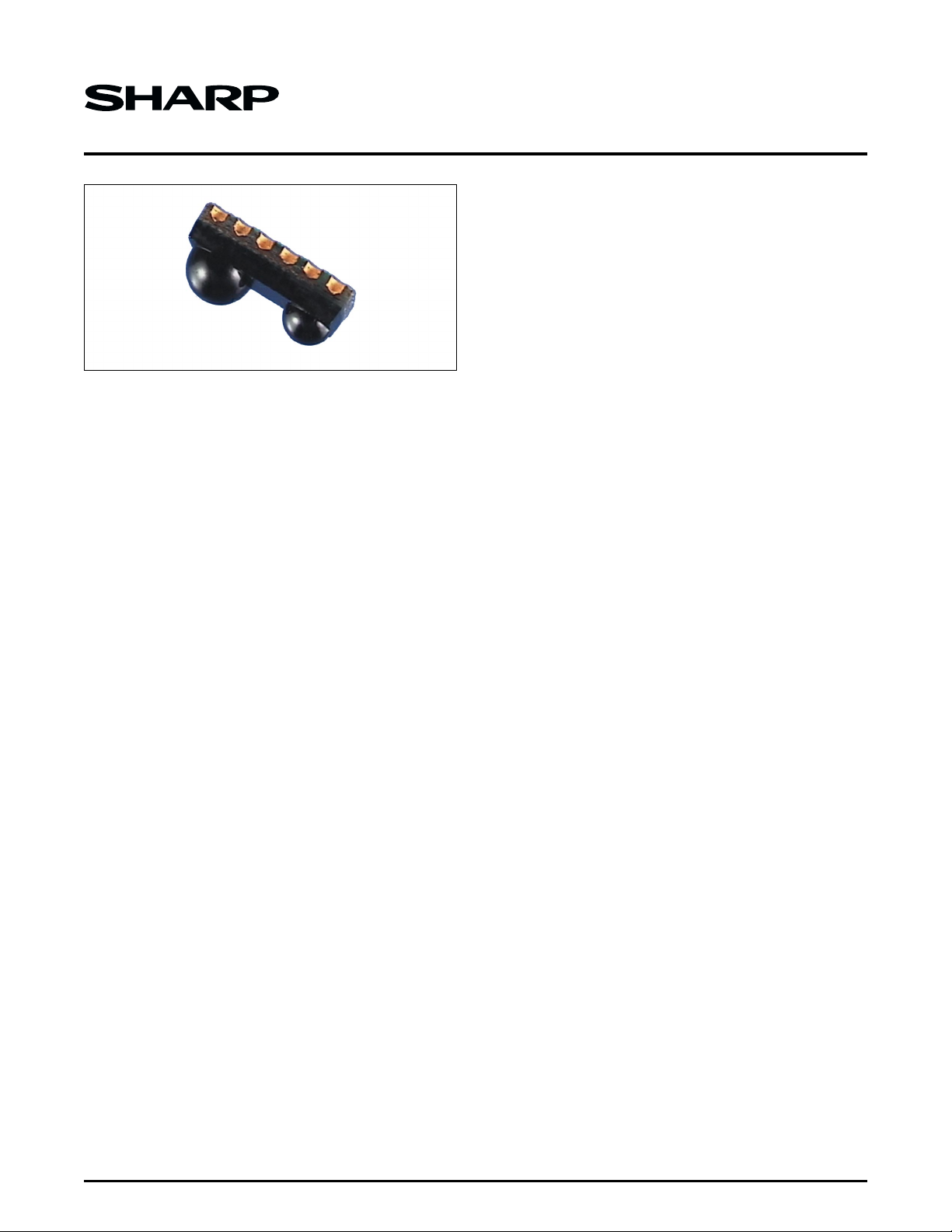
The SHARP GP2W0001YP is one of the smallest
transceiver modules. Even at low operating voltages,
it provides a reliable interface between logic and IR
signals for through-air, serial, half-duplex IR wireless
data links and is designed to satisfy IrDA physical
layer specifications.
Technical Information 1
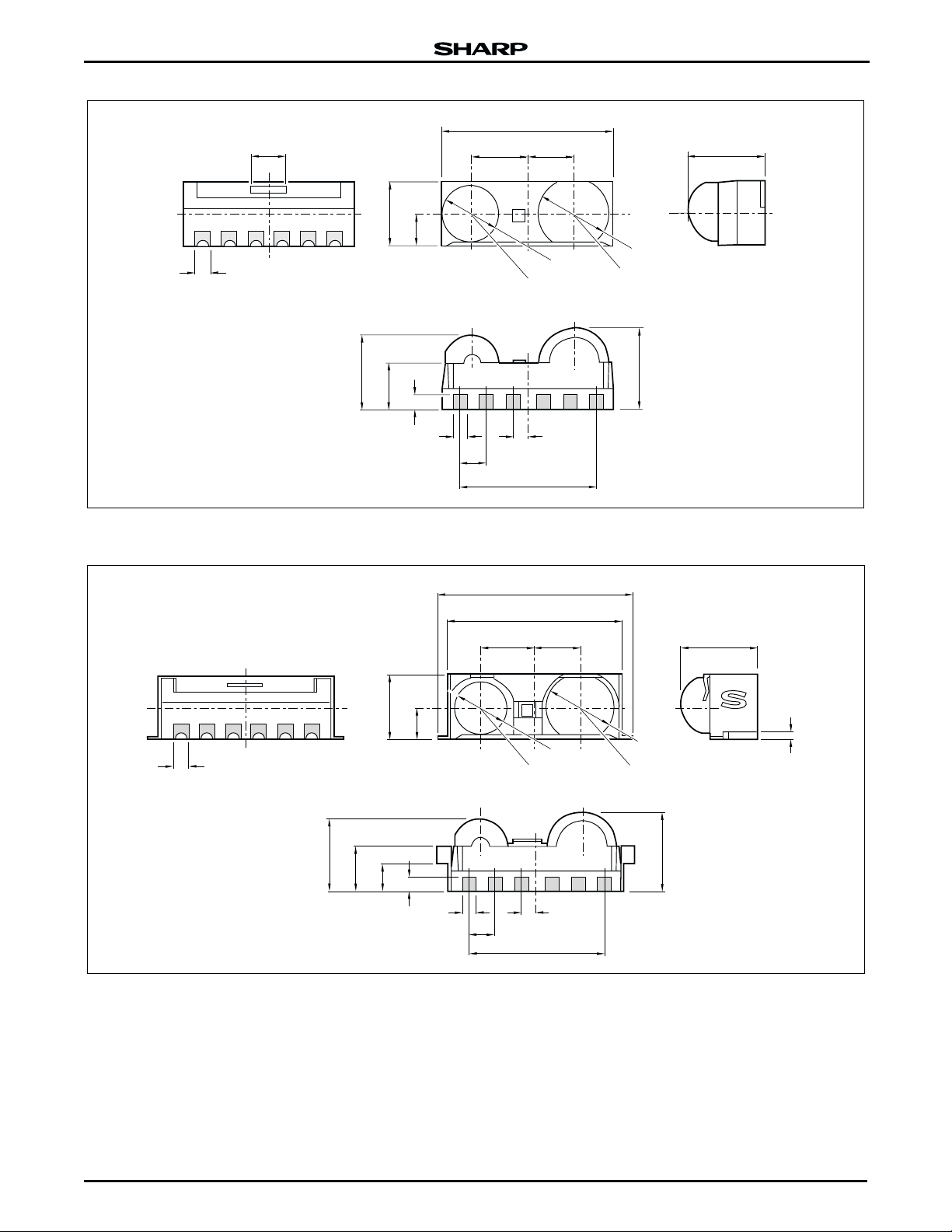
OUTLINE DIMENSIONS
The dimensions shown in Figure 1 and Figure 2 are
only for design reference, and are subject to change
without notice. The metal shield case version
GP2W0002YP, (for excellent noise immunity) is shown
in Figure 2. Contact your local SHARP office for the latest device specifications.
Page 2
GP2W0001YP/GP2W0002YP Low Power Infrared Transceiver
8.7
4.2
1.1
2.0
3.15
1.7
2.95
TRANSMITTER
CENTER
2.325
φ2.8
φ3.6
RECEIVER
CENTER
NOTES:
1. Dimensions are in mm.
2. Unspecified tolerances are ±0.3 mm.
3. Resin burrs are not included in this
outline dimension drawing.
4. Package material: Visible light
cut-off resin (Color: black)
5. Weight: Approximately 0.12 g
6. Pin assignment: See Figure 5 and Table 1.
Figure 1. GP2W0001YP Outline Dimensions
1.1
3.5
2.2
3.4
0.8
1.7
0.8
1.4
0.7
7.0
10.2
9.2
2.95
2.325
TRANSMITTER
CENTER
φ2.8
4.2
φ3.6
RECEIVER
CENTER
GP2W0001YP-20
4.2
0.7
NOTES:
1. Dimensions are in mm.
2. Unspecified tolerances are ±0.3 mm.
3. Resin burrs are not included in this
outline dimension drawing.
4. Package material: Visible light
cut-off resin (Color: black)
5. Weight: Approximately 0.12 g
6. Pin assignment: See Figure 5 and Table 1.
3.5
2.2
1.55
0.8
0.8
1.4
0.7
7.0
4.2
GP2W0001YP-21
Figure 2. GP2W0002YP (with Shielding Case) Outline Dimensions
2 Technical Information
Page 3
Low Power Infrared Transceiver GP2W0001YP/GP2W0002YP
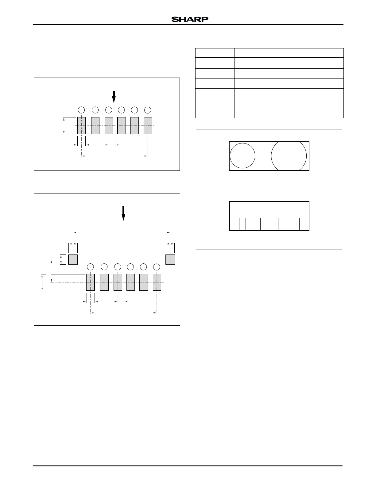
Solder Paste Footprints
Figure 3 and Figure 4 are the Solder Paste footprint
drawings for both parts. Note that the GP2W0002YP
footprint in Figure 4 is compatible with both parts.
LENS (PD/LED) SIDE
23456
1
1.7
0.9
P 1.4 × 5 = 7
NOTE: Viewed from the parts side of PCB.
Figure 3. GP2W0001YP Soldering Footprint
LENS (PD/LED) SIDE
0.7
GP2W0001YP-22
Table 1. Pinouts
PIN NO. DESCRIPTION SYMBOL
1 LED Anode LEDA
2 Transmitter Data Input TxD
3 Shut Down Circuit Input SD
4 Receiver Data Output RxD
5 Ground GND
6 Supply Voltage V
PIN 1 PIN 6
CC
10
0.8
1.05
2.025
1.7
0.9
P 1.4 × 5 = 7
NOTE: Viewed from the parts side of PCB.
23456
0.7
GP2W0001YP-23
Figure 4. GP2W0002YP Soldering Footprint
0.8
PIN 1 PIN 6
GP2W0001YP-28
Figure 5. Pin Locations
1
Technical Information 3
Page 4
GP2W0001YP/GP2W0002YP Low Power Infrared Transceiver
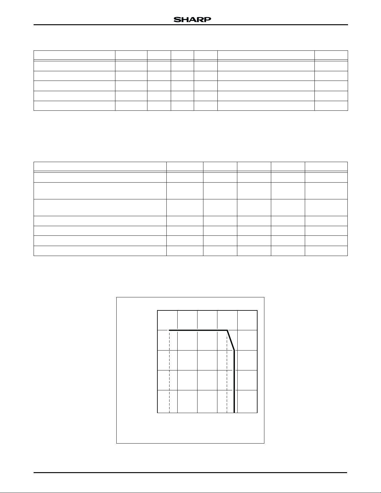
ABSOLUTE MAXIMUM RATINGS
PARAMETER SYMBOL MIN. MAX. UNIT CONDITIONS NOTE
Supply Voltage V
Peak Forward LED Current I
Operating Temperature T
Soldering Temperature T
Storage Temperature T
CC
FM
OPR
SOL
STG
06.0V
500 mA Pulse 78.1 ms, 3/16-duty cycle 1, 2, 3
-10 +70 °C3
230 °C Solder reflow time: 5 seconds
-20 +85 °C
NOTES:
1. An in-band optical signal is a pulse/sequence where the peak
wavelength,
pulse characteristics are compliant with the IrDA Physical Layer
λp, is defined as 850 nm < λp < 900 nm, and the
2. See ‘IrDA Physical Layer Link Specification, Appendix A’ for
ambient light conditions.
3. See Figure 6.
RECOMMENDED OPERATING CONDITIONS
PARAMETER SYMBOL MIN. MAX. UNIT NOTE
Supply Voltage V
Logic High Transmitter Input
Voltage (TxIN)
Logic Low Transmitter Input
Voltage (TxIN)
Shutdown Circuit High Level Input Voltage V
Shutdown Circuit Low Level Input Voltage V
V
IHTXD
V
ILTXD
CC
IHSD
ILSD
Data Rate BR 2.4 115.2 Kbps
Operating Temperature T
NOTES:
1. Measured at the input circuit, not the device pin. Tx input should
not exceed 0.8 V
2. 0.4 or Open
CC.
OPR
2.7 5.5 V
2.4 V
CC
0.4 V
VCC – 0.6 V
CC
0.0 0.4 V 2
-10 70 °C
V1
V
400
(mA)
300
200
100
0
-10 60 70
0
AMBIENT TEMPERATURE T
(°C)
A
GP2W0001YP-27
100755025
PEAK
FORWARD
CURRENT
I
FM
Figure 6. Peak Forward Current vs. Temperature
4 Technical Information
Page 5
Low Power Infrared Transceiver GP2W0001YP/GP2W0002YP
ELECTRICAL AND OPTICAL SPECIFICATIONS
PARAMETER SYMBOL MIN. TYP. MAX. UNIT CONDITIONS NOTES
Supply Voltage V
Maximum Reception
Distance
CC
L1 ≥ 0.2 m 2Θ
L2 ≥ 1.0 m 2Θ
2.7 5.5 V
Data Rate BR 2.4 115.2 Kbps
Operating Temperature T
OPR
-10 70 °C
RECEIVER
High Level Output Voltage
Low Level Output Voltage
V
OH
V
OH
V
OL1
V
OL2
4.5 V VCC = 5 V
2.5 V VCC = 3 V
0.6 V VCC = 5 V, IOL = 400 mA RxD = ON 3
0.6 V VCC = 3 V, IOL = 400 mA RxD = ON 3
Viewing Angle 2Θ 30 degrees
Low Level Pulse Width
t
t
W1
W2
0.8 16 µs BR = 2.4 Kbps (pulse width 78.12 µs)
0.8 8 µs BR = 115.2 Kb/s (pulse width 1.63 µs)
1.0 1.4 mA
I
CC1
Current Consumption 0.7 1.0 mA
1.0 µA Shut-down Mode
1.2 µs 3
0.2 µs 3
Rise Time t
Fall Time t
I
CC2
R
F
TRANSMITTER
Radiant Intensity
I
E1
I
E2
3.6 28.8 mW/sr IF = 27 mA, 2Θ
40 350 mW/sr IF = 300 mA, 2Θ
Peak Emission Wavelength λp 850 870 900 nm I
Peak LED Current I
LEDA
High Level Input Voltage V
Low Level Input Voltage V
IH
IL
500 mA
2.4 V
CC
0.0 0.4 V
V
≤ 15°, IE = 3.6 mW/sr
1/2
≤ 15°, IE = 40 mW/sr
1/2
No input signal, VCC = 5.0 V, output open,
= VCC - 0.6 V
V
IHSD
No input signal, V
V
= VCC - 0.6 V
IHSD
= 20 mA
F
= 3.0 V, output open,
CC
≤ 15°
1/2
≤ 15°
1/2
All modes, PW = 78.1 µs or less,
3/16 duty cycle
Measured at input circuit. Device pin will
usually not exceed 0.8 V
NOTES:
1. These specifications reflect the Recommended Operating Conditions, unless otherwise noted.
2. All typical values are at 25°C and 3.3 V, ambient light on the
receiver surface under 10 Lux, unless otherwise noted.
3. See Figure 7, Figure 8, and Figure 9
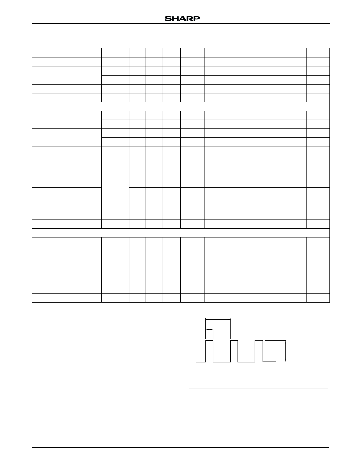
NOTE: At BR = 2.4 Kbps: t1 = 416.7 µs, t2 = 78.1 µs
At BR = 115.2 Kbps: t
t
1
t
2
RADIATION
INTENSITY OF
TRANSMITTER
3.6 mW/Sr MIN.
= 8.68 µs, t2 = 1.63 µs
1
GP2W0001YP-24
Figure 7. Detector Input Signal Waveform
Technical Information 5
Page 6

GP2W0001YP/GP2W0002YP Low Power Infrared Transceiver
t
R
V
OH
90%
t
F
50%
10%
t
W
V
OL
GP2W0001YP-7
Figure 8. Output Waveform Specification
= 3 V,
V
CC
= 2.2 Ω
R
L
= 1,500 pF
1.63 µs
Tx = 2.7 V
V
IN
CX
2
Tx TxD
= 1 kΩ
R
2
GP2W0001YP
BR = 115.2 Kbps
Figure 9. Recommended Emitter Circuit
GP2W0001YP-26
TRANSMITTER
(NOTE 1)
NOTES:
1. Transmitter uses GP2W0001YP (λp = 870 nm TYP.)
adjusted to a radiation intensity of 3.6 mW/Sr.
2. φ Indicates horizontal and vertical directions.
3. Ee: Detector face illuminance < 10 lx
Figure 10. Standard Optical Detector System
E
e
φ
φ
GP2W0001YP
OSCILLOSCOPE
L
GP2W0001YP-25
6 Technical Information
Page 7

Low Power Infrared Transceiver GP2W0001YP/GP2W0002YP
ELECTRICAL DESIGN APPLICATION TIPS
Figure 11 shows a circuit application and passive
component values for a GP2W0001YP. The values
shown are only for reference. Contact your local Sharp
office concerning technical reference data for optical/
electrical characteristics.
Circuit Application and
External Passive Components
The circuit application and the external passive com-
ponents shown in Figure 11 enable the GP2W0001YP
to operate at both one-meter and 20 cm low power
option communication modes at V
= 3.0 V.
CC
SHUTDOWN MODE
The ‘Shutdown’ pin is an active LOW terminal.
Shutdown mode only affects the power consumption
of the receiver circuits. The transmitter LED can still be
operated when SD is asserted. The two circuits are
independent and not internally connected. The transmitter circuit does not consume current unless a drive
signal is applied.
Table 2. SD Pin Functions
INPUT PERFORMANCE
HIGH Normal Mode
LOW Shutdown Mode
OPEN Shutdown Mode
6 54321
CX
1
R
R
1
V
CC
COMPONENTS
CX
1
CX
2
R
1
R
2
R
L
NOTE: All recommended values are for V
RxD TxDSD
RECOMMENDED VALUES
47 µF, 6.3 V or as appropriate
1,500 pF, 25 V
47 Ω, ±5%, 1/10 W
1 kΩ, ±5%, 1/10 W
2.2 Ω ±5%, 1/2 W,1 meter
33 Ω ±1%, 1/8 W, 20 cm
(low power)
2
Figure 11. External Components
CX
CC
2
= 3.0 V
R
L
GP2W0001YP-29
V
SD
RxD
OPERATABLE
40 ms
IH
V
IL
(or OPEN)
HIGH
LOW
GP2W0001YP-30
Figure 12. Receiver Activation
Technical Information 7
Page 8

GP2W0001YP/GP2W0002YP Low Power Infrared Transceiver
Signal Waveform Example
Figure 14 shows examples of each waveform when
operating a GP2W0001YP to IrDA standards. Note that
the IrDA bitstream is inverted in the encoder and
decoder circuits, and the output pulse is sent during a
‘0’ bit. The examples are for reference only, to help
understand the GP2W0001YP hardware, and device
signal measurements. The receiver output is not gated,
and will send output for the entire period of the received
IR input signal. Refer to Figure 14 for waveform reference points.
T
1
2
3
0
3/16T
T
10 1
3
2
4
ENCODER
CIRCUIT
DECODER
CIRCUIT
1
5
GP2W0001YP-31
Figure 13. GP2W0001YP Block Diagram
4
5
NOTES:
1 Transmit data waveform
2
Encoder circuit output waveform
3 Transmitter output optical signal waveform
4 GP2W0001YP receiver output waveform
5
Receive data waveform
T =
Data rate: 2.4 Kbps, 9.6 Kbps, 19.2 Kbps, 38.4 Kbps,
1
Data Rate
0
57.6 Kbps, 115.2 Kbps
10 1
Figure 14. Signal Waveform Example
GP2W0001YP-32
8 Technical Information
Page 9

Low Power Infrared Transceiver GP2W0001YP/GP2W0002YP
MECHANICAL DESIGN
APPLICATION TIPS
Recommended Footprint
Figure 15 shows the basic recommended footprint
for PCB design using the SHARP GP2W0001YP infrared transceiver module. All values shown here are for
reference, and are in mm.
1.5 1.1
2
0.75
6 - 0.9
P1.4
Electro-Mechanical Design Tip
Figure 16 gives a recommended set of locations for
resistors and capacitors for better performance, particularly for the power supply (V
shown in Figure 16, should be mounted near the
GP2W0001YP transceiver module for best performance. All values in Figure 16 are for reference and
are in mm.
1.1
1.5
) line. R1 and CX1, as
CC
6 - 2.6
NOTE: Dimensions are in mm.
7.0
GP2W0001YP-33
Figure 15. Recommended Footprint
Technical Information 9
Page 10

GP2W0001YP/GP2W0002YP Low Power Infrared Transceiver
2
0.75
1.5 1.1
6 - 0.9
P1.4
7.0
1.1
1.5
6 - 2.6
NOTE: Dimensions are in mm.
Capacitor and resistor on the power
trace should be located as close as
possible to the GP2W0001YP
transceiver module.
V
CC
GND
GP2W0001YP-34
Figure 16. PCB Design Tip
10 Technical Information
Page 11

Low Power Infrared Transceiver GP2W0001YP/GP2W0002YP
Cabinet and IR Cosmetic
Window Design Tips
Figure 17 with its calculations illustrates the design
tips for a cabinet and an IR cosmetic window with ±18°
viewing angles in the vertical and horizontal axes. All
transceiver dimension values are for reference, and
are in mm.
The optical window size should be the minimum size
of W × H, either rectangular or elliptical, to maintain
w
(8.475)
18
˚
W
18
˚
IrDA data transfer performance. The dimensions for W
can be calculated by the formula:
W = 2 × L × tan(18 + w)
And the dimensions for H can be calculated by the
formula:
H = 2 × L × tan(18 +h)
In the case where the viewing angle is +18°, which
conforms to or exceeds the IrDA Serial Infrared Physical Layer Link Specifications. Values to be calculated
with above the formula must be given in mm.
L
L
h
(3.15)
18
18
˚
H
˚
NOTE: Dimensions are in mm.
GP2W0001YP-35
Figure 17. Optical Window Tips
Technical Information 11
Page 12

GP2W0001YP/GP2W0002YP Low Power Infrared Transceiver
Evaluation Board
Figure 18 shows the recommended evaluation circuit for the GP2W0001YP/GP2W0002YP devices. This
circuit is provided on an evaluation board for test and
evaluation purposes. Samples are available through
your Sharp support office or Sales Representative.
The resistor value for RL is based on the supply voltage. For the one-meter range, the parallel combination
of the three values should be adjusted to approximately
Ω when V
2.2
300 mA with approximately 200 mW being dissipated in
the resistors. For the 20 cm (reduced) range, the value is
adjusted to 33
and the resistive power dissipation will be approximately
31 mW.
= 3.3 V, yielding a forward current of
CC
Ω, the nominal forward current is 27 mA,
When the 33
Ω value and a forward current of 27 mA
is used, a total of 31.3 mW is dissipated during LED ontime. This dissipation is within the rating of the SR1206
package. When used at a data rate of 115 Kbps, the
maximum on time is 18.75% of a bit time when the LED
is ‘ON.’ Since only the logical ‘0’ values of a data string
are sent, the overall duty cycle is below this value.
The board carries three positions to allow the use of
a combination of standard resistor values. To create
the 2.2
parallel. For the 43
used or three parallel resistors of 130
Ω value, three 6.6 Ω resistors are connected in
Ω value, one 43 Ω resistor can be
Ω. The resistor
positions on the board are in the SR1206 footprint,
which supports one-quarter Watt resistors.
This test and evaluation board is not intended for
production applications, and should not be subjected to
long periods at elevated temperature. Operation of the
board should be limited to free-air test conditions.
RL 2.2 Ω - 33 Ω
R
5
R
4
R
3
GND
V
CC
J1
+
+
+
+
+
2 × 5
+
+
+
+
+
2 V
CC
4 TxD
6 RxD
8
10
R
47 Ω
1
1
3
5
7
9
C2 1,500 pF 25 V
R
2
1K
Figure 18. GP2W0001YP Test Circuit
C
1
47 µF TANT
1
LEDA
2
TxD
3
SD
4
RxD
5
GND
6
V
CC
GP2W0001YP
GP2W0001YP-36
12 Technical Information
Page 13

Low Power Infrared Transceiver GP2W0001YP/GP2W0002YP
MOISTURE-PROOF PACKING
INFORMATION
Scope
This section describes the specifications of
GP2W0001YP/GP2W0002YP moisture-proof packing,
and is only for reference. The official specifications
should be consulted for packing information.
Packing Material Specifications
The GP2W0001YP/GP2W0002YP reel is moistureproof packed for shipment. Table 3 describes the materials used for each item of the moisture-proof packing.
Packing Method
1. Seal the aluminum laminate bag that contains the
tape reel (2,000 devices/reel) and desiccant.
2. Fill in the necessary information on the label and
paste it on the aluminum laminate bag.
3. Pack 4 aluminum laminated bags (1 reel each) into
the designated outer case, placing paper pads on
the bottom and top of the outer case, as well as be-
tween each layer of the aluminum laminated bags.
See Table 4.
4. Seal the outer case with craft tape, indicating the
model name, quantity, and out-going inspection date
on the case. (8,000 pieces total per carton)
TREATMENT AFTER UNSEALING
1. After unsealing, devices should be mounted at a
temperature of 10°C to 30°C, humidity below 60%
RH, within 3 days.
2. For long term storage, devices should either be
stored in a dry box, or re-sealed in a moisture-proof
bag with desiccant and stored in an environment
where the temperature is 10°C to 30°C, humidity below 60% RH. Devices must be mounted within 2
weeks.
BAKING BEFORE MOUNTING
If the devices are not kept in the storage conditions
described above, or the desiccant indicator has turned
pink, baking must be performed before devices are
mounted: baking may only be done once.
• Recommended Baking Conditions: 100°C
12 to 24 hours
NOTE: Do not bake the devices while they are still on the reel — the
reel will melt. Parts should be either temporarily mounted to
a PCB with adhesive, or placed in a metal tray. Any device
that has been out of its dry pack for more than 72 hours
should be dried in some manner prior to any automated surface mount reflow process. Otherwise these devices should
be mounted and soldered by hand.
Table 3. Packing Materials
Storage and Treatment
ITEM MATERIAL
Aluminum Laminate Bag Aluminum Polyethylene
STORAGE CONDITIONS
The product should be stored under these conditions:
• Storage temperature: 10°C to 30°C
• Humidity: below 60% RH
Label Paper
Desiccant
Outer Case Paper
Pads Paper
Table 4. Packing Quantities
PACKING SHAPE PRODUCT QUANTITY PER REEL QUANTITY PER BAG
Tape reel (
NOTE: Minimum order/shipment quantity should be one laminated bag (1 reel of 2,000 pieces).
∅ 330 mm) 1 model 2,000 pieces 1 reel
Technical Information 13
Page 14

GP2W0001YP/GP2W0002YP Low Power Infrared Transceiver
LIFE SUPPORT POLICY
SHARP components should not be used in medical devices with life support functions or in safety equipment (or similiar applications where
component failure would result in loss of life or physical harm) without the written approval of an officer of the SHARP Corporation.
LIMITED WARRANTY
SHARP warrants to its Customer that the Products will be free from defects in material and workmanship under normal use and service for a
period of one year from the date of invoice. Customer's exclusive remedy for breach of this warranty is that SHARP will either (i) repair or
replace, at its option, any Product which fails during the warranty period because of such defect (if Customer promptly reported the failure to
SHARP in writing) or, (ii) if SHARP is unable to repair or replace, refund the purchase price of the Product upon its return to SHARP. This
warranty does not apply to any Product which has been subjected to misuse, abnormal service or handling, or which has been altered or
modified in design or construction, or which has been serviced or repaired by anyone other than Sharp. The warranties set forth herein are in
lieu of, and exclusive of, all other warranties, express or implied. ALL EXPRESS AND IMPLIED WARRANTIES, INCLUDING THE
WARRANTIES OF MERCHANTABILITY, FITNESS FOR USE AND FITNESS FOR A PARTICULAR PURPOSE, ARE SPECIFICALLY
EXCLUDED. In no event will Sharp be liable, or in any way responsible, for any incidental or consequential economic or property damage.
The above warranty is also extended to Customers of Sharp authorized distributors with the following exception: reports of failures of Products
during the warranty period and return of Products that were purchased from an authorized distributor must be made through the distributor.
In case Sharp is unable to repair or replace such Products, refunds will be issued to the distributor in the amount of distributor cost.
SHARP reserves the right to make changes in specifications at any time and without notice. SHARP does not assume any responsibility
for the use of any circuitry described; no circuit patent licenses are implied.
NORTH AMERICA
SHARP Microelectronics
of the Americas
5700 NW Pacific Rim Blvd.
Camas, WA 98607, U.S.A.
Phone: (360) 834-2500
Telex: 49608472 (SHARPCAM)
Facsimile: (360) 834-8903
EUROPE
SHARP Electronics (Europe) GmbH
Microelectronics Division
Sonninstraße 3
20097 Hamburg, Germany
Phone: (49) 40 2376-2286
Facsimile: (49) 40 2376-2232
http://www.sharpmed.com
ASIA
SHARP Corporation
Integrated Circuits Group
2613-1 Ichinomoto-Cho
Tenri-City, Nara, 632, Japan
Phone: +81-743-65-1321
Facsimile: +81-743-65-1532
http://www.sharp.co.jp
http://www.sharpsma.com
©2000 by SHARP Corporation Reference Code SMA00060
 Loading...