

Page 1
Compact, Thin Type
GP2L23L/GP2L23R
Photointerrupter
GP2L23L/GP2L23R
■ Features
1. Correspond to prism system
2. Compact and thin (Thickness: 3mm
)
■ Applications
1. Specified for tape-end detection for digital
audio tape recorders
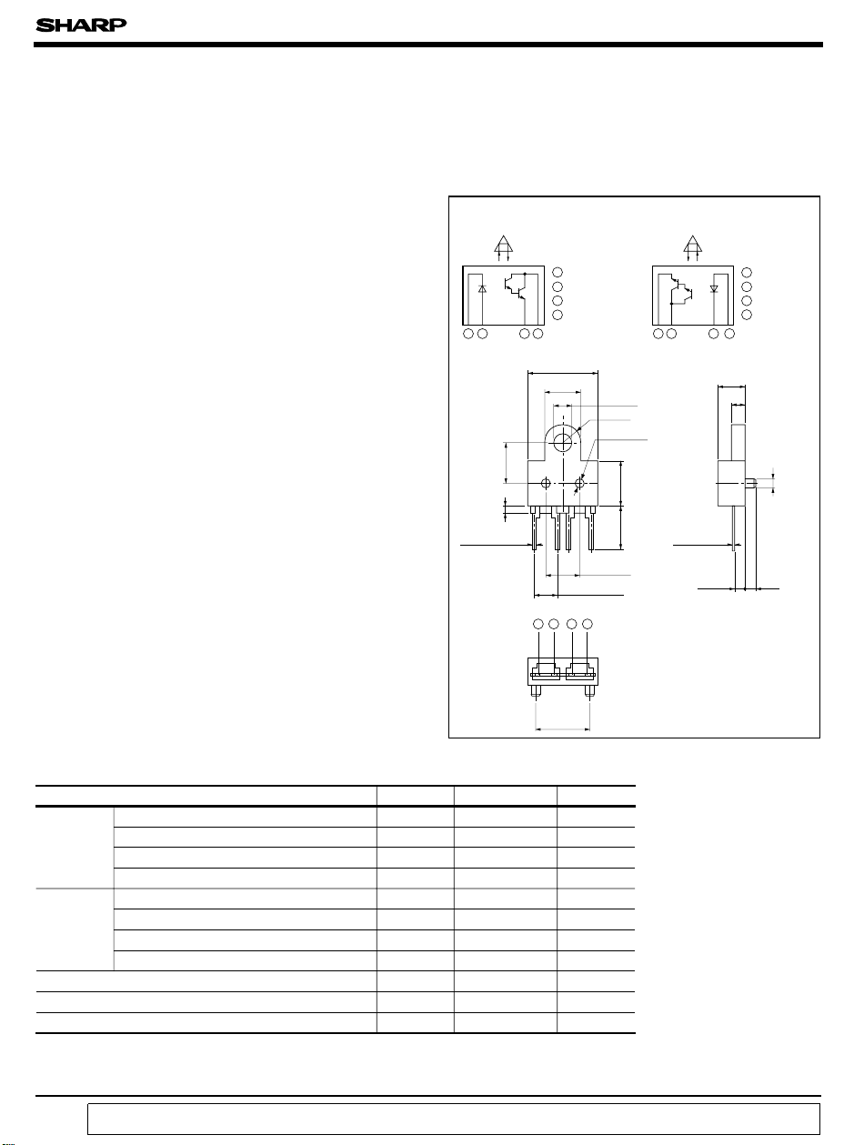
■ Outline Dimensions
Internal connection diagram
GP2L23L
1 Cathode
2 Anode
3 Emitter
4 Collector
4.5
MAX.
Resin burr
0.8
+ 0.3
- 0.1
41
7.75
4.0
2 -(2.54
12 34
3.75
φ
2.0
R2.0
2 -φ1.2
±
0.1
)
23
4- 0.45
(
Unit : mm
GP2L23R
1 Emitter
2 Collector
3 Cathode
4 Anode
12 34
3.0
1.5
∗∗
+ 0.3
- 0.1
(
1.15
L
)
5.0
)
5.0
0.25
(
∗ Tolerance:±0.15mm
∗ ( ): Reference dimensions
∗∗ L : GP2L23L
R: GP2L23R
1.0
1.0
φ
2 -
)
±0.1
6.0
■ Absolute Maximum Ratings
(
Ta= 25˚C
)
Parameter Symbol Rating Unit
Forward current
∗1
Input
Peak forward current
Reverse voltage
Power dissipation
Collector-emitter voltage
Output
Emitter-collector voltage
Collector current
Collector power dissipation
Operating temperature
Storage temperature
∗2
Soldering temperature
∗1 Pulse width<=100 µs, Duty ratio= 0.01
∗2 For 3 seconds
“ In the absence of confirmation by device specification sheets, SHARP takes no responsibility for any defects that occur in equipment using any of SHARP's devices, shown in catalogs,
data books, etc. Contact SHARP in order to obtain the latest version of the device specification sheets before using any SHARP's device.”
I
F
I
FM
V
R
P75mW
V
CEO
V
ECO
I
C
P
C
T
opr
T
stg
T
sol
50 mA
1A
6V
35 V
6V
40 mA
75 mW
- 20 to + 85 ˚C
- 40 to + 100 ˚C
260 ˚C
Page 2
GP2L23L/GP2L23R
■ Electro-optical Characteristics
Parameter Symbol Conditions MIN. TYP. MAX. Unit
I
Input
Forward voltage V
Peak forward voltage V
Output Reverse current
Collector dark current
∗3
Transfer
characteristics
Collector current
Response time
∗4
Leak current
Rise time
Fall time
I
I
I
CEO
I
LEAK
F
FM
R
C
t
r
t
f
∗3 The condition and arrangement of the reflective object are shown in the following drawing
∗4 Without reflective object
Test Condition and Arrangement
for Collector Current
MONOSASHI
PRISM
13mm
GP2L23L
GP2L23R
= 20mA
F
= 0.5A
I
FM
=3V
V
R
= 10V
V
CE
= 5V, IF= 20mA
V
CE
= 2V, IC= 10mA
V
CE
= 100Ω, d= 13mm
R
L
= 5V, IF= 20mA
V
CE
(
Ta=25˚C
)
- 1.2 1.4 V
-34V
--10µA
--10-6A
0.8 - 15 mA
- 80 400
- 70 350
µ s
µ s
--50µA
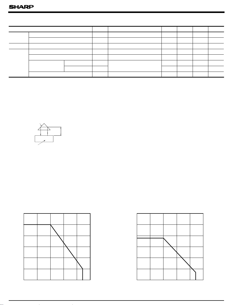
Fig. 1 Forward Current vs.
Ambient Temperature
60
50
)
mA
40
(
F
30
20
Forward current I
10
0
- 25 0 25 50 75 85 100
Ambient temperature T
a
(˚C
Fig. 2 Collector Power Dissipation vs.
Ambient Temperature
120
)
100
mW
(
C
80
75
60
40
20
Collector power dissipation P
0
)
- 25 0 25 50 75 85 100
Ambient temperature Ta (˚C
)
Page 3
GP2L23L/GP2L23R
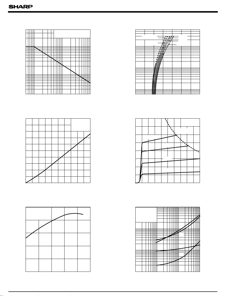
Fig. 3 Peak Forward Current vs.
Duty Ratio
Pulse width <= 100µ s
= 25˚C
T
a
)
mA
(
2000
1000
M
F
500
200
100
Peak forward current I
50
20
-2
55252
10
-1
10
Duty ratio
Fig. 5 Collector Current vs.
Forward Current
)
(
mA
C
20
18
16
14
12
V
T
a
CE
= 25˚C
10
8
6
Collector current I
4
2
100200
Forward current IF (mA
)
Fig. 7 Relative Collector Current vs.
Ambient Temperature
125
100
)
%
(
= 20mA
I
F
V
=5V
CE
75
=5V
Fig. 4 Forward Current vs.
Forward Voltage
500
)
mA
(
= 75˚C
T
200
100
100
F
a
50˚C
50
-
25˚C
0˚C
20˚C
20
5
Forward current I
2
1
1
0 0.5 1.0 1.5 2.0
Forward Voltage VF (V
2.5 3.0
)
3.5
Fig. 6 Collector Current vs.
Collector-emitter Voltage
)
mA
(
16
14
12
IF= 40mA
10
C
30mA
P
C(MAX.
T
= 25˚C
a
)
8
6
Collector current I
4
20mA
10mA
2
504030
0
02
13579
46810
Collector-emitter voltage VCE (V
)
Fig. 8 Response Time vs.
Load Resistance
1000
V
=2V
CE
500
= 10mA
I
C
= 25˚C
T
a
200
)
100
µ s
(
50
t
r
t
f
50
Relative collector curent
25
0
Ambient temperature Ta (˚C
20
10
Response time
5
t
d
t
s
2
111111111
1
)
5 10 20 100 200 1000
21-25 250 50 75 100
Load resistance RL (Ω
50 500
)
Page 4
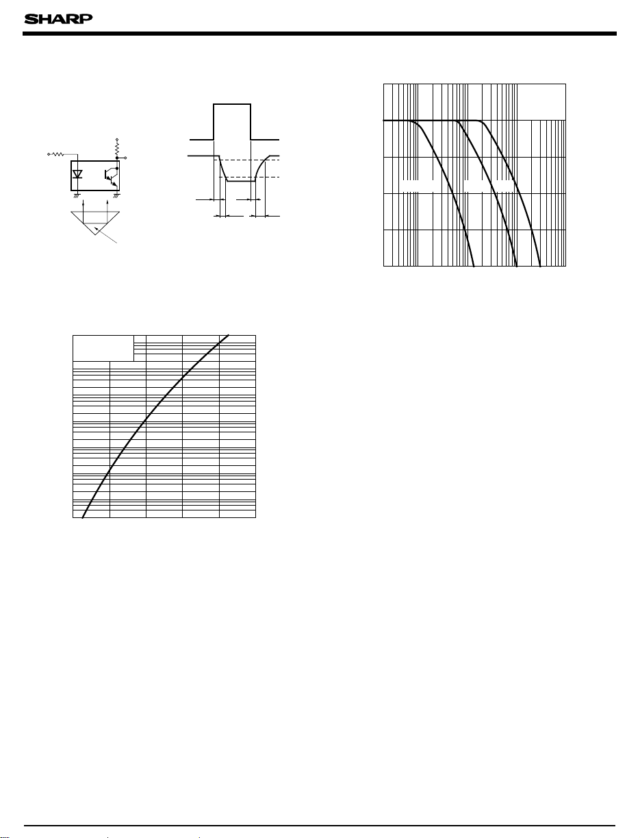
Test Circuit for Response Time
Input
V
R
D
CC
R
L
Output
MONOSASHI
PRISM
Input
Output
t
d
Fig.10 Collector Dark Current vs.
Ambient Temperature
-4
10
5
VCE= 10V
-5
10
)
5
A
(
-6
10
5
CEO
-7
10
5
-8
10
5
-9
10
5
Collector dark current I
-10
10
5
-11
10
- 25 0 25 50 75 100
Ambient temperature Ta (˚C
GP2L23L/GP2L23R
Fig. 9 Frequency Response
=2V
V
CE
I
= 10mA
C
T
= 25˚C
0
)
dB
(
-5
10%
90%
t
s
t
t
r
f
V
-10
Voltage gain A
R
=1kΩ
L
-15
-20
3
2 252525
5
10
4
10
Frequency f (Hz
)
a
10Ω100Ω
5
10
6
10
)
●
Please refer to the chapter “ Precautions for Use” .
 Loading...