

Page 1
GP2L22
GP2L22
Subminiature, High Sensitivity
Photointerrupter
■ Features
1. φ 4mm compact resin mold type
2. High sensitivity (IC: MIN. 0.5mA at IF= 4mA
3. Optimum detection distance: 0.6mm
4. Visible light cut-off type
■ Applications
1. Audio equipment, VCRs
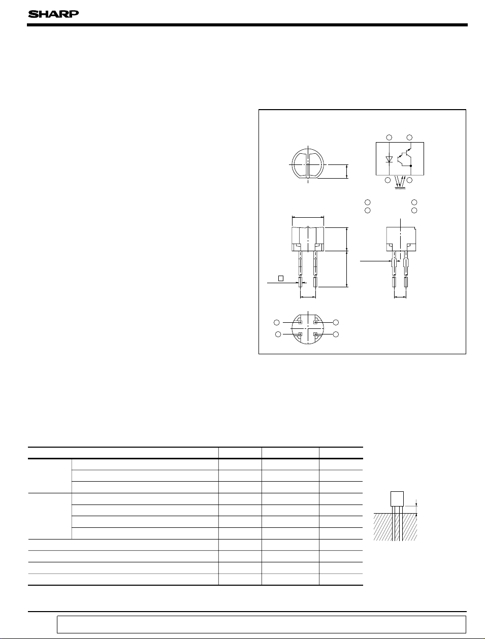
■ Outline Dimensions
Internal connection
)
φ 4.0
4-0.4
❈1.9
23
1
4
diagram
1.7
1 Anode
2 Cathode
3.0
)
4 -(0.6
1.0
±
13.5
∗Tolerance:±0.2mm
∗( ): Reference dimensions
∗
The dimensions indicated by ❈ refer
to those measured from the lead base.
(
Unit : mm
14
32
3 Collector
4 Emitter
❈1.5
)
■ Absolute Maximum Ratings
(
Ta= 25˚C
)
Parameter Symbol Rating Unit
Input
Forward current I
Reverse voltage V
F
R
50 mA
6V
Power dissipation P 75 mW
Collector-emitter voltage V
Output
Emitter-collector voltage V
Collector current I
Collector power dissipation P
Total power dissipation P
Operating temperature T
Storage temperature T
∗1
Soldering temperature T
∗1 For 3 seconds by manual soldering
“ In the absence of confirmation by device specification sheets, SHARP takes no responsibility for any defects that occur in equipment using any of SHARP's devices, shown in catalogs,
data books, etc. Contact SHARP in order to obtain the latest version of the device specification sheets before using any SHARP's device.”
CEO
ECO
C
C
tot
opr
stg
sol
35 V
6V
50
mA
75 mW
100 mW
- 25 to + 85
- 40 to + 100
˚C
˚C
260 ˚C
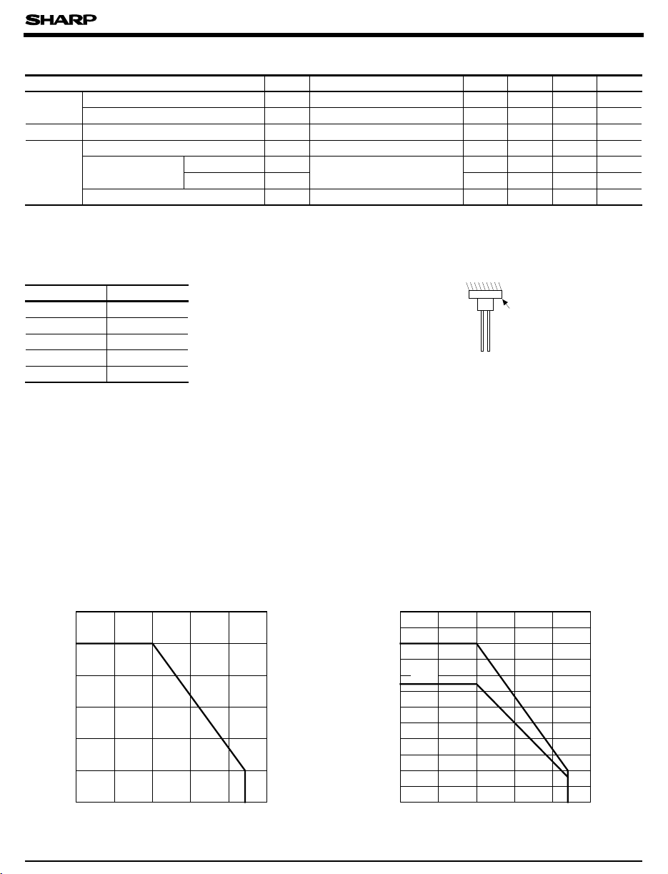
2mm or more
Soldering Area
Page 2
GP2L22
■ Electro-optical Characteristics
Parameter Symbol Conditions MIN. TYP. MAX. Unit
Input
Output
Transfer
characteristics
Forward voltage V
Reverse current I
Collector dark current I
∗2
Collector current I
Response time
∗3
Leak current I
Rise time
Fall time
R
CEO
C
t
t
LEAK
F
r
f
∗2 The condition and arrangement of the reflective object are shown in the right drawing.
∗3 Without reflective object
The ranking of collector current shall
be classified into the following 5 ranks.
Rank I
A 4.0 to 15.0
B 1.45 to 5.4
A or B 1.45 to 15.0
B or C 0.5 to 5.4
A, B or C 0.5 to 15.0
(mA
C
)
IF= 20mA - 1.2 1.4 V
VR=6V - - 10 µA
VCE= 10V - - 10
VCE= 5V, IF= 4mA 0.5 - 15 mA
V
= 2V, IC= 10mA
CE
RL= 100 Ω , d = 1mm
VCE= 5V, IF= 4mA - - 5 µA
Test Condition and
Arrangement for
Collector Current
- 80 400
- 70 400
Al evaporation
d = 1mm-thick glass
(
Ta= 25˚C
-6
)
A
µ s
µ s
Fig. 1 Forward Current vs.
Ambient Temperature
60
50
)
mA
40
(
F
30
20
Forward current I
10
0
- 25 0 25 50 75 85 100
Ambient temperature Ta (˚C
Fig. 2 Power Dissipation vs.
Ambient Temperature
120
P
tot
100
)
P,P
80
mW
(
60
40
Power dissipation P
20
)
c
0
025-25
Ambient temperature Ta (˚C
50 10075
85
)
Page 3

GP2L22
Fig. 3 Forward Current vs.
Forward Voltage
500
Ta= 75˚C
50˚C
)
mA
(
200
100
50
F
20
10
5
Forward current I
2
1
0
0.5 1 1.5 2 2.5 3 3.5
Forward voltage V
Fig. 5 Collector Current vs.
Collector-emitter Voltage
20
IF= 15mA
P
)
mA
(
C
10mA
10
7mA
C(MAX.
Fig. 4 Collector Current vs.
Forward Current
25˚C
0˚C
-
25˚C
)
mA
(
C
25
20
15
V
T
=5V
CE
= 25˚C
a
10
Collector current I
5
0
2.5 5.0 7.5 10.0 15.00
)
(V
F
Forward current I
(mA
F
12.5
)
Fig. 6 Collector Current vs.
Ambient Temperature
)
mA
(
C
5
I
= 4mA
F
V
=5V
4
CE
3
2
= 25˚C
T
a
)
Collector current I
4mA
2mA
0
2468100
Collector-emitter voltage VCE (V
Fig. 7 Collector Dark Current vs.
Ambient Temperature
-4
10
V
CE
5
= 10V
-5
10
5
)
A
-6
10
(
5
CEO
-7
10
5
-8
10
5
-9
10
5
-10
10
Collector dark current I
5
-11
10
5
-25 0
25 10050 75
Ambient temperature Ta (˚C
Collector current I
1
12
)
0
025-25
50 10075
Ambient temperature Ta (˚C
)
Fig. 8 Response Time vs.
Load Resistance
1000
100
)
µs
(
10
Response time
1
0.1
1
)
t
f
t
r
t
d
t
s
Load resistance R
L
(Ω
VCE=2V
I
= 10mA
C
T
a
100010010
)
= 25˚C
10000
Page 4

Test Circuit for Response time
Fig.9 Relative Collector Current vs.
Distance between Sensor and
Test Card
100
IF= 4mA
)
80
%
(
V
Ta= 25˚C
CE
GP2L22
=5V
V
CC
Input R
R
D
L
Output
Input
Output
Fig.10 Relative Collector Current vs.
Card Moving Distance
100
80
)
%
(
60
40
Relative collector current
20
0
-3 -2 -1 0 1 2 3
Card moving distance L(mm)
d= 1mm
I
F
V
T
t
d
= 4mA
=5V
CE
= 25˚C
a
60
40
10%
90%
t
s
t
t
r
f
Relative collector current
20
0
012 45
Distance between GP2L22 and test card d (mm
3
)
Test Condition for Distance & Detecting
Position Characteristics
Correspond to Fig.9
SHARP OMS TEST CARD
Correspond to Fig.10
SHARP OMS TEST CARD
d
(
White
GP2L22
)
GP2L22
WhiteBlack
0
Card moving direction
(
Distance = L
d
+-
)
■ Precautions for Use
(1)
Perform soldering manually.
(2)
Please refrain from soldering under preheating and refrain from soldering by reflow.
(3)
As for other general cautions, refer to the chapter “Precautions for Use” .
 Loading...