

Page 1
GP1A20
GP1A20
OPIC Photointerrupter with Cover
Case
■ Features
1. With cover case
2. High sensing accuracy (Slit width : 0.5mm
3. Operating supply voltage V
: 4.5 to 17V
CC
4. PWB mounting type package
■ Applications
1. Printers
2. Ticket vending machines
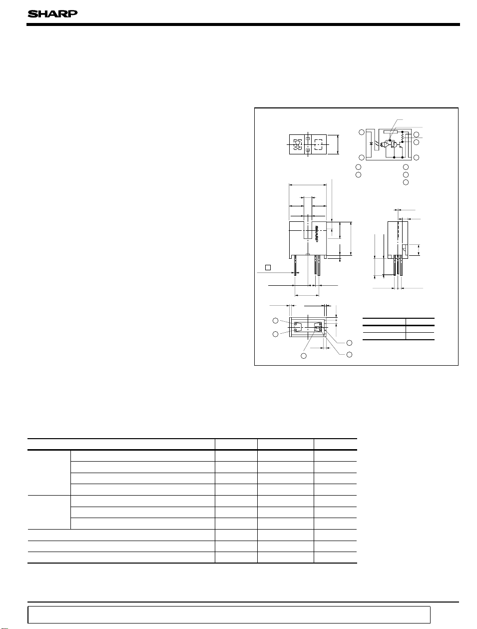
■ Outline Dimensions
Internal connection diagram
)
0.5
15.6
+
0.3
3.0
-
0
6.15 6.45
1.65 1.35
GP1A20
+ 0.3
5-0.45
-
0.1
(
10.6
(
1.5
)
(
)
0.75
1.0
4
(
5.445
(
0.75
2
1
)
)
1
8.0
23
1 Anode
2 Cathode
center
Detector
)
3.6
(
13.9
MIN.
1.6 7.5
8.0
)
(
1.27
* Unspecified tolerances shall be as follows;
Dimensions(d)Tolerance
1.0 1.6
6.0< d<=16.0 ±0.2
3
* ( ): Reference dimensions
5
(
Unit : mm
Voltage regulator
Amp.
5
10kΩ
4
3 V
CC
4 V
O
5 GND
Slit width
(
Both side of emitter and detector
0.5
2.5
MIN.
7.0
)
(
)
1.27
d<=6.0 ± 0.15
)
)
4.0
*“ OPIC” (Optical IC) is a trademark of the SHARP Corporation.
An OPIC consists of a light-detecting element and signal processing circuit integrated onto a single chip.
■ Absolute Maximum Ratings
(
Ta= 25˚C
)
Parameter Symbol Rating Unit
Input
Forward current I
*1
Peak forward current I
Reverse voltage V
F
FM
R
50 mA
1A
6V
Power dissipation P 75 mW
Output
Output current I
Power dissipation P
Operating temperature T
Storage temperature T
*2
Soldering temperature T
*1 Pulse width <=100µ s, Duty ratio= 0.01
*2 For 5 seconds
“ In the absence of confirmation by device specification sheets, SHARP takes no responsibility for any defects that occur in equipment using any of SHARP's devices, shown in catalogs,
data books, etc. Contact SHARP in order to obtain the latest version of the device specification sheets before using any SHARP's device.”
Supply voltage V
- 0.5 to + 17 V
CC
O
O
opr
stg
sol
- 25 to + 85 ˚C
- 40 to + 100 ˚C
50 mA
250 mW
260 ˚C
Page 2
GP1A20
■ Erectro-optical Characteristics
Parameter Symbol Conditions MIN. TYP. MAX. Unit
Input
Forward voltage V
Reverse current I
Operating supply voltage V
Low level output voltage V
Output
High level output voltage V
Low level supply current I
High level supply current I
“ Low→High” threshold input current*3I
*4
Transfer
characteristics
*3 I
FLH
*4 I
FHL
Hysteresis stands for I
Hysteresis
“ Low→High” propagation delay time
“ High→Low” propagation delay time
Response
time
represents forward current when output changes from low to high.
represents forward current when output changes from high to low.
FHL/IFLH
.
I
FHL/IFLHVCC
t
t
■ Recommended Operating Conditions
Parameter Symbol Operating temperature MIN. MAX. Unit
Low level output current I
Forward current I
OL
F
= 10mA - 1.1 1.4 V
FIF
VR=3V - - 10 µA
R
CC
OLIOL
OHVCC
CCLVCC
CCHVCC
FLHVCC
= 16mA, VCC= 5V, IF= 0 - 0.15 0.4 V
= 5V, IF= 10mA 4.9 - - V
= 5V, IF= 0 - 2.5 5.0 mA
= 5V, IF= 10mA - 1.0 3.0 mA
= 5V - 2.0 9.5 mA
4.5 - 17 V
= 5V 0.55 0.75 0.95
PLH
VCC=5V
PHL
= 10mA
I
F
r
= 280Ω
R
L
f
Ta= 0 to + 70˚C
-
-
- 0.1 0.5Rise time t
- 0.05 0.5Fall time t
-16mA
10 20 mA
39
515
(
Ta= 25˚C
)
-
µs
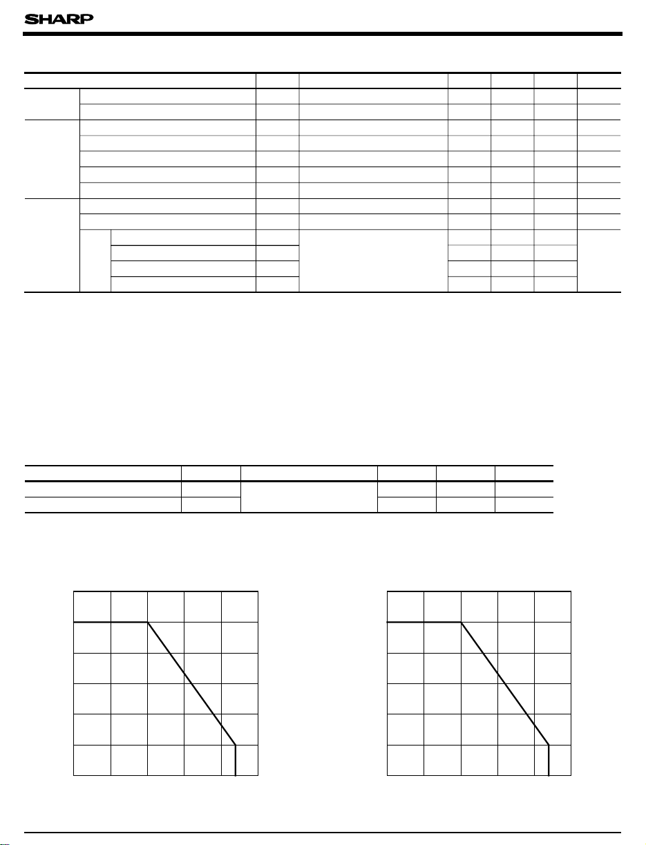
Fig. 1 Forward Current vs. Ambient
Temperature
60
50
)
mA
40
(
F
30
20
Forward current I
10
0
0
Ambient temperature Ta (˚C
)
Fig. 2 Output Power Dissipation vs.
Ambient Temperature
300
)
250
mW
(
O
200
150
100
50
Output power dissipation P
100755025
85-25 -25 85
0
0
25 50 75 100
Ambient temperature Ta (˚C
)
Page 3

GP1A20
Fig. 3 Low Level Output Current vs.
Ambient Temperature
60
)
50
mA
(
OL
40
30
20
Low level output current I
10
0
-25 85
0
25 50 75 100
Ambient temperature Ta (˚C
)
Fig. 5 Relative Threshold Input Current vs.
Supply Voltage
1.2
Ta= 25˚C
FLH
1.0
/I
FHL
0.8
0.6
I
FLH
I
FHL
Fig. 4 Forward Current vs. Forward Voltage
500
25˚C
0˚C
- 25˚C
)
mA
(
F
200
100
Ta = 75˚C
50˚C
50
20
10
5
Forward current I
2
1
Forward voltage VF (V
3.50 0.5 1 1.5 2 2.5 3
)
Fig. 6 Relative Threshold Input Current vs.
Ambient Temperature
1.4
V
=5V
CC
FLH
1.2
/I
I
FHL
1.0
0.8
I
FLH
I
FHL
0.4
Relative threshold input current I
0.2
0
5
= 1 at VCC=5V
I
FLH
Supply voltage V
)
(V
CC
Fig. 7 Low Level Output Voltage vs.
Low Level Output Current
1
0.5
)
V
(
OL
0.2
0.1
0.05
Low level output voltage V
0.02
0.01
Low level output current I
V
CC
= 25˚C
T
a
(mA
OL
=5V
502052
)
0.6
Relative threshold input current
0.4
201510
-25
I
= 1 at Ta= 25˚C
FLH
0
Ambient temperature Ta (˚C
100755025
)
Fig. 8 Low Level Output Voltage vs.
Ambient Temperature
0.4
V
=5V
)
V
0.3
(
OL
I
OL
0.2
0.1
Low level output voltage V
100101
0
-25
0
25 50 75 100
Ambient temperature Ta (˚C
CC
= 30mA
16mA
5mA
)
Page 4

GP1A20
Fig. 9 Supply Current vs. Supply Voltage
6
5
)
mA
(
4
3
CCL
I
CCL
2
Supply current I /ICCH
1
I
CCH
0
414
268101216
Supply voltage VCC (V
=-
T
a
Ta=- 25˚C
)
25˚C
25˚C
85˚C
25˚C
85˚C
Fig.11 Rise Time, Fall Time vs. Load Resistance
0.5
)
0.4
µs
(
f
, t
r
0.3
0.2
t
V
I
F
T
r
=5V
CC
= 10mA
= 25˚C
a
Fig.10 Propagation Delay Time vs.
Forward Current
7
)
6
µs
(
PHL
5
, t
PLH
4
3
2
1
Propagation delay time t
0
0
10
Forward current I
20 30
(mA
F
VCC=5V
R
L
T
a
)
t
PHL
t
PLH
= 280 Ω
= 25˚C
40 50
Rise time, fall time t
0.1
0
Load resistance R
L
t
f
(kΩ
520.5
1010.2
)
Test Circuit for Response Time
Input
Output
50%
t
PLH
t
PHL
t
r
t
90%
10%
f
V
OH
1.5V
V
OL
= tf= 0.01 µ s
t
r
ZO= 50Ω
Voltage regulator
(
V
IN
10kΩ
Amp.
47Ω
+ 5V
280Ω
)
VO
0.01µF
GND
■ Precautions for Use
(1) In this product, flux in the cleaning solvent may remain inside the slit of holder.
It sometimes causes lower output;therefore, cleaning is prrhibited.
(1) In order to stabilize power supply line, connect a by-pass capacitor of more than 0.01µF
between Vcc and GND near the device.
(3) As for other general cautions< refer to the chapter “Precautions for Use”.
 Loading...