

Datasheet GMS87C1408SK, GMS87C1408D, GMS87C1408, GMS87C1404SK, GMS87C1404D Datasheet (HYNIX)
...Page 1

June. 2001 Ver 1.2
8-BIT SINGLE-CHIP MICROCONTROLLERS
GMS81C1404
GMS81C1408
User’s Manual
Page 2

Table of Contents
OVERVIEW . . . . . . . . . . . . . . . . . . . . . . . 1
Description . . . . . . . . . . . . . . . . . . . . . . 1
Features . . . . . . . . . . . . . . . . . . . . . . . . 1
Development Tools . . . . . . . . . . . . . . . . 2
Ordering Information . . . . . . . . . . . . . . . 2
BLOCK DIAGRAM . . . . . . . . . . . . . . . . . 3
PIN ASSIGNMENT . . . . . . . . . . . . . . . . . 4
PACKAGE DIAGRAM . . . . . . . . . . . . . . . 5
PIN FUNCTION . . . . . . . . . . . . . . . . . . . . 6
PORT STRUCTURES . . . . . . . . . . . . . . . 8
ELECTRICAL CHARACTERISTICS
(GMS81C1404/GMS81C1408) . . . . . . . 12
Absolute Maximum Ratings . . . . . . . . 12
Recommended Operating Conditions 12
A/D Converter Characteristics . . . . . . 12
DC Electrical Characteristics . . . . . . . 13
AC Characteristics . . . . . . . . . . . . . . . 14
Typical Characteristics . . . . . . . . . . . . 15
ELECTRICAL CHARACTERISTICS
(GMS87C1404/GMS87C1408) . . . . . . . 17
Absolute Maximum Ratings . . . . . . . . 17
Recommended Operating Conditions 17
A/D Converter Characteristics . . . . . . 17
DC Electrical Characteristics . . . . . . . 18
AC Characteristics . . . . . . . . . . . . . . . 19
Typical Characteristics . . . . . . . . . . . . 20
MEMORY ORGANIZATION . . . . . . . . . 22
Registers . . . . . . . . . . . . . . . . . . . . . . 22
Program Memory . . . . . . . . . . . . . . . . 24
Data Memory . . . . . . . . . . . . . . . . . . . 27
Addressing Mode . . . . . . . . . . . . . . . . 31
I/O PORTS . . . . . . . . . . . . . . . . . . . . . . 35
RA and RAIO registers . . . . . . . . . . . . 35
RB and RBIO registers . . . . . . . . . . . . 36
RC and RCIO registers . . . . . . . . . . . . 38
RD and RDIO registers . . . . . . . . . . . . 39
CLOCK GENERATOR . . . . . . . . . . . . . . 40
Oscillation Circuit . . . . . . . . . . . . . . . . .40
BASIC INTERVAL TIMER . . . . . . . . . . . 41
TIMER / COUNTER . . . . . . . . . . . . . . . .42
8-bit Timer/Counter Mode . . . . . . . . . .43
16-bit Timer/Counter Mode . . . . . . . . .45
8-bit Compare Output (16-bit) . . . . . . .45
8-bit Capture Mode . . . . . . . . . . . . . . . 45
16-bit Capture Mode . . . . . . . . . . . . . .48
PWM Mode . . . . . . . . . . . . . . . . . . . . . 48
SERIAL PERIPHERAL INTERFACE . . .51
BUZZER OUTPUT FUNCTION . . . . . . .53
ANALOG TO DIGITAL CONVERTER . .54
INTERRUPTS . . . . . . . . . . . . . . . . . . . .57
Interrupt Sequence . . . . . . . . . . . . . . .59
BRK Interrupt . . . . . . . . . . . . . . . . . . . .60
Multi Interrupt . . . . . . . . . . . . . . . . . . . .60
External Interrupt . . . . . . . . . . . . . . . . . 62
WATCHDOG TIMER . . . . . . . . . . . . . . .64
POWER SAVING MODE . . . . . . . . . . . .65
Stop Mode . . . . . . . . . . . . . . . . . . . . . .65
STOP Mode using Internal RCWDT . . 67
Wake-up Timer Mode . . . . . . . . . . . . . 68
Minimizing Current Consumption . . . .69
RESET . . . . . . . . . . . . . . . . . . . . . . . . . . 71
POWER FAIL PROCESSOR . . . . . . . . . 72
OTP PROGRAMMING (GMS87C1404/
GMS87C1408 ONLY) . . . . . . . . . . . . . . .74
DEVICE CONFIGURATION AREA . . . 74
A. INSTRUCTION MAP . . . . . . . . . . . . . i
B. INSTRUCTION SET . . . . . . . . . . . . . ii
Page 3
GMS81C1404/GMS81C1408
GMS81C1404 / GMS81C1408
CMOS SINGLE-CHIP 8-BIT MICROCONTROLLER
1. OVERVIEW
1.1 Description
The GMS81C1404 and GMS81C14 08 are an ad vanced C MOS 8 -bi t microcontroller with 4K/8K bytes of ROM. The Hynix
semiconductor’s GMS81C 1404 and GMS81C1408 are a power ful microcont roller which prov ides a highly flexib le and cost
effective solution to many small applications such as controller for battery charger. The GMS81C1404 and GMS81C1408
provide the followi ng st an dard feat ur es: 4 K/8K bytes of ROM, 192 bytes of RAM, 8-bit t i mer /co un ter , 8 -bi t A/D converter,
10-bit high speed PWM output, programmable buzzer driving port, 8-bit serial communication port, on-chip oscillator and
clock circuitry. In addition, the GMS81C1404 and GMS81C1408 supports power saving modes to reduce power consumption.
Device name ROM Size EPROM Size RAM Size
GMS81C1404 4K bytes - 192bytes 2.2 ~ 5.5V 28 SKDIP or SOP
GMS81C1408 8K bytes - 192bytes 2.2 ~ 5.5V 28 SKDIP or SOP
GMS87C1404 - 4K bytes 192bytes 2.5 ~ 5.5V 28 SKDIP or SOP
GMS87C1408 - 8K bytes 192bytes 2.5 ~ 5.5V 28 SKDIP or SOP
1.2 Features
• 4K/8K Bytes On-chip Program Memory
• 192 Bytes of On-chip Data RAM
(Included stack memory)
• Instruction Cycle Time:
- 250nS at 8MHz
• 23 Programmable I/O pins
(LED direct driving can be source and sink)
• 2.2V to 5.5V Wide Operating Range
• One 8-bit A/D Converter
• One 8-bit Basic Interval Timer
• Four 8-bit Timer / Counters
• Two 10-bit High Speed PWM Outputs
• Watchdog timer (can be operate with internal
RC-oscillation)
Operatind
Voltage
• One 8-bit Serial Peripheral Interface
• Twelve Interrupt sources
- External input: 4
- A/D Conversion: 1
- Serial Peripheral Interface: 1
- Timer: 6
• One Programmable Buzzer Driving port
- 500Hz ~ 130kHz
• Oscillator Type
- Crystal
- Ceramic Resonator
• Noise Immunity Circuit
- Power Fail Processor
• Power Down Mode
- STOP mode
- Wake-up Timer mode
Package
June. 2001 Ver 1.2 1
Page 4
GMS81C1404/GMS81C1408
1.3 Development Tools
The GMS81C1404 and GMS81C1408 are supported by a
full-featured macro assembler, an in-circuit emulator
CHOICE-Dr
TM
.
1.4 Ordering Information
ROM Size Package Type Ordering Device Code Operating Temperature
28SKDIP GMS81C1404 SK
4K bytes
8K bytes
4K bytes (OTP)
8K bytes (OTP)
28SOP GMS81C1404 D
28SKDIP GMS81C1404E SK
28SOP GMS81C1404E D
28SKDIP GMS81C1408 SK
28SOP GMS81C1408 D
28SKDIP GMS81C1408E SK
28SOP GMS81C1408E D
28SKDIP GMS87C1404 SK
28SOP GMS87C1404 D
28SKDIP GMS87C1408 SK
28SOP GMS87C1408 D
In Circuit Emulators
Assembler
OTP Writer
OTP Devices
CHOICE-Dr.
HME Macro Assembler
Single Writer : Dr. Writer
4-Gang Writer : Dr.Gang
GMS87C1404 SK (Skinny DIP)
GMS87C1404 D (SOP)
GMS87C1408 SK (Skinny DIP)
GMS87C1408 D (SOP)
-20 ~ +85
-40 ~ +85
-20 ~ +85
-40 ~ +85
-20 ~ +85
C
°
C
°
C
°
C
°
C
°
2
June. 2001 Ver 1.2
Page 5
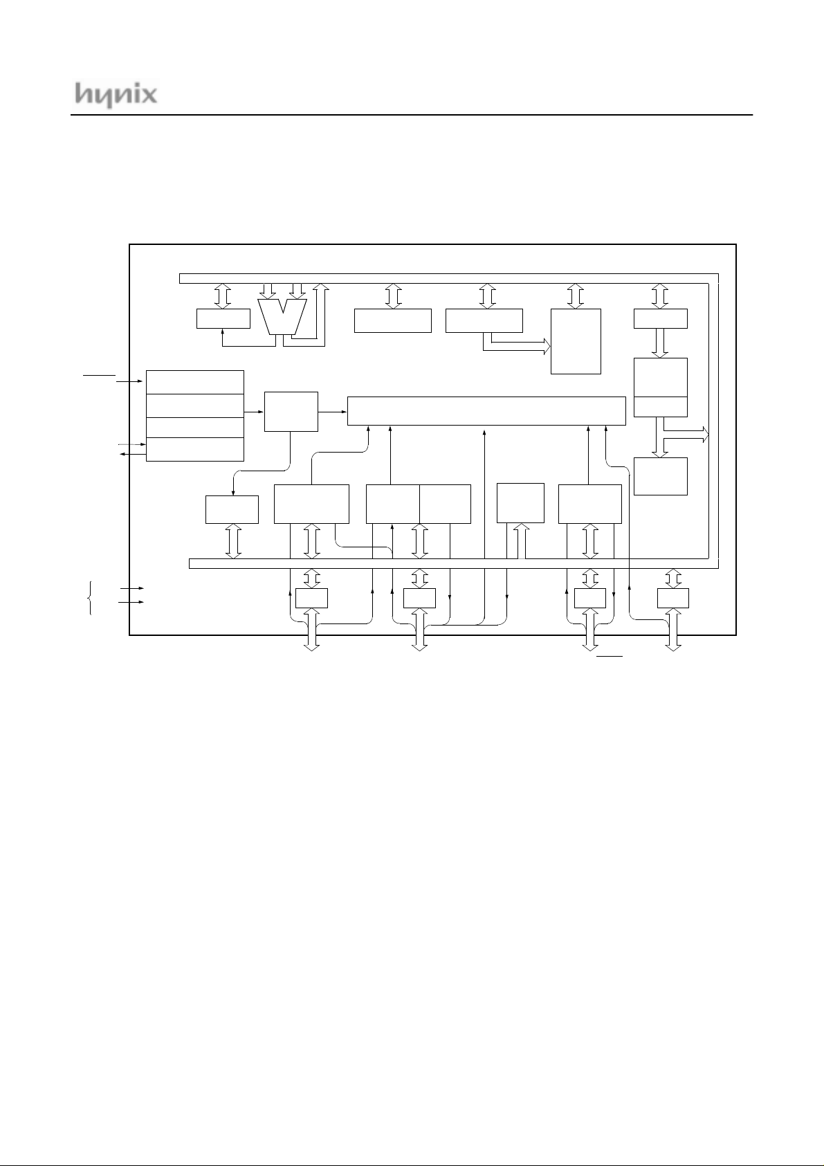
2. BLOCK DIAGRAM
GMS81C1404/GMS81C1408
RESET
Xin
Xout
V
DD
V
SS
Power
Supply
PSW
System controller
System
Clock Controller
Timing generator
Clock Generator
Watch-dog
Timer
ALU
8-bit Basic
Interval
Timer
8-bit
A/D
Converter
RA RB RC
RA0 / EC0
RA1 / AN1
RA2 / AN2
RA3 / AN3
RA4 / AN4
RA5 / AN5
RA6 / AN6
RA7 / AN7
Accumulator Stack Pointer
Interrupt Controller
8-bit
Timer/
Counter
High
Speed
PWM
RB0 / AN0 / Avref
RB1 / BUZ
RB2 / INT0
RB3 / INT1
RB4 / CMP0 / PWM0
RB5 / CMP1 / PWM1
RB6 / EC1
RB7 / TMR2OV
Buzzer
Driver
Data
Memory
SPI
RC3 / SRDY
RC4 / SCK
RC5 / SIN
RC6 / SOUT
PC
Program
Memory
Data Table
Instruction
Decoder
RD
RD0 / INT2
RD1 / INT3
RD2
June. 2001 Ver 1.2 3
Page 6
GMS81C1404/GMS81C1408
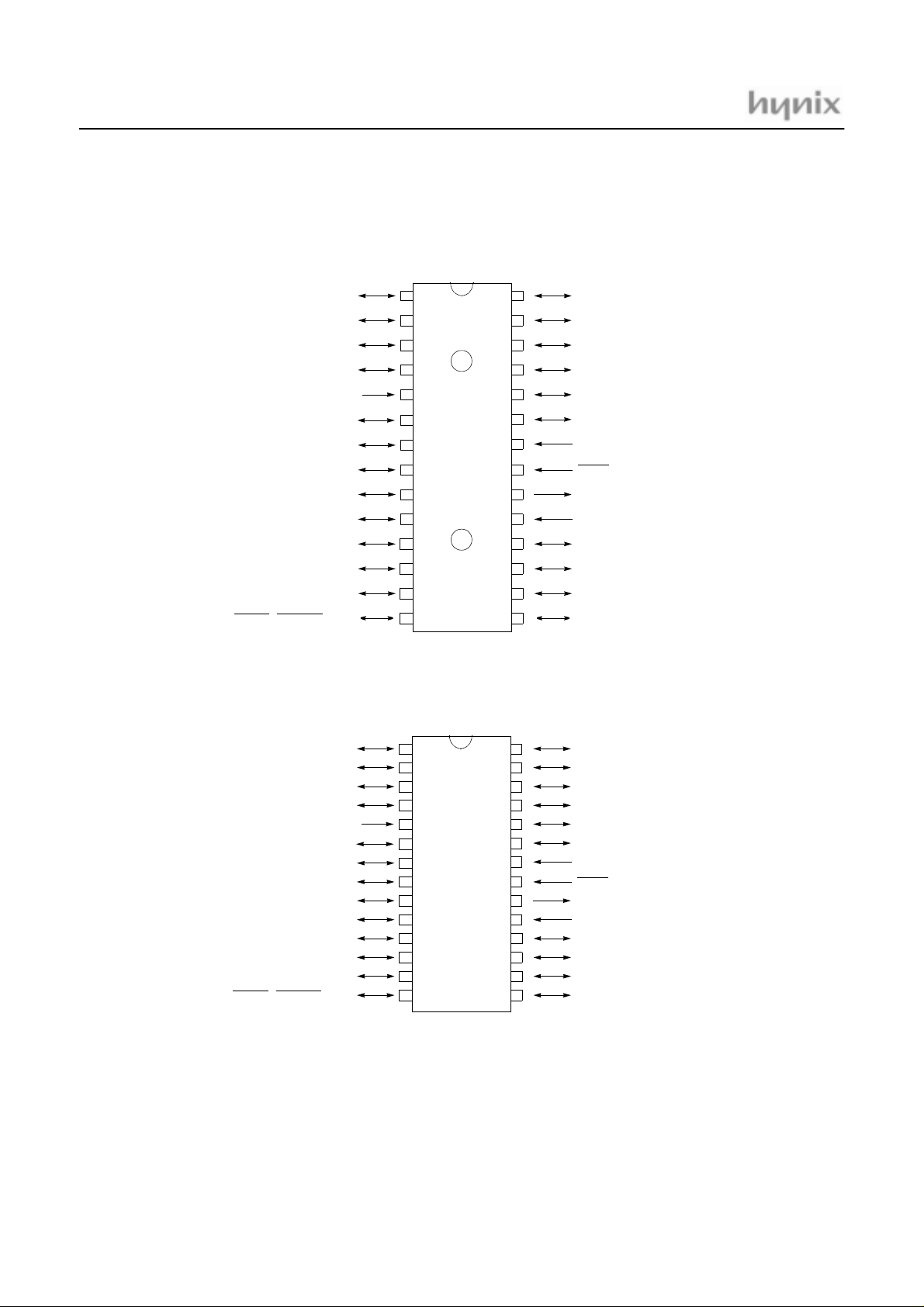
3. PIN ASSIGNMENT
28 SKINNY DIP
AN4 / RA4
AN5 / RA5
AN6 / RA6
AN7 / RA7
V
DD
AN0 / AVref / RB0
BUZ / RB1
INT0 / RB2
INT1 / RB3
PWM0 / COMP0 / RB4
PWM1 / COMP1 / RB5 RD2
EC1 / RB6
TMR2OV / RB7
SRDYIN / SRDYOUT / RC3
1
2
3
4
5
6
7
8
9
10
11
12
13
14
28
27
26
25
24
23
22
21
20
19
18
17
16
15
28 SOP
RA3 / AN3
RA2 / AN2
RA1 / AN1
RA0 / EC0
RD1 / INT3
RD0 / INT2
V
SS
RESET
Xout
Xin
RC6 / SOUT
RC5 / SIN
RC4 / SCK
AN4 / RA4
AN5 / RA5
AN6 / RA6
AN7 / RA7
V
DD
AN0 / AVref / RB0
BUZ / RB1
INT0 / RB2
INT1 / RB3
PWM0 / COMP0 / RB4
PWM1 / COMP1 / RB5 RD2
EC1 / RB6
TMR2OV / RB7
SRDYIN / SRDYOUT / RC3
1
2
3
4
5
6
7
8
9
10
11
12
13
14
28
27
26
25
24
23
22
21
20
19
18
17
16
15
RA3 / AN3
RA2 / AN2
RA1 / AN1
RA0 / EC0
RD1 / INT3
RD0 / INT2
V
SS
RESET
Xout
Xin
RC6 / SOUT
RC5 / SIN
RC4 / SCK
4
June. 2001 Ver 1.2
Page 7
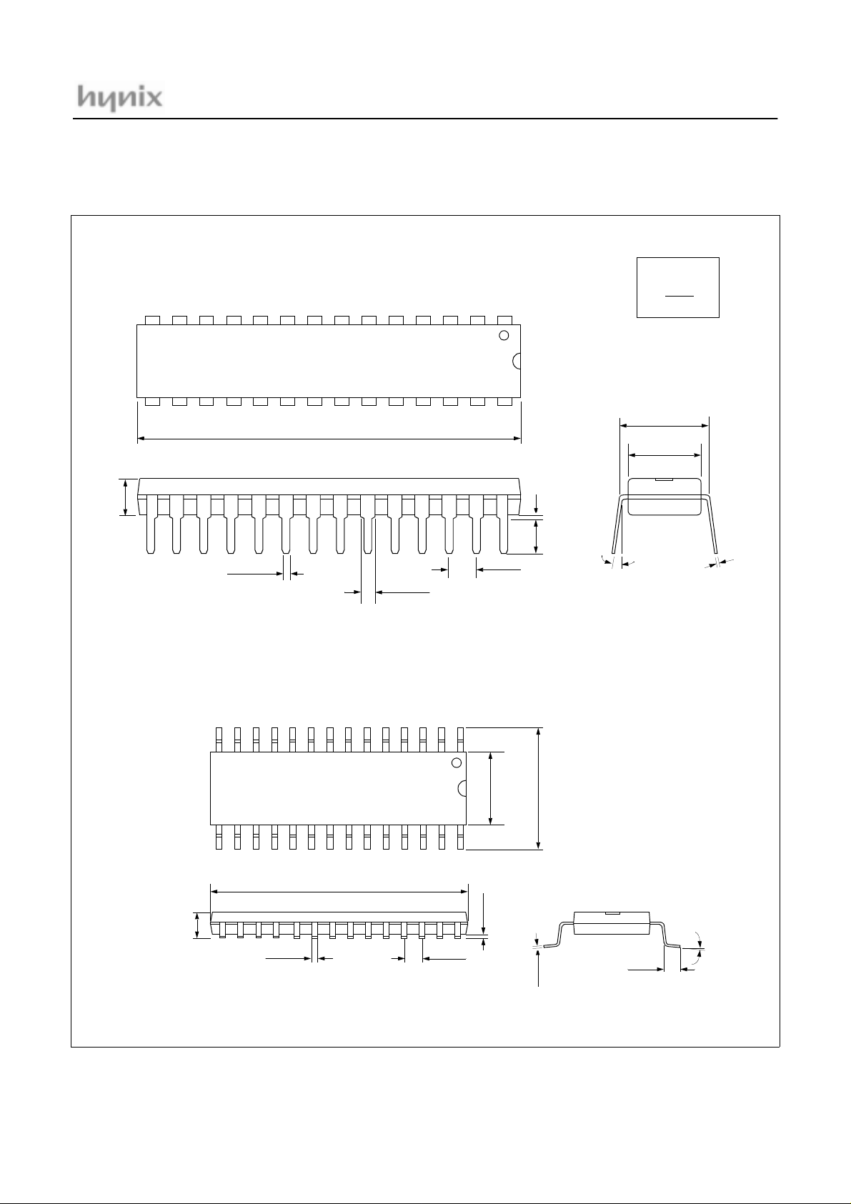
4. PACKAGE DIAGRAM
GMS81C1404/GMS81C1408
28 SKINNY DIP
MAX 0.180
0.021
0.015
1.375
1.355
0.055
0.045
TYP 0.100
0.140
MIN 0.020
0.120
0 ~ 15°
unit: inch
MAX
MIN
TYP 0.300
0.300
0.275
4
1
0
.
0
8
0
0
.
0
28 SOP
0.293
0.006
0.414
0.012
0.398
0.008
0.042
0 ~ 8°
0.022
0.299
0.708
0.608
0.012
0.106
0.096
0.019
0.013
TYP 0.050
June. 2001 Ver 1.2 5
Page 8

GMS81C1404/GMS81C1408
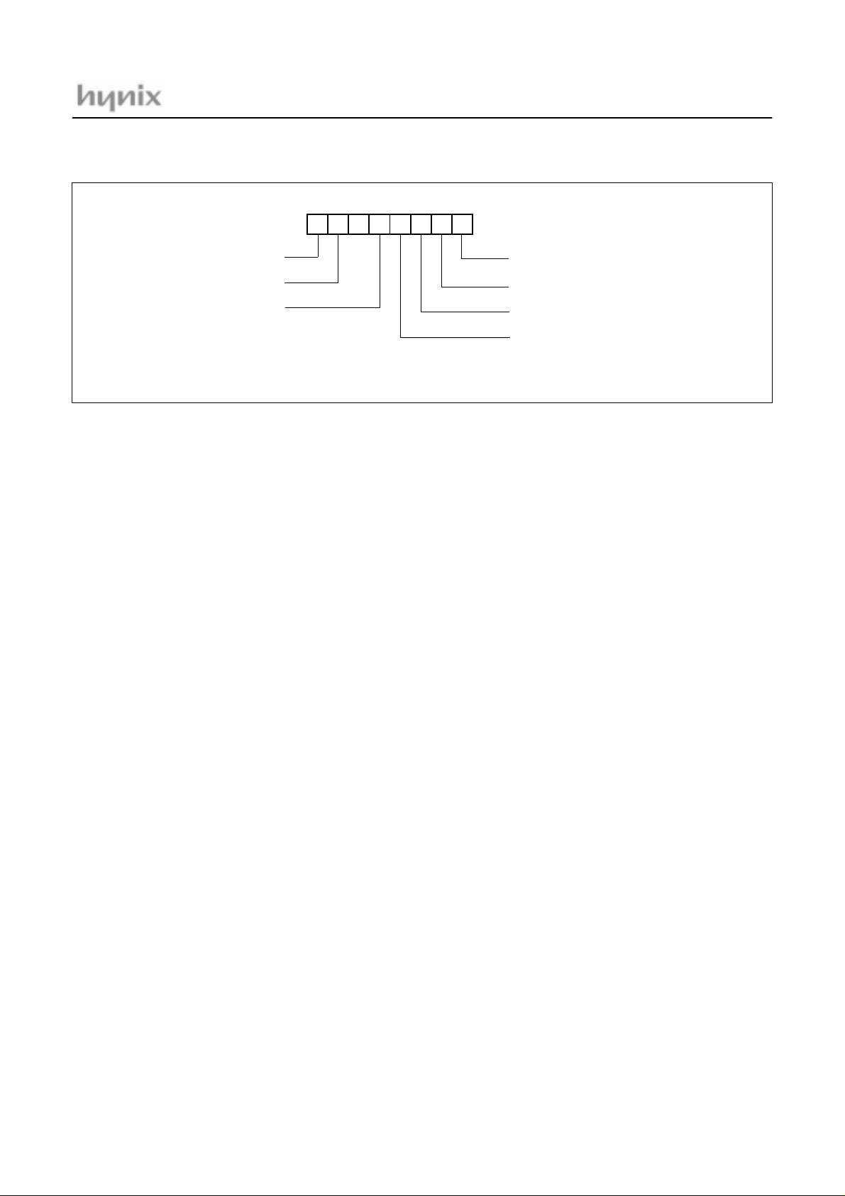
5. PIN FUNCTION
VDD: Supply voltage.
V
: Circuit ground.
SS
RESET
X
: Reset the MCU.
: Input to the inverting oscillator amplifier and input to
IN
the internal main clock operating circuit.
X
: Output from the inverting oscillator amplifier.
OUT
RA0~RA7: RA is an 8-bit, CMOS, bidirectional I/O port.
RA pins can be used as outputs or inputs according to “1”
or “0” written the their Port Direction Register(RAIO).
Port pin Alternate function
RA0
RA1
RA2
RA3
RA4
RA5
RA6
RA7
EC0 ( Event Counter Input Source )
AN1 ( Analog Input Port 1 )
AN2 ( Analog Input Port 2 )
AN3 ( Analog Input Port 3 )
AN4 ( Analog Input Port 4 )
AN5 ( Analog Input Port 5 )
AN6 ( Analog Input Port 6 )
AN7 ( Analog Input Port 7 )
Table 5-1 RA Port
In addition, RA serves the functions of the various special
features in Table 5-1 .
RB0~RB7: RB is a 8-bit, CMOS, bidirectional I/O port.
RB pins can be used as outputs or inputs according to “1”
or “0” written the their Port Direction Register(RBIO).
RC3~RC6: RC is a 4-bit, CMOS, bidirectional I/O port.
RC pins can be used as outputs or inputs according to “1”
or “0” written the their Port Direction Register(RCIO).
RC serves the functions of the serial interface following
special features in Table 5-3 .
Port pin Alternate function
RC3
RC4
RC5
RC6
SRDYIN
SRDYOUT
SCKI (SPI CLK Input)
SCKO (SPI CLK Output)
SIN (SPI Serial Data Input)
SOUT (SPI Serial Data Output)
(SPI Ready Input)
(SPI Ready Output)
Table 5-3 RC Port
RD0~RD2: RD is a 3-bit, CMOS, bidirectional I/O port.
RC pins can be used as outputs or inputs according to “1”
or “0” written the their Port Direction Register(RDIO).
RD serves the functions of the external interrupt following
special features in Table 5-4
Port pin Alternate function
RD0
RD1
RD2
INT2 (External Interrupt Input Port 2)
INT3 (External Interrupt Input Port 3)
Table 5-4 RD Port
RB serves the functions of the va rious following special
features
in
Table 5-2
Port pin Alternate function
RB0
RB1
RB2
RB3
RB4
RB5
RB6
RB7
AN0 ( Analog Input Port 0 )
AVref ( External Analog Reference Pin )
BUZ ( Buzzer Driving Output Port )
INT0 ( External Interrupt Input Port 0 )
INT1 ( External Interrupt Input Port 1 )
PWM0 (PWM0 Output)
COMP0 (Timer1 Compare Output)
PWM1 (PWM1 Output)
COMP1 (Timer3 Compare Output)
EC1 (Event Counter Input Source)
TMR2OV (Timer2 Overflow Output)
Table 5-2 RB Port
6
June. 2001 Ver 1.2
Page 9
PIN NAME Pin No. In/Out Function
V
DD
V
SS
RESET
X
IN
X
OUT
22
21
19
20
RA0 (EC0) 25
RA1 (AN1) 26
RA2 (AN2) 27
RA3 (AN3) 28
RA4 (AN4) 1
RA5 (AN5) 2
RA6 (AN6) 3
RA7 (AN7) 4
RB0 (AVref/AN0) 6
RB1 (BUZ) 7
RB2 (INT0) 8
RB3 (INT1) 9
RB4 (PWM0/COMP0) 10
RB5 (PWM1/COMP1) 11
RB6 (EC1) 12
RB7 (TMR2OV) 13
RC3 (SRDYIN
/SRDYOUT)14
RC4 (SCK) 15
RC5 (SIN) 16
RC6 (SOUT) 17
RD0 (INT2) 23
RD1 (INT3) 24
RD2 18
5
-
I
I
O
I/O (Input)
I/O (Input)
I/O (Input)
I/O (Input)
I/O (Input)
I/O (Input)
I/O (Input)
I/O (Input)
I/O (Input)
I/O (Input)
I/O (Input)
I/O (Output)
I/O (Output/Output)
I/O (Output/Output)
I/O (Output/Output)
I/O (Output/Output)
I/O (Input/Output)
I/O (Input/Output)
I/O (Input)
I/O (Output)
I/O (Input)
I/O (Input)
I/O
Supply voltage
Circuit ground
Reset signal input
8-bit general I/O ports
8-bit general I/O ports
4-bit general I/O ports
3-bit general I/O ports
GMS81C1404/GMS81C1408
External Event Counter input 0
Analog Input Port 1
Analog Input Port 2
Analog Input Port 3
Analog Input Port 4
Analog Input Port 5
Analog Input Port 6
Analog Input Port 7
Analog Input Port 0 / Analog Reference
Buzzer Driving Output
External Interrupt Input 0
External Interrupt Input 1
PWM0 Output or Timer1 Compare Output
PWM1 Output or Timer3 Compare Output
External Event Counter input 1
Timer2 Overflow Output
SPI READY Input/Output
SPI CLK Input/Output
SPI DATA Input
SPI DATA Output
External Interrupt Input 2
External Interrupt Input 3
Table 5-5 Pin Description
June. 2001 Ver 1.2 7
Page 10
GMS81C1404/GMS81C1408
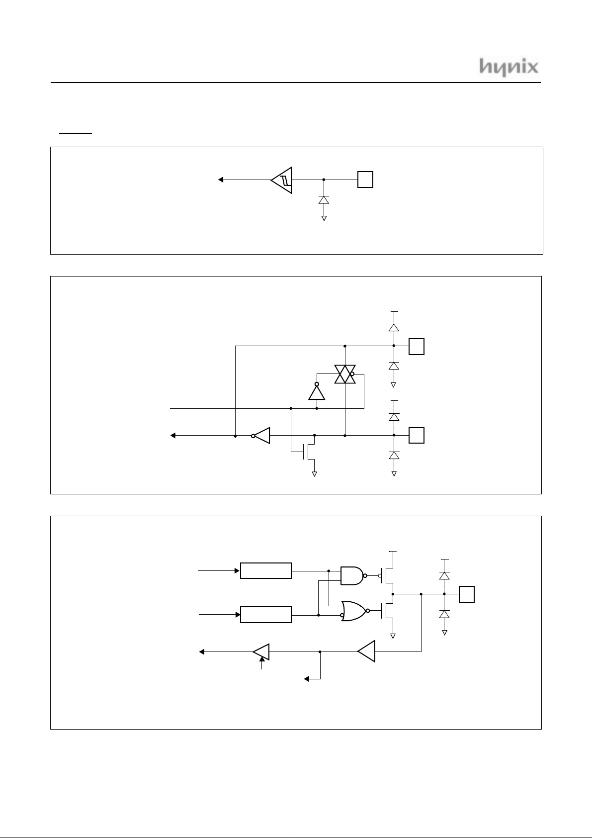
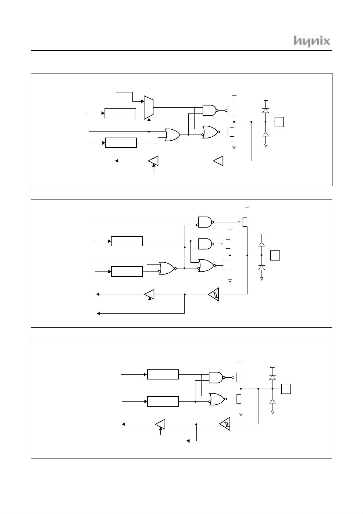
6. PORT STRUCTURES
• RESET
Internal RESET
• Xin, Xout
V
SS
V
DD
Xout
• RA0/EC0
STOP
To System CLK
Data Bus
Data Bus
Data Bus
Data Reg.
Direction Reg.
Read
EC0
V
SS
Xin
8
June. 2001 Ver 1.2
Page 11
• RA1/AN1 ~ RA7/AN7
Data Bus
Data Bus
Data Bus
To A/D Converter
Analog Input Mode
(ANSEL7 ~ 1)
Analog CH. Selection
(ADCM.4 ~ 2)
Data Reg.
Direction Reg.
Read
GMS81C1404/GMS81C1408
V
DD
V
SS
• RB0 / AN0 / AVref
Data Bus
AVREFS
Data Bus
Data Bus
To A/D Converter
Analog Input Mode
(ANSEL0)
Analog CH0 Selection
(ADCM.4 ~ 2)
Read
Data Reg.
Direction Reg.
To Vref of A/D
1
0
AVREFS
V
DD
V
SS
Internal V
DD
June. 2001 Ver 1.2 9
Page 12
GMS81C1404/GMS81C1408
• RB1/BUZ, RB4/PWM0/COMP0, RB5/PWM1/COMP1, RB7/TMR2OV, RC6/SOUT
PWM/COMP
BUZ,TMR2OV,SOUT
1
0
Read
Data Bus
Function
Select
Data Bus
Data Reg.
Direction Reg.
Data Bus
• RB2/INT0, RB3/INT1, RD0/INT2, RD1/INT3
Pull-up
Select
V
V
SS
DD
Weak Pull-up
• RB6/EC1
Data Bus
Function
Select
Data Bus
Data Bus
INT0, INT1
INT2, INT3
Data Bus
Data Bus
Data Reg.
Direction Reg.
Read
Data Reg.
Direction Reg.
Schmitt Trigger
V
DD
V
SS
10
Data Bus
Read
EC1
June. 2001 Ver 1.2
Page 13
• RD2
• RC5/SIN
Data Bus
Data Bus
Data Bus
Data Reg.
Direction Reg.
Read
GMS81C1404/GMS81C1408
V
DD
V
SS
Data Bus
Function
Select
Data Bus
Data Bus
• RC3 / SRDYIN
Data Bus
Function
Select
Data Bus
Data Bus
Data Reg.
Direction Reg.
Read
SIN
/ SRDYOUT, RC4 / SCKIN / SCKOUT
SRDYOUT
SCKOUT
Data Reg.
Direction Reg.
1
0
Schmitt Trigger
V
DD
V
SS
V
DD
V
SS
Read
SCKIN
SRDYIN
Schmitt Trigger
June. 2001 Ver 1.2 11
Page 14
GMS81C1404/GMS81C1408
7. ELECTRICAL CHARACTERISTICS (GMS81C1404/GMS81C1408)
7.1 Absolute Maximum Ratings
Supply voltage...........................................-0.3 to +6.0 V
Storage Temperature ................................-40 to +125 °C
Voltage on any pin with respect to Ground (V
SS
)
................................ ............................... -0.3 to VDD+0.3
Maximum current out of V
Maximum current into V
Maximum current sunk by (I
Maximum output current sourced by (I
pin........................200 mA
SS
pin ..........................150 mA
DD
per I/O Pin) ........25 mA
OL
per I/O Pin)
OH
...............................................................................15 mA
Maximum current (ΣI
) ....................................150 mA
OL
7.2 Recommended Operating Conditions
Maximum current (ΣI
Stresses above those listed under “Absolute Maxi-
Note:
mum Ratings” may cause perma nent damage to the
device. This is a stress rat ing only and functional op eration of the device at any other conditions above
those indicated in the operational sections of this
specification is not implied. Exposure to absolute
maximum rating cond itions for extended pe riods
may affect device reliability.
)....................................100 mA
OH
Parameter Symbol Condition
Supply Voltage
Operating Frequency
Operating Temperature
V
T
f
XIN
OPR
DD
7.3 A/D Converter Characteristics
(TA=25°C, VSS=0V, VDD=5.12V @
Parameter Symbol Condition
Analog Input Voltage Range
Analog Power Supply Input Voltage Range
Overall Accuracy
Non-Linearity Error
Differential Non-Linearity Error
Zero Offset Error
Full Scale Error
Gain Error
Conversion Time
AV
Input Current I
REF
f
=8MHz, VDD=3.072V @
XIN
f
=8MHz
XIN
=4.2MHz
f
XIN
VDD=4.5~5.5V
V
=2.2~5.5V
DD
V
AIN
V
REF
N
ACC
N
NLE
N
DNLE
N
ZOE
N
FSE
N
NLE
T
CONV
REF
Specifications
Unit
Min. Max.
4.5 5.5 V
2.2 5.5 V
18MHz
14.2MHz
-20 (-40 for GMS81C140XE) 85
f
=4MHz)
XIN
C
°
Specifications
Unit
Min. Typ. Max.
AVREFS=0
AVREFS=1
VDD=5V
V
=3V
DD
f
=8MHz
XIN
f
=4MHz
XIN
V
SS
V
SS
-
-
3-
2.4 -
-
-
-
-
-
-
±
±
±
±
±
±
1.0
1.0
1.0
0.5
0.25
1.0
--10
--20
V
DD
V
REF
V
DD
V
DD
1.5 LSB
±
1.5 LSB
±
1.5 LSB
±
1.5 LSB
±
0.5 LSB
±
1.5 LSB
±
V
V
V
µ
AVREFS=1 - 0.5 1.0 mA
S
12
June. 2001 Ver 1.2
Page 15
7.4 DC Electrical Characteri stics
GMS81C1404/GMS81C1408
(TA=-20~85°C for GMS81C1404/1408 or TA=-40~85°C for GMS81C1404E/1408E, VDD=2.2~5.5V, VSS=0V)
Parameter Symbol Pin Condition
XIN, RESET 0.8 V
IH1
Hysteresis Input
IH2
Normal Input
IH3
XIN, RESET
IL1
Hysteresis Input
IL2
Normal Input 0 -
IL3
All Output Port
OH
All Output Port
OL
I
RB2, RB3, RD0, RD1
P
All Pins (except XIN)VDD=5V
IH1
X
IH2
IL1
IL2
T
IN
All Pins (except XIN)VDD=5V
X
IN
|
Hysteresis Input
1
1
VDD=5V, IOH=-5mA VDD -1
VDD=5V, IOL=10mA
VDD=5V
VDD=5V
VDD=5V
1
VDD=5V
PFD Level = 0 2.5 3.0 3.5
PFD Level = 1 2.0 2.5 3.0
VDD=5V
V
DD
Input High Voltage
Input Low Voltage
Output High Voltage
Output Low Voltage
Input Pull-up Current
Input High
Leakage Current
Input Low
Leakage Current
Hysteresis
PFD Voltage
Internal RC WDT
Period
V
V
V
V
V
V
V
V
I
I
I
I
| V
V
PFD1VDD
V
PFD2VDD
T
RCWDT
VDD=5.5V, f
Operating Current
Wake-up Timer
Mode Current
RCWDT Mode
Current at STOP
Mode
I
I
WKUPVDD
I
RCWDTVDD
DD
V
DD
V
DD
VDD=5.5V, f
V
DD
VDD=5.5V
V
DD
VDD=5.5V, f
Stop Mode Current
1. Hysteresis Input: RB2, RB3, RB6, RC3, RC4, RC5, RD0, RD1
I
STOP
V
DD
V
DD
=3V
=3.0V, f
=3.0V, f
=3.0V
=3.0V, f
XIN
XIN
XIN
XIN
XIN
XIN
=8MHz
=4MHz
=8MHz
=4MHz
=8MHz
=4MHz
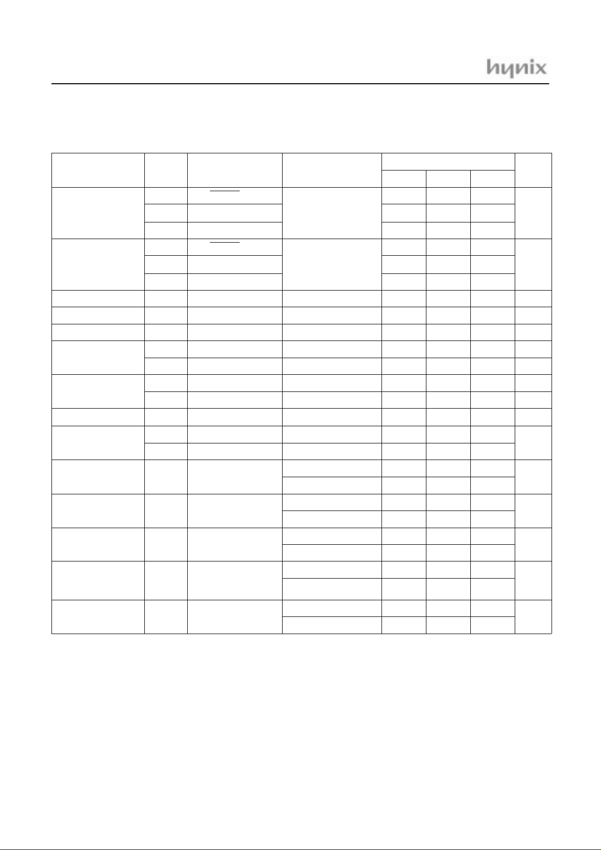
Specifications
Min. Typ. Max.
-
-
-
0.8 V
0.7 V
DD
DD
DD
00-
V
V
V
0.2 V
0.2 V
DD
DD
DD
0.3 V
--V
-
-1V
-550 -320 -200
--5µA
--15µA
-5 - -
-15 - -
0.5 - - V
30 120
60 280
-56
-23
-12
-0.51
--200
--100
-0.53
-0.21
DD
DD
DD
,
Unit
V
V
A
µ
A
µ
A
µ
V
S
µ
mA
mA
A
µ
A
µ
June. 2001 Ver 1.2 13
Page 16
GMS81C1404/GMS81C1408
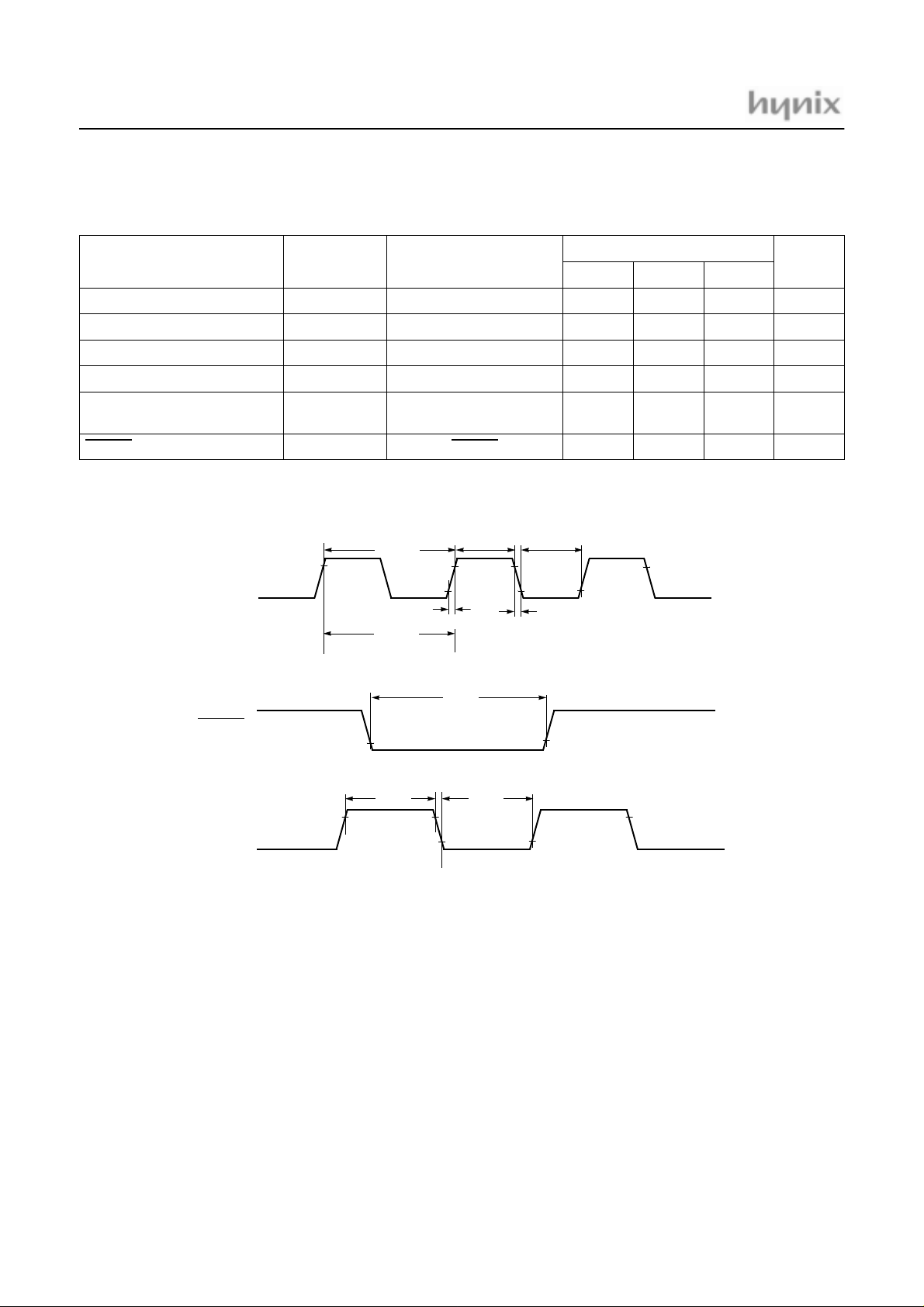
7.5 AC Characteristics
(TA=-20~85°C for GMS81C1404/1408 or TA=-40~85°C for GMS81C1404E/1408E, VDD=5V±10%, VSS=0V)
Parameter Symbol Pins
Operating Frequency
External Clock Pulse Width
External Clock Transition Time
Oscillation Stabilizing Time
External Input Pulse Width
RESET Input Width
X
IN
f
CP
t
CPW
t
RCP,tFCP
t
ST
t
EPW
t
RST
X
IN
X
IN
X
IN
XIN, X
OUT
INT0, INT1, INT2, INT3
EC0, EC1
RESET 8--
t
t
1/f
SYS
CP
t
RCP
t
CPW
RST
t
FCP
t
CPW
Specifications
Unit
Min. Typ. Max.
1-8MHz
80 - - nS
- - 20 nS
--20mS
2--
-0.5V
V
DD
0.5V
t
t
SYS
SYS
RESET
INT0, INT1
INT3
INT2,
EC0,
EC1
t
EPW
t
EPW
Figure 7-1 Timing Chart
0.2V
0.2V
DD
DD
0.8V
DD
14
June. 2001 Ver 1.2
Page 17
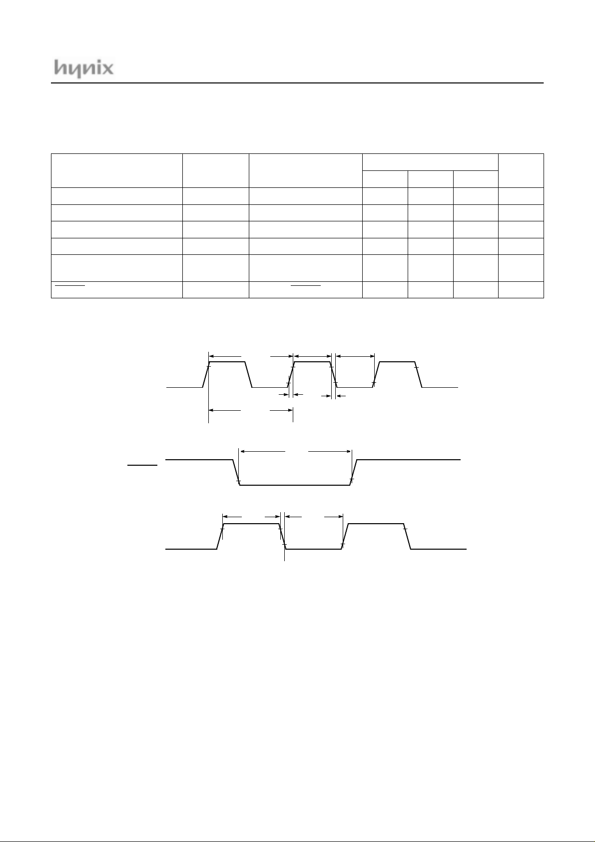
7.6 Typical Characteristics
GMS81C1404/GMS81C1408
This graphs and tables provided in this section are for design guidance only and are not tested or guaranteed.
In some graphs or tables the data presented are outside specified operating range (e.g. outside specified
VDD range). This is for information only and devices
are guaranteed to operate properly only within the
specified range.
Operating Area
f
XIN
(MHz)
Ta= 25°C
10
8
6
4
2
0
23
45
V
DD
(V)
6
STOP Mode
I
DD
(µA)
I
0.8
0.6
0.4
STOP
f
= 8MHz
XIN
V
−
DD
-40°C
25°C
85°C
The data presented in this s ection is a statistical s ummary
of data collected on units from different lots over a period
of time. “Typical” represents the mean of the distribution
while “max” or “min” represents (mean + 3σ) and (mean −
3σ) respectively where σ is standard deviation
Normal Operation
I
V
−
DD
Ta=25°C
23
DD
f
XIN
= 8MHz
4MHz
45
V
DD
(V)
6
I
DD
(mA)
8
6
4
2
0
Wake-up Timer Mode
I
DD
(mA)
2.0
1.5
1.0
I
WKUP
Ta=25°C
−
f
XIN
V
DD
= 8MHz
0.2
0
23
45
V
DD
(V)
6
0.5
0
23
4MHz
45
V
DD
(V)
6
RC-WDT in Stop Mode
I
DD
(µA)
20
15
10
5
0
I
RCWDT
Ta=25°C
23
V
−
T
RCWDT
DD
= 80uS
45
V
DD
(V)
6
June. 2001 Ver 1.2 15
Page 18
GMS81C1404/GMS81C1408
I
OL
I
OL
(mA)
40
30
20
10
0
V
V
−
DD
IH1
V
IH1
f
=4MHz
XIN
(V)
Ta=25°C
4
3
2
, VDD=5V
V
−
OL
12345
XIN, RESET
I
OH
I
OH
-40°C
25°C
85°C
V
OL
(V)
V
V
−
DD
IH2
V
IH2
f
=4kHz
XIN
(V)
Ta=25°C
4
3
2
(mA)
-20
-15
-10
-5
0
Hysteresis input
, VDD=5V
V
−
OH
V
23456
V
V
−
DD
IH3
V
IH3
f
=4kHz
XIN
(V)
Ta=25°C
4
3
2
-40°C
OH
(V)
Normal input
25°C
85°C
V
(V)
IL2
1
0
V
4
3
2
1
0
23
V
−
DD
f
=4kHz
XIN
Ta=25°C
23
45
IL2
Hysteresis input
45
V
DD
(V)
6
V
DD
(V)
6
1
0
1
23
V
V
−
DD
V
IL1
f
=4MHz
XIN
(V)
Ta=25°C
4
3
2
1
0
1
23
45
IL1
XIN, RESET
45
V
DD
(V)
6
V
DD
(V)
6
V
(V)
IL3
1
0
V
4
3
2
1
0
23
V
−
DD
f
=4kHz
XIN
Ta=25°C
23
IL3
Normal input
45
45
V
DD
(V)
6
V
DD
(V)
6
16
June. 2001 Ver 1.2
Page 19
GMS81C1404/GMS81C1408
8. ELECTRICAL CHARACTERISTICS (GMS87C1404/GMS87C1408)
8.1 Absolute Maximum Ratings
Supply voltage...........................................-0.3 to +6.0 V
Storage Temperature ................................-40 to +125 °C
Voltage on any pin with respect to Ground (V
SS
)
................................ ............................... -0.3 to VDD+0.3
Maximum current out of V
Maximum current into V
Maximum current sunk by (I
Maximum output current sourced by (I
pin........................200 mA
SS
pin ..........................150 mA
DD
per I/O Pin) ........25 mA
OL
per I/O Pin)
OH
...............................................................................15 mA
Maximum current (ΣI
) ....................................150 mA
OL
8.2 Recommended Operating Conditions
Maximum current (ΣI
Note: Stresses above those listed under “Absolute Maxi-
mum Ratings” may cause perma nent damage to the
device. This is a stress rat ing only and functional op eration of the device at any other conditions above
those indicated in the operational sections of this
specification is not implied. Exposure to absolute
maximum rating cond itions for extended pe riods
may affect device reliability.
)....................................100 mA
OH
Parameter Symbol Condition
T
V
f
XIN
OPR
DD
Supply Voltage
Operating Frequency
Operating Temperature
8.3 A/D Converter Characteristics
(TA=25°C, VSS=0V, VDD=5.12V @
Parameter Symbol Condition
Analog Input Voltage Range
Analog Power Supply Input Voltage Range
Overall Accuracy
Non-Linearity Error
Differential Non-Linearity Error
Zero Offset Error
Full Scale Error
Gain Error
Conversion Time
AV
Input Current I
REF
f
=8MHz, VDD=3.072V @
XIN
f
=8MHz
XIN
=4.2MHz
f
XIN
VDD=4.5~5.5V
V
=2.5~5.5V
DD
V
AIN
V
REF
N
ACC
N
NLE
N
DNLE
N
ZOE
N
FSE
N
NLE
T
CONV
REF
Specifications
Unit
Min. Max.
4.5 5.5 V
2.5 5.5 V
18MHz
14.2MHz
f
XIN
-20 85
=4MHz)
C
°
Specifications
Unit
Min. Typ. Max.
AVREFS=0
AVREFS=1
VDD=5V
V
=3V
DD
f
=8MHz
XIN
f
=4MHz
XIN
V
SS
V
SS
-
-
3-
2.4 -
-
-
-
-
-
-
±
±
±
±
±
±
1.0
1.0
1.0
0.5
0.25
1.0
--10
--20
V
DD
V
REF
V
DD
V
DD
1.5 LSB
±
1.5 LSB
±
1.5 LSB
±
1.5 LSB
±
0.5 LSB
±
1.5 LSB
±
V
V
V
µ
AVREFS=1 - 0.5 1.0 mA
S
June. 2001 Ver 1.2 17
Page 20
GMS81C1404/GMS81C1408
8.4 DC Electrical Characteri stics
(TA=-20~85°C, VDD=2.5~5.5V, VSS=0V)
,
Parameter Symbol Pin Condition
XIN, RESET 0.8 V
IH1
Hysteresis Input
IH2
Normal Input
IH3
XIN, RESET
IL1
Hysteresis Input
IL2
Normal Input 0 -
IL3
All Output Port
OH
All Output Port
OL
I
RB2, RB3, RD0, RD1
P
All Pins (except XIN)VDD=5V
IH1
X
IH2
IL1
IL2
T
IN
All Pins (except XIN)VDD=5V
X
IN
|
Hysteresis Input
1
1
VDD=5V, IOH=-5mA VDD -1
VDD=5V, IOL=10mA
VDD=5V
VDD=5V
VDD=5V
1
VDD=5V
PFD Level = 0 2.5 3.0 3.5
PFD Level = 1 2.0 2.5 3.0
VDD=5V
V
DD
Input High Voltage
Input Low Voltage
Output High Voltage
Output Low Voltage
Input Pull-up Current
Input High
Leakage Current
Input Low
Leakage Current
Hysteresis
PFD Voltage
Internal RC WDT
Period
V
V
V
V
V
V
V
V
I
I
I
I
| V
V
PFD1VDD
V
PFD2VDD
T
RCWDT
VDD=5.5V, f
Operating Current
Wake-up Timer
Mode Current
RCWDT Mode
Current at STOP
Mode
I
I
WKUPVDD
I
RCWDTVDD
DD
V
DD
V
DD
VDD=5.5V, f
V
DD
VDD=5.5V
V
DD
VDD=5.5V, f
Stop Mode Current
1. Hysteresis Input: RB2, RB3, RB6, RC3, RC4, RC5, RD0, RD1
I
STOP
V
DD
V
DD
=3V
=3.0V, f
=3.0V, f
=3.0V
=3.0V, f
XIN
XIN
XIN
XIN
XIN
XIN
=8MHz
=4MHz
=8MHz
=4MHz
=8MHz
=4MHz
Specifications
Min. Typ. Max.
-
-
-
0.8 V
0.7 V
DD
DD
DD
00-
V
V
V
0.2 V
0.2 V
0.3 V
DD
DD
DD
DD
DD
DD
--V
-
-1V
-550 -420 -200
--5µA
--15µA
-5 - -
-15 - -
0.5 - - V
40 120
95 280
-56
-23
-12
-0.51
--200
--100
-0.53
-0.21
Unit
V
V
A
µ
A
µ
A
µ
V
S
µ
mA
mA
A
µ
A
µ
18
June. 2001 Ver 1.2
Page 21
8.5 AC Characteristics
(TA=-20~+85°C, VDD=5V±10%, VSS=0V)
GMS81C1404/GMS81C1408
Parameter Symbol Pins
Operating Frequency
External Clock Pulse Width
External Clock Transition Time
Oscillation Stabilizing Time
External Input Pulse Width
RESET Input Width
X
IN
f
CP
t
CPW
t
RCP,tFCP
t
ST
t
EPW
t
RST
X
IN
X
IN
X
IN
XIN, X
OUT
INT0, INT1, INT2, INT3
EC0, EC1
RESET 8--
t
t
1/f
SYS
CP
t
RCP
t
CPW
RST
t
FCP
t
CPW
Specifications
Unit
Min. Typ. Max.
1-8MHz
80 - - nS
- - 20 nS
--20mS
2--
-0.5V
V
DD
0.5V
t
t
SYS
SYS
RESET
INT0, INT1
INT3
INT2,
EC0,
EC1
t
EPW
t
EPW
Figure 8-1 Timing Chart
0.2V
0.2V
DD
DD
0.8V
DD
June. 2001 Ver 1.2 19
Page 22

GMS81C1404/GMS81C1408
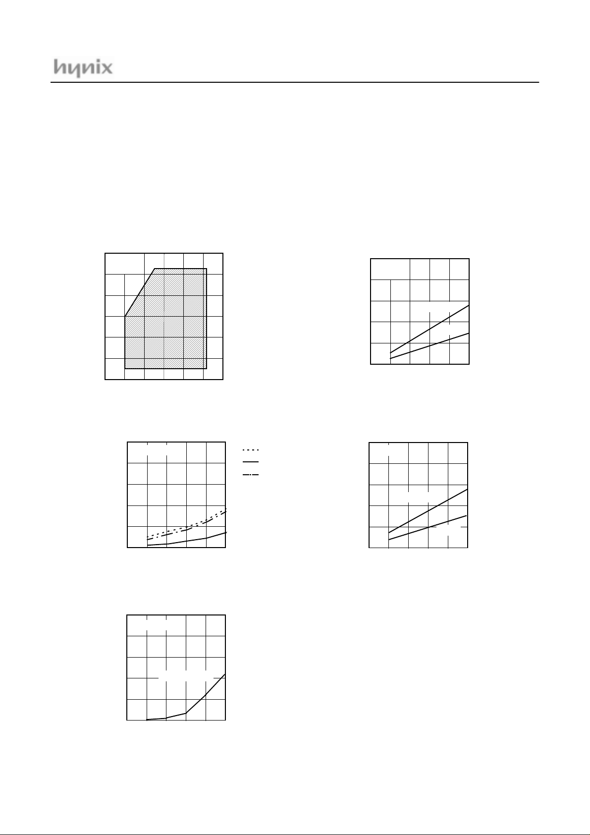
8.6 Typical Characteristics
This graphs and tables provided in this section are for design guidance only and are not tested or guaranteed.
In some graphs or tables the data presented are outside specified operating range (e.g. outside specified
VDD range). This is for information only and devices
are guaranteed to operate properly only within the
specified range.
Operating Area
f
XIN
(MHz)
Ta= 25°C
10
8
6
4
2
0
23
45
V
DD
(V)
6
STOP Mode
I
DD
(µA)
I
0.8
0.6
0.4
STOP
f
= 8MHz
XIN
V
−
DD
-25°C
25°C
85°C
The data presented in this s ection is a statistical s ummary
of data collected on units from different lots over a period
of time. “Typical” represents the mean of the distribution
while “max” or “min” represents (mean + 3σ) and (mean −
3σ) respectively where σ is standard deviation
Normal Operation
I
V
−
DD
Ta=25°C
23
DD
f
XIN
= 8MHz
4MHz
45
V
DD
(V)
6
I
DD
(mA)
8
6
4
2
0
Wake-up Timer Mode
I
DD
(mA)
2.0
1.5
1.0
I
WKUP
Ta=25°C
V
−
DD
f
= 8MHz
XIN
20
0.2
0
23
RC-WDT in Stop Mode
I
DD
(µA)
20
15
10
5
0
I
RCWDT
Ta=25°C
23
V
−
T
RCWDT
DD
45
= 80uS
45
0.5
V
DD
(V)
6
V
DD
(V)
6
0
23
4MHz
V
DD
(V)
45
6
June. 2001 Ver 1.2
Page 23
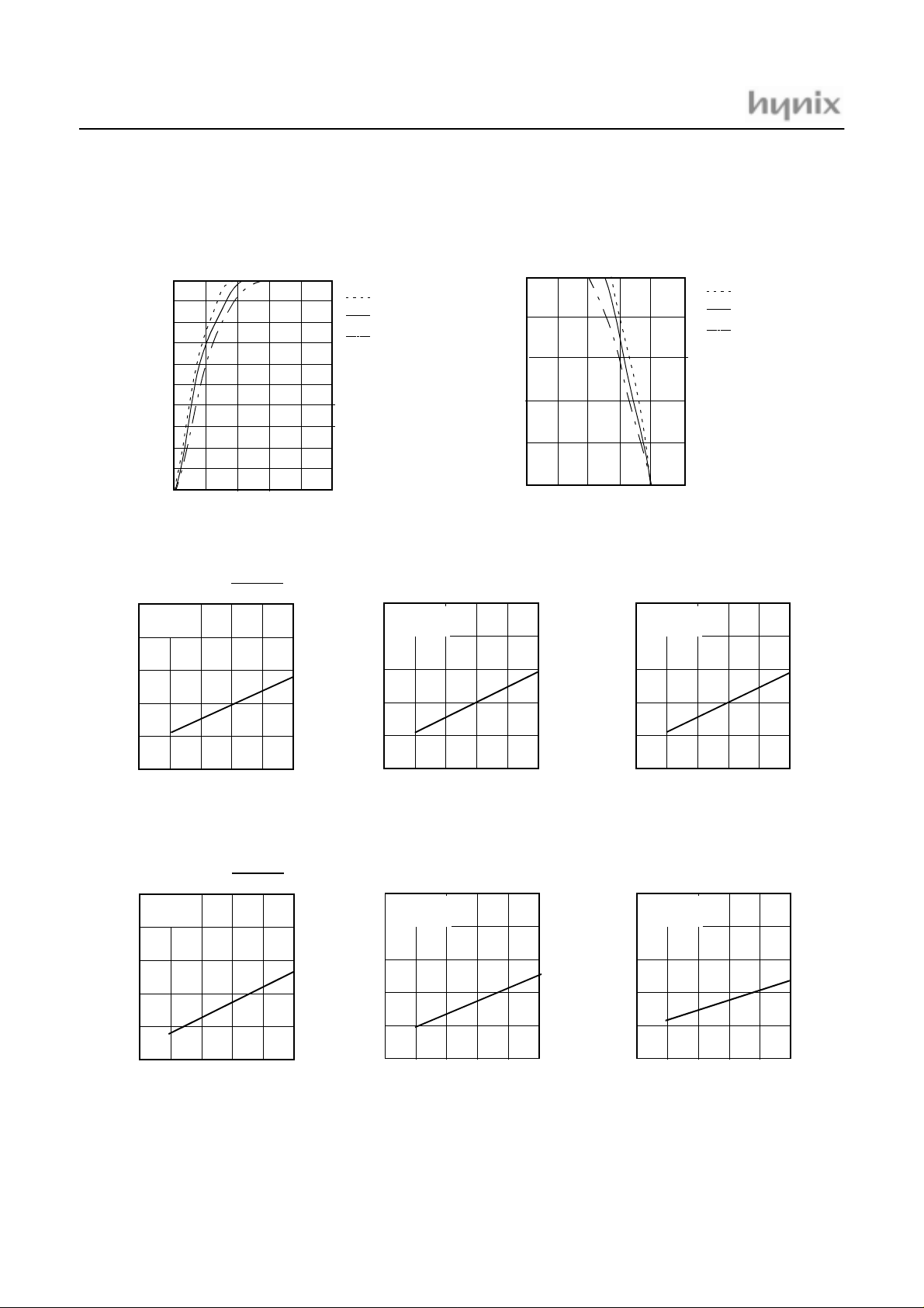
GMS81C1404/GMS81C1408
I
OL
I
OL
(mA)
40
30
20
10
0
V
V
−
DD
IH1
V
IH1
f
=4MHz
XIN
(V)
Ta=25°C
4
3
2
, VDD=5V
V
−
OL
12345
XIN, RESET
I
OH
I
OH
-25°C
25°C
85°C
V
OL
(V)
V
V
−
DD
IH2
V
IH2
f
=4kHz
XIN
(V)
Ta=25°C
4
3
2
(mA)
-20
-15
-10
-5
0
Hysteresis input
, VDD=5V
V
−
OH
V
23456
V
V
−
DD
IH3
V
IH3
f
=4kHz
XIN
(V)
Ta=25°C
4
3
2
-25°C
OH
(V)
Normal input
25°C
85°C
V
(V)
IL2
1
0
V
4
3
2
1
0
23
V
−
DD
f
=4kHz
XIN
Ta=25°C
23
45
IL2
Hysteresis input
45
V
DD
(V)
6
V
DD
(V)
6
1
0
1
23
V
V
−
DD
V
IL1
f
=4MHz
XIN
(V)
Ta=25°C
4
3
2
1
0
1
23
45
IL1
XIN, RESET
45
V
DD
(V)
6
V
DD
(V)
6
V
(V)
IL3
1
0
V
4
3
2
1
0
23
V
−
DD
f
=4kHz
XIN
Ta=25°C
23
IL3
Normal input
45
45
V
DD
(V)
6
V
DD
(V)
6
June. 2001 Ver 1.2 21
Page 24
GMS81C1404/GMS81C1408
9. MEMORY ORGANIZATION
The GMS81C1404 and GMS81C1408 have separate address spaces for Program memory and Data Memory. Pro gram memory can only be read, not written to. It can be up
9.1 Registers
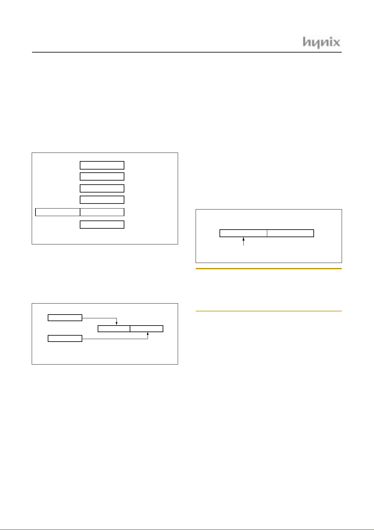
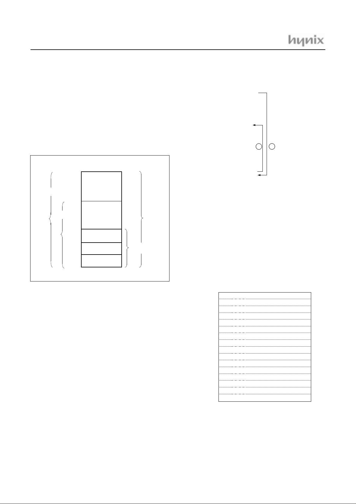
This device has six registers that are the Program Counter
(PC), a Accumulator (A), two index registers (X, Y), the
Stack Pointer (SP), and the Program Status Word (PSW).
The Program Counter consists of 16-bit register.
A
X
Y
SP
PCLPCH
PSW
Figure 9-1 Configuration of Registers
Accumulator: The Accumulato r is the 8-bit gen eral purpose register, used for data operation such as transfer, temporary saving, and conditional judgement, etc.
The Accumulator can be used as a 16-bit register with Y
Register as shown below.
ACCUMULATOR
X REGISTER
Y REGISTER
STACK POINTER
PROGRAM COUNTER
PROGRAM STATUS
WORD
to 4K /8K bytes of Prog ram memor y. Data memory ca n be
read and written to up to 192 bytes including the stack area.
Generally, SP is automatically updated when a subrout ine
call is executed or an interrupt is accepted. However, if it
is used in excess of the stack area permitted by the data
memory allocating configuration, the us er-processed data
may be lost.
The stack can be located at any position within 00
to BF
H
of the internal data memory. The SP is not initialized by
hardware, requiring to write the initial value (the location
with which the use of the stack starts) by using the initialization routine. Normally, the initial value of “BF
H
” is
used.
Stack Address (000
15 087
0
Hardware fixed
The Stack Pointer must be initi alized by softwa re be-
Note:
cause its value is undefined after RESET.
Example: To initialize the SP
LDX #0BFH
TXSP ; SP ← BFH
~ 0BFH)
H
SP
H
Y
Y A
A
Two 8-bit Registers can be used as a “YA” 16-bit Register
Figure 9-2 Configuration of YA 16 -bit Register
X, Y Registers: In the addressing mode which uses these
index registers, the register conten ts a re added to the specified address, which becomes the actual address. These
modes are extremely effective for referencing subroutine
tables and memory tables . The index regi sters also h ave increment, decrement, comparison and data transfer functions, and they can be used as simple accumulators.
Stack Pointer: The Stack Pointer is an 8-bit register used
for occurrence interrupts and calling out subroutines. Stack
Pointer identifies the location in the stack to be accessed
(save or restore).
22
Program Counter: The Program Counter is a 16-bit wide
which consists of two 8-bit regist ers, PCH and PCL. This
counter indicates the address of the next instruction to be
executed. In reset state, the program counter has reset routine address (PC
:0FFH, PCL:0FEH).
H
Program Status Word: The Program Status Word (PSW)
contains several bits that reflect the current state of the
CPU. The PSW is described in Figure 9-3 . It contains the
Negative flag, the Overflow flag, the Break flag the Half
Carry (for BCD operation), the Interrupt enable flag, the
Zero flag, and the Carry flag.
[Carry flag C]
This flag stores any carry or borrow from the ALU of CPU
after an arithmetic operation and is also changed by the
Shift Instruction or Rotate Instruction.
[Zero flag Z]
This flag is set when the result of an arithmetic operation
or data transfer is “0” and is cleared by any other result.
June. 2001 Ver 1.2
Page 25
PSW
MSB LSB
N
V - B H I Z C
RESET VALUE: 00
GMS81C1404/GMS81C1408
H
NEGATIVE FLAG
OVERFLOW FLAG
BRK FLAG
Figure 9-3 PSW (Program Status Word) Register
[Interrupt disable flag I]
This flag enables/disables all interrupts except interrupt
caused by Reset or software BRK instruction. All interrupts are disabled when cleared to “0”. This flag immediately becomes “0” when an interrupt is served. It is set by
the EI instruction and cleared by the DI instruction.
[Half carry flag H]
After operation, this is set when there is a carry from bit 3
of ALU or there is no borrow from bit 4 of ALU. This bit
can not be set or cleared except CLRV instruction with
Overflow flag (V).
[Break flag B]
This flag is set by software BRK instruction to distinguish
BRK from TCALL instruction with the same vector ad-
CARRY FLAG RECEIVES
CARRY OUT
ZERO FLAG
INTERRUPT ENABLE FLAG
HALF CARRY FLAG RECEIVES
CARRY OUT FROM BIT 1 OF
ADDITION OPERLANDS
dress.
[Overflow flag V]
This flag is set to “1” when an overflow occurs as the result
of an arithmetic operation involving signs. An overflow
occurs when the result of an addition or subtraction exceeds +127(7F
) or -128(80H). The CLRV instruction
H
clears the overflow flag. There is no set instruction. When
the BIT instruction is executed, bit 6 of memory is copied
to this flag.
[Negative flag N]
This flag is set to match the sign bit (bit 7) status of the re-
sult of a data or arithmetic operation. When the BIT instruction is executed, bit 7 of memory is copied to this flag.
June. 2001 Ver 1.2 23
Page 26
GMS81C1404/GMS81C1408
9.2 Program Memory
A 16-bit program counter is capable of addressing up to
64K bytes, but these devices have 4K/8K bytes program
memory space only physically implemented. Accessing a
location above FFFF
will cause a wrap-around to 0000H.
H
Figure 9-4 , shows a map of Progr am Memory. After reset ,
the CPU begins execution from reset vector which is stored
in address FFFE
and FFFFH as shown in Figure 9-5 .
H
As shown in Figure 9-4 , each area is assigned a fixed location in Program M emory. Program Memory area contains the user program.
E000H
GMS81C1408
F000H
GMS81C1404
FEFFH
FF00H
FFC0H
FFDFH
FFE0H
FFFFH
TCALL
AREA
INTERRUPT
VECTOR AREA
PROGRAM
MEMORY
PCALL
AREA
Example: Usage of TCALL
LDA #5
TCALL 0FH ;
:;
:;
;
;TABLE CALL ROUTINE
;
FUNC_A: LDA LRG0
RET
;
FUNC_B: LDA LRG1
RET
;
;TABLE CALL ADD. AREA
;
ORG 0FFC0H ;
DW FUNC_A
DW FUNC_B
1BYTE INSTRUCTION
INSTEAD O F 3 BYTES
NORMAL CALL
1
2
TCALL ADDRESS AREA
The interrupt causes the CPU to jum p to specific location,
where it commences the execution of the service routine.
The External interrupt 0, for example, is assigned to location 0FFFA
interval: 0FFF8
0FFFA
As for the area from 0FF00
. The interrupt service locations spaces 2-byte
H
and 0FFF9H for External Interru pt 1,
H
and 0FFFBH for External Interrupt 0, etc.
H
to 0FFFFH, if any area of
H
them is not going to be used, its s ervice location is available as general purpose Program Memory.
Figure 9-4 Program Memory Map
Page Call (PCALL) area contains subroutine program to
reduce program byte length by using 2 bytes PCALL instead of 3 bytes CALL instruction. If it is frequently called,
it is more useful to save program byte length .
Table Call (TCALL) c auses the CPU to jump to each
TCALL address, where it commences the execution of the
service routine. The Table Call service area spaces 2-byte
for every TCALL: 0FFC0
for TCALL15, 0FFC2H for
H
TCALL14, etc., as shown in Figure 9-6 .
Address Vector Area Memory
0FFE0
H
E2
E4
Serial Peripheral Interface Interrupt Vector Area
E6
E8
EA
EC
EE
F0
F2
F4
F6
F8
FA
FC
FE
NOTE:
“-” means reserved area.
Basic Interval Interrupt Vector Area
Watchdog Timer Interru pt Ve ctor Area
A/D Converter Interrupt Vector Area
Timer/Counter 3 Interrupt Vector Area
Timer/Counter 2 Interrupt Vector Area
External Interrupt 3 Vector Area
External Interrupt 2 Vector Area
Timer/Counter 1 Interrupt Vector Area
Timer/Counter 0 Interrupt Vector Area
External Interrupt 1 Vector Area
External Interrupt 0 Vector Area
RESET Vector Area
-
-
-
Figure 9-5 Interrupt Vector Area
24
June. 2001 Ver 1.2
Page 27

Address PCALL Area Memory
0FF00
H
PCALL Area
(256 Bytes)
0FFFF
H
GMS81C1404/GMS81C1408
Address Program Memory
0FFC0
H
C1
C2
C3
C4
C5
C6
C7
C8
C9
CA
CB
CC
CD
CE
CF
D0
D1
D2
D3
D4
D5
D6
D7
D8
D9
DA
DB
DC
DD
DE
DF
NOTE:
* means that the BRK software interrupt is using
same address with TCALL0.
TCALL 15
TCALL 14
TCALL 13
TCALL 12
TCALL 11
TCALL 10
TCALL 9
TCALL 8
TCALL 7
TCALL 6
TCALL 5
TCALL 4
TCALL 3
TCALL 2
TCALL 1
TCALL 0 / BRK *
Figure 9-6 PCALL and TCALL Memory Area
PCALL→ rel
4F35 PCALL 35H
~
~
0FF00H
0FF35H
0FFFFH
4F
35
NEXT
~
~
TCALL→ n
4A TCALL 4
4A
~
~
0F125H
0FF00H
0FFD6H
0FFD7H
0FFFFH
NEXT
25
F1
01001010
~
~
PC:
11111111
FHFHDH6
➌
Reverse
➊
11010110
➋
H
June. 2001 Ver 1.2 25
Page 28

GMS81C1404/GMS81C1408
Example: The usage software example of Vector address and the initialize part.
ORG 0FFE0H
DW NOT_USED ; (0FFEO)
DW NOT_USED ; (0FFE2)
DW SPI_INT ; (0FFE4) Serial Peripheral Interface
DW BIT_INT ; (0FFE6) Basic Interval Timer
DW WDT_INT ; (0FFE8) Watchdog Timer
DW AD_INT ; (0FFEA) A/D
DW TMR3_INT ; (0FFEC) Timer-3
DW TMR2_INT ; (0FFEE) Timer-2
DW INT3 ; (0FFF0) Int.3
DW INT2 ; (0FFF2) Int.2
DW TMR1_INT ; (0FFF4) Timer-1
DW TMR0_INT ; (0FFF6) Timer-0
DW INT1 ; (0FFF8) Int.1
DW INT0 ; (0FFFA) Int.0
DW NOT_USED ; (0FFFC)
DW RESET ; (0FFFE) Reset
ORG 0F000H
;********************************************
; MAIN PROGRAM *
;*******************************************
;
RESET: DI ;Disable All Interrupts
RAM_CLR: LDA #0 ;RAM Clear(!0000H->!00BFH)
;
;
;
LDX #0
STA {X}+
CMPX #0C0H
BNE RAM_CLR
LDX #0BFH ;Stack Pointer Initialize
TXSP
CALL INITIAL ;
LDM RA, #0 ;Normal Port A
LDM RAIO,#1000_0010B ;Normal Port Direction
LDM RB, #0 ;Normal Port B
LDM RBIO,#1000_0010B ;Normal Port Direction
:
:
LDM PFDR,#0 ;Enable Power Fail Detector
:
:
26
June. 2001 Ver 1.2
Page 29

9.3 Data Memory
g
Figure 9-7 shows the internal Data Memory space available. Data Memory is divi d ed i nto two groups, a user RAM
(including Stack) and control registers.
0000H
USER
MEMORY
(including STACK)
00BFH
00C0H
00FFH
Figure 9-7 Data Memory Map
CONTROL
REGISTERS
User Memory
The GMS81C1404 and GMS 81C 140 8 has 1 92 × 8 bits for
the user memory (RAM).
Control Registers
The control registers are used by the CPU and Peripheral
function blocks for controlling the desired operation of the
device. Therefore these registers contain control and status
bits for the interrupt system, the timer/ counters, analog to
digital converters and I/O ports. The control registers are in
address range of 0C0
to 0FFH.
H
Note that unoccupied addresses may not be implemented
on the chip. Read accesses to these addresses will in general return random data, and write accesses will have an indeterminate effect.
More detailed informations of each register are explained
in each peripheral section.
Note: Write only registers can not be accessed by bit ma-
nipulation instruction. Do not use read-modify-write
instruction. Use byte manipulation instruction.
Example; To write at CKCTLR
LDM CKCTLR,#09H ;Divide ratio ÷16
PAGE0
Address
0C0H
0C1H
0C2H
0C3H
0C4H
0C5H
0C6H
0C7H
0CAH
0CBH
0CCH
0CDH
0D0H
0D1H
0D1H
0D1H
0D2H
0D3H
0D3H
0D4H
0D4H
0D4H
0D5H
0D6H
0D7H
0D7H
0D7H
0D8H
0D9H
0D9H
0DAH
0DAH
0DAH
0DBH
0DEH
0E0H
0E1H
0E2H
0E3H
0E4H
0E5H
0E6H
0EAH
0EBH
0ECH
0ECH
0EDH
0EDH
0EFH
GMS81C1404/GMS81C1408
Symbol R/W
RA
RAIO
RB
RBIO
RC
RCIO
RD
RDIO
RAFUNC
RBFUNC
PUPSEL
RDFUNC
TM0
T0
TDR0
CDR0
TM1
TDR1
T1PPR
T1
CDR1
T1PDR
PWM0HR
TM2
T2
TDR2
CDR2
TM3
TDR3
T3PPR
T3
CDR3
T3PDR
PWM1HR
BUR
SIOM
SIOR
IENH
IENL
IRQH
IRQL
IEDS
ADCM
ADCR
BITR
CKCTLR
WDTR
WDTR
PFDR
R/W
R/W
R/W
R/W
R/W
R/W
R/W
R/W
R/W
R/W
R/W
R/W
R/W
R/W
R/W
R/W
R/W
R/W
R/W
R/W
R/W
R/W
W
W
W
W
W
R
W
R
W
W
R
R
W
R
W
R
W
W
R
R
W
W
R
R
W
R
W
RESET
Value
Undefined
0000_0000
Undefined
00000000
Undefined
-000_0--Undefined
----_-000
0000_0000
0000_0000
----_0000
----_--00
--00_0000
0000_0000
1111_1111
0000_0000
0000_0000
1111_1111
1111_1111
0000_0000
0000_0000
0000_0000
----_0000
--00_0000
0000_0000
1111_1111
0000_0000
0000_0000
1111_1111
1111_1111
0000_0000
0000_0000
0000_0000
----_0000
1111_1111
0000_0001
Undefined
0000_0000
0000_---0000_0000
0000_---0000_0000
--00_0001
Undefined
0000_0000
-001_0111
0000_0000
0111_1111
----_-100
Addressin
mode
byte, bit
2
byte
byte, bit
byte
byte, bit
byte
byte, bit
byte
byte
byte
byte
byte
byte, bit
byte
byte
byte
byte, bit
byte
byte
byte
byte
byte, bit
byte
byte, bit
byte
byte
byte
byte, bit
byte
byte
byte
byte
byte, bit
byte
byte
byte, bit
byte, bit
byte, bit
byte, bit
byte, bit
byte, bit
byte, bit
byte, bit
byte
byte
byte
byte
byte
byte, bit
1
Table 9-1 Control Registers
June. 2001 Ver 1.2 27
Page 30

GMS81C1404/GMS81C1408
1. “byte, bit” means that register can be addressed by not only bit
but byte manipulation instruction.
2. “byte” means that register can be addressed by only byte
manipulation instruction. On the other hand, do not use any
read-modify-write instruction such as bit manipulation for
clearing bit.
Several names are given at sam e add res s. Refe r to
Note:
below table.
Addr.
D1H T0 CDR0 - TDR0 D3H - TDR1 T1PPR
D4H T1 CDR1 T1PDR - T1PDR
D7H T2 CDR2 - TDR2 -
D9H - TDR3 T3PPR
DAH T3 CDR3 T3PDR - T3PDR
ECH BITR CKCTLR
Timer
Mode
When read When write
Capture
Mode
PWM
Mode
Timer
Mode
PWM
Mode
Stack Area
The stack provides the area where the return address is
saved before a jump is performed during the processing
routine at the execution of a subroutine call instruction or
the acceptance of an interrupt.
When returning from the processing routine, execu ting the
subroutine return instruction [RET] restores the contents of
the program counter from the stack; ex ecuting the interrupt
return instruction [RETI] restores the contents of the program counter and flags.
The save/restore locations in the stack are determined by
the stack pointed (SP). The SP is automatically decreased
after the saving, and increased before the restoring. This
means the value of the SP indicates the stack location
number for the next save.
Table 9-2 Various Register Name in Same Address
28
June. 2001 Ver 1.2
Page 31

GMS81C1404/GMS81C1408
Address Name Bit 7 Bit 6 Bit 5 Bit 4 Bit 3 Bit 2 Bit 1 Bit 0
C0H RA RA Port Data Register
C1H RAIO RA Port Direction Register
C2H RB RB Port Data Register
C3H RBIO RB Port Direction Register
C4H RC RC Port Data Register
C5H RCIO RC Port Direction Register
C6H RD RD Port Data Register
C7H RDIO RD Port Direction Register
CAH RAFUNC ANSEL7 ANSEL6 ANSEL5 ANSEL4 ANSEL3 ANSEL2 ANSEL1 ANSEL0
CBH RBFUNC TMR2OV EC1I PWM1O PWM0O INT1I INT0I BUZO AVREFS
CCH PUPSEL - - - - PUPSEL3 PUPSEL2 PUPSEL1 PUPSEL0
CDH RDFUNC - - - - - - INT3I INT2I
D0H TM0 - - CAP0 T0CK2 T0CK1 T0CK0 T0CN T0ST
D1H
D2H TM1 POL 16BIT PWM0E CAP1 T1CK1 T1CK0 T1CN T1ST
D3H
D4H
D5H PWM0HR PWM0 High Register
D6H TM2 - - CAP2 T2CK2 T2CK1 T2CK0 T2CN T2ST
D7H
D8H TM3 POL 16BIT PWM1E CAP3 T3CK1 T3CK0 T3CN T3ST
D9H
DAH
DBH PWM1HR PWM1 High Register
DEH BUR BUCK1 BUCK0 BUR5 BUR4 BUR3 BUR2 BUR1 BUR0
E0H SIOM POL SRDY SM1 SM0 SCK1 SCK0 SIOST SIOSF
E1H SIOR SPI DATA REGISTER
E2H IENH INT0E INT1E T0E T1E INT2E INT3E T2E T3E
E3HIENL ADEWDTEBITESPIE----
E4H IRQH INT0IF INT1IF T0IF T1IF INT2IF INT3IF T2IF T3IF
E5HIRQL ADIFWDTIFBITIFSPIF----
E6H IEDS IED3H IED3L IED2H IED2L IED1H IED1L IED0H IED0L
T0/TDR0/
CDR0
TDR1/
T1PPR
T1/CDR1/
T1PDR
T2/TDR2/
CDR2
TDR3/
T3PPR
T3/CDR3/
T3PDR
Timer0 Register / Timer0 Data Register / Capture0 Data Regi ster
Timer1 Data Register / PWM0 Period Register
Timer1 Register / Capture1 Data Register / PWM0 Duty Register
Timer2 Register / Timer2 Data Register / Capture2 Data Register
Timer3 Data Register / PWM1 Period Register
Timer3 Register / Capture3 Data Register / PWM1Duty Register
Table 9-3 Control Registers of GMS81C1404 and GMS81C1408
These registers of shaded area can not be accessed by bit manipulation instruction as “SET1, CLR1”, but should be accessed by
register operation instruction as “LDM dp,#imm”.
June. 2001 Ver 1.2 29
Page 32

GMS81C1404/GMS81C1408
EAH ADCM - - ADEN ADS2 ADS1 ADS0 ADST ADSF
EBH ADCR ADC Result Data Register
ECH
ECH
EDH WDTR WDTCL 7-bit Watchdog Counter Register
EFH
These registers of shaded area can not be accessed by bit manipulation instruction as “SET1, CLR1”, but should be accessed by
register operation instruction as “LDM dp,#imm”.
1.The register BITR and CKCTLR are located at same address. Address ECH is read as BITR, written to CKCTLR.
2.The register PFDR only be implemented on devices, not on In-circuit Emulator.
1
BITR
CKCTLR
2
PFDR
Basic Interval Timer Data Register
1
- WAKEUP RCWDT WDTON BTCL BTS2 BTS1 BTS0
-----PFDISPFDMPFDS
Table 9-3 Control Registers of GMS81C1404 and GMS81C1408
30
June. 2001 Ver 1.2
Page 33

9.4 Addressing Mode
GMS81C1404/GMS81C1408
The GMS81C1404 and GMS81C 140 8 u ses s ix addressing
modes;
• Register addressing
• Immediate addressing
• Direct page addressing
• Absolute addressing
• Indexed addressing
• Register-indirect addressing
(1) Register Addressing
Register addressing accesses the A, X, Y, C and PSW.
(2) Immediate Addressing → #imm
In this mode, second byte (operand) is accessed as a data
immediate ly.
Example:
0435 ADC #35H
MEMORY
04
35
A+35H+C → A
(3) Direct Page Addressing → dp
In this mode, a address is specified within direct page.
Example;
C535 LDA 35H ;A ←RAM[35H]
0035
H
data
➋
0F550
0F551
~
~
H
H
C5
35
~
~
➊
data → A
(4) Absolute Addressing → !abs
Absolute addressing sets corresponding memory data to
Data, i.e. second byte(Operand I) of command becomes
lower level address and third byte (Operand II) becomes
upper level address.
With 3 bytes command, it is possible to access to whole
memory area.
ADC, AND, CMP, CMPX, CMPY, EOR, LDA, LDX,
LDY, OR, SBC, STA, STX, STY
Example;
0735F0 ADC !0F035H ;A ←ROM[0F035H]
E45535 LDM 35H,#55H
0035
H
data
~
~
~
~
➊
0F100
0F101
0F102
H
H
H
E4
55
35
data
←
55H
➋
0F035
0F100
0F101
0F102
H
H
H
H
data
~
~
07
35
F0
~
~
➋
➊
address: 0F035
A+data+C → A
June. 2001 Ver 1.2 31
Page 34

GMS81C1404/GMS81C1408
The operation within data memory (RAM)
ASL, BIT, DEC, INC, LSR, ROL, ROR
Example; Addressing accesses the address 0135
983500 INC !0035H ;A ←RAM[035H]
0035
0F100
0F101
0F102
H
H
H
H
data
~
~
98
35
00
~
~
➌
➋
data+1 → data
➊
address: 0035
.
H
(5) Indexed Addressing
X indexed direct page (no offset) → {X}
In this mode, a address is specified by the X register.
ADC, AND, CMP, EOR, LDA, OR, SBC, STA, XMA
Example; X=15
D4 LDA {X} ;ACC←RAM[X].
H
X indexed direct page, auto increment→ {X}+
In this mode, a address is specified within direct page by
the X register and the content of X is increased by 1.
LDA, STA
Example; X=35
DB LDA {X}+
35
H
➊
➋
data → A
36H → X
H
data
~
~
DB
~
~
X indexed direct page (8 bit offset) → dp+X
This address value is the second byte (Operand) of command plus the data of -register. And it assigns the memory in Direct page.
ADC, AND, CMP, EOR, LDA, LDY, OR, SBC, STA
STY, XMA, ASL, DEC, INC, LSR, ROL, ROR
0E550
Example; X=015
15
H
data
~
~
➋
~
~
data → A
C645 LDA 45H+X
H
➊
5A
0E550
0E551
H
H
H
H
D4
data
➌
data → A
~
~
C6
45
~
~
➋
➊
45H+15H=5AH
32
June. 2001 Ver 1.2
Page 35

GMS81C1404/GMS81C1408
Y indexed direct page (8 bit offset) → dp+Y
This address value is the second byte (Operand) of command plus the data of Y-register, which assigns Memory in
Direct page.
This is same with above (2). Use Y register instead of X.
Y indexed absolute →!abs+Y
Sets the value of 16-bit absolute address plus Y-register
data as Memory. This addressing mode can specify memory in whole area.
Example; Y=55
D500FA LDA !0FA00H+Y
0F100
0F101
0F102
0FA55
H
H
H
H
~
~
H
D5
00
FA
data
➊
0FA00H+55H=0FA55H
~
~
➋
data → A
➌
3F35 JMP [35H]
0E30A
0FA00
35
H
36
H
~
~
H
~
~
H
0A
E3
NEXT
3F
35
jump to address 0E30A
➋
~
~
~
~
➊
H
X indexed indirect → [dp+X]
Processes memory data as Data, assigned by 16-bit pair
memory which is determined by pair data
[dp+X+1][dp+X] Operand plus X-register data in Direct
page.
ADC, AND, CMP, EOR, LDA, OR, SBC, STA
(6) Indirect Addressing
Direct page indirect → [dp]
Assigns data address to use for accomplishing command
which sets memory data(or pair memory) by Operand.
Also index can be used with Index register X,Y.
JMP, CALL
Example;
Example; X=10
H
1625 ADC [25H+X]
0E005
0FA00
35
H
36
H
~
~
H
~
~
H
05
E0
data
16
25
0E005
H
➋
~
~
25 + X(10) = 35
➊
~
~
➌
A + data + C → A
H
June. 2001 Ver 1.2 33
Page 36

GMS81C1404/GMS81C1408
Y indexed indirect → [dp]+Y
Processes memory data as Data, assigned by the data
[dp+1][dp] of 16-bit p air memory paired by Operan d in Direct page plus Y-register data.
ADC, AND, CMP, EOR, LDA, OR, SBC, STA
Example; Y=10
1725 ADC [25H]+Y
0E015
0FA00
H
25
H
26
H
~
~
H
~
~
H
05
E0
data
17
25
0E005H + Y(10) = 0E015
➋
~
~
H
➊
~
~
A + data + C → A
➌
Absolute indirect → [!abs]
The program jumps to address specified by 16-bit absolute
address.
JMP
Example;
1F25E0 JMP [!0C025H]
PROGRAM MEMORY
0E025
H
0E026
H
~
~
0E725
0FA00
H
~
~
H
➊
25
E7
NEXT
1F
25
E0
~
~
~
address 0E30A
H
jump to
➋
~
34
June. 2001 Ver 1.2
Page 37

10. I/O PORTS
GMS81C1404/GMS81C1408
The GMS81C1404 and GMS81C1408 has four ports, RA,
RB, RC and RD. These ports pins may be multiplexed with
an alternate function for the peripheral features on the device. In general, when a initial reset state, all ports are used
as a general purpose input port.
All pins have data direction registers which can set these
ports as output or i nput. A “1 ” in the p ort di rection regis ter
defines the corresponding port pin as output. Conversely,
write “0” to th e corresponding bit to s pecify as an inp ut
pin. For example, to use the even numbered bit of RA as
output ports and the o dd numbered bit s as input ports, write
“55
” to address C1H (RA direction regist er) duri ng initia l
H
setting as shown in Figure 10-1 .
10.1 RA and RAIO registers
RA is an 8-bit bidirectional I/O port (address C0H). Each
port can be set in dividual ly as inpu t and out put thro ugh the
RAIO register (address C1
RA7~RA1 ports are multiplexed with Analog Input Port
(AN7~AN1) and RA0 port is multiplexed with Event
Counter Input Port (EC0)
RA Data Register
RA
RA Direction Register
RAIO
RA Function Selec tion Register
RAFUNC
ANSEL7 ANSEL1ANSEL2ANSEL3ANSEL4ANSEL5ANSEL6
RA7 RA6 RA5 RA4 RA3 RA2 RA1 RA0
0 : RA6
1 : AN6
0 : RA7
1 : AN7
Figure 10-2 Registers of Port RA
The control register RAFUNC (address CAH) controls to
0 : RA4
1 : AN4
0 : RA5
1 : AN5
).
H
.
ADDRESS : C0H
RESET VALUE : Undefined
INPUT / OUTPUT DATA
ADDRESS : C1H
RESET VALUE : 00000000
DIRECTION SELECT
0 : INPUT PO RT
1 : OUTPUT PORT
ADDRESS : CAH
RESET VALUE : 00000000
0 : RA3
1 : AN3
0 : RA2
1 : AN2
ANSEL0
0 : RB0
1 : AN0
0 : RA1
1 : AN1
Reading data register reads the status of the pins whereas
writing to it will write to the port latch.
WRITE “55H” TO PORT RA DIRECTION REGISTER
C0H
C1H
C2H
C3H
RA DATA
RA DIRECTION
RB DATA
RB DIRECTION
0 1 0 1 0 1 0 1
76543210BIT
I O I O I O I O
76543210PORT
I: INPUT PORT
O: OUTPUT PORT
Figure 10-1 Example of port I/O assignment
select alternate function. After reset, this value is “0”, port
may be used as general I/O ports. To select alter nate function such as Analog Input or External Event Counter Input,
write “1” to the corresponding bit of RAFUNC.Regardless
of the direction register RAIO, RAFUNC is selected to use
as alternate functions, port pin can be used as a corresponding alternate features (R A0/EC0 is controlled by RBFUNC)
PORT RAFUNC.7~0 Description
RA7/AN7
RA6/AN6
RA5/AN5
RA4/AN4
RA3/AN3
RA2/AN2
RA1/AN1
RA0/EC0
1. This port is not an Analog Input port, but Event Counter clock
source input port. ECO is controlled by setting TOCK2~0 =
111. The bit RAFUNC.0 (ANSEL0) controls the RB0/AN0/AVref
port (Refer to Port RB).
1
0 RA7 (Normal I/O Port)
1 AN7 (ADS2~0=111)
0 RA6 (Normal I/O Port)
1 AN6 (ADS2~0=110)
0 RA5 (Normal I/O Port)
1 AN5 (ADS2~0=101)
0 RA4 (Normal I/O Port)
1 AN4 (ADS2~0=100)
0 RA3 (Normal I/O Port)
1 AN3 (ADS2~0=011)
0 RA2 (Normal I/O Port)
1 AN2 (ADS2~0=010)
0 RA1 (Normal I/O Port)
1 AN1 (ADS2~0=001)
RA0 (Normal I/O Port)
EC0 (T0CK2~0=111)
June. 2001 Ver 1.2 35
Page 38

GMS81C1404/GMS81C1408
10.2 RB and RBIO registers
RB is a 5-bit bidirectional I/O port (address C2H). Each
pin can be set individually as input and output through the
RBIO register (address C3
tiplexed with various special features. The control register
RBFUNC (address CB
). In addition, Port RB is mul-
H
) controls to select alternate func-
H
tion. After reset, this value is “0”, port may be used as general I/O ports. To select alternate function such as External
interrupt or Timer compare output, write “1” to the corresponding bit of RBFUNC.
RB Data Register
RB
RB5
RB6RB7
RB Direction Register
RBIO
ADDRESS : C2H
RESET VALUE : Undefined
RB4 RB3 RB2 RB1 RB0
INPUT / OUTPUT DATA
ADDRESS : C3H
RESET VALUE : 00000000
DIRECTION SELECT
0 : INPUT PORT
1 : OUTPUT PORT
RB Function Selection Register
RBFUNC
Pull-up Selection Register
PUPSEL
-
Interrupt Edge Selection Register
IEDS
ADDRESS : CBH
RESET VALUE : 00000000
--
-
RB3 / INT1 Pull-up
0 : No Pull-up
1 : With Pull-up
IED2LIED2HIED3LIED3H
INT2INT3
ADDRESS : CCH
RESET VALUE : ----0000
PUP0
PUP1
PUP2PUP3
RB2 / INT0 Pull-up
0 : No Pull-up
1 : With Pull-up
ADDRESS : E6H
RESET VALUE : 00000000
IED0L
IED0HIED1LIED1H
INT0INT1
External Interrupt Edge Select
00 : Normal I/O port
01 : Falling (1-to-0 transition)
10 : Rising (0-to-1 transition)
11 : Both (Rising & Falling)
0 : RB7
1 : TMR2OV
0 : RB6
1 : EC1
0 : RB5
1 : PWM1 Output or
Compare Output
0 : RB4
1 : PWM0 Output or
Compare Output
TMR2OV
EC1I
PWM1O
Figure 10-3 Registers of Port RB
Regardless of the di rection register R BIO, R BFUNC is s elected to use as alternate functions, port pin can be used as
36
AVREFS
BUZOINT0IINT1IPWM0O
0 : RB0 when ANSEL0 = 0
AN0 when ANSEL0 = 1
1 : AVref
0 : RB1
1 : BUZ Output
0 : RB2
1 : INT0
0 : RB3
1 : INT1
a corresponding alternate features.
June. 2001 Ver 1.2
Page 39

PORT RBFUNC.4~0 Description
RB7/
TMR2OV
RB6/EC1
0 RB7 (Normal I/O Port)
1 Timer2 Overflow Output
0 RB6 (Normal I/O Port)
1 Event Counter 1 Input
RB5/
PWM1/
COMP1
RB4/
PWM0/
COMP0
0 RB5 (Normal I/O Port)
1
PWM1 Output /
Timer3 Compare Output
0 RB4 (Normal I/O Port)
1
PWM0 Output /
Timer1 Compare Output
0 RB3 (Normal I/O Port)
RB3/INT1
RB2/INT0
1 External Interrupt Input 1
0 RB2 (Normal I/O Port)
1 External Interrupt Input 0
0 RB1 (Normal I/O Port)
RB1/BUZ
1 Buzzer Output
1
RB0/AN0/
AVref
1. When ANSEL0 = “0”, this port is defined for normal I/O port
(RB0).
When ANSEL0 = “1” and ADS2~0 = “000”, this port
can be used Analog Input Port (AN0).
2. When this bit set to “1”, this port defined for AVref, so it can
not be used Analog Input Port AN0 and Normal I/O
Port RB0.
0
2
1
RB0 (Normal I/O Port)/
AN0 (ANSEL0=1)
External Analog Reference
Voltage
GMS81C1404/GMS81C1408
June. 2001 Ver 1.2 37
Page 40

GMS81C1404/GMS81C1408
10.3 RC and RCIO registers
RC is an 4-bit bidirectional I/O port (address C4H). Each
pin can be set individually as input and output through the
RCIO register (address C5
In addition, Port RC is multiplexed with Serial Peripheral
Interface (SPI).
).
H
The control register SIOM (address E0
) controls to select
H
Serial Peripheral Interface function.
After reset, the RCIO register value is “0”, port m ay be
used as general I/O ports. To select Serial Peripheral Interface function, write “1” to the corresponding bit of SIOM.
RC Data Register
RC
-
PORT Function
RC6/
SOUT
SOUT X X:1 X:X SPI Serial Data Output
RC5/
SIN
RC4/
SCK
RC3/
SRDY
SCKO X 0:0 00, 01, 10 SPI Synchronous Clock Output
SRDYIN
SRDYOUT
ADDRESS : C4H
RESET VALUE : Undefined
-RC6 RC5 RC4 RC3
INPUT / OUTPUT DATA
- -
RC Direction Register
RCIO
DIRECTION SELECT
0 : INPUT PORT
1 : OUTPUT PORT
Figure 10-4 Registers of Port RC
SIOM
Description
SRD Y SM [1:0 ] S C K [1 :0 ]
RC6 X X:0 X:X RC6 (Normal I/O Port)
RC5 X 0:X X:X RC5 (Normal I/O Port)
SIN X 1:X X:X SPI Serial Data Input
RC4 X 0:0 X:X RC4 (Normal I/O Port)
SCKI X 0:0 1:1 SPI Synchronous Clock Input
RC3 0 X:X X:X RC3 (Normal I/O Port)
1 X:X 00, 01, 10 SPI Ready Input (Master Mode)
1 X:X 1:1 SPI Ready Output (Slave Mode)
ADDRESS : C5H
RESET VALUE : -0000---
38
Table 10-1 Serial Communication Functions in RC Port
June. 2001 Ver 1.2
Page 41

10.4 RD and RDIO registers
RD is a 3-bit bidirectional I/O port (address C6H). Each
pin can be set individually as input and output through the
GMS81C1404/GMS81C1408
RDIO register (address C7H).
RD Data Register
RD
RD Direction Register
RDIO
ADDRESS : C6H
RESET VALUE : Undefined
RD2 RD1 RD0
INPUT / OUTPUT DATA
ADDRESS : C7H
RESET VALUE : -----000
DIRECTION SELECT
0 : INPUT PORT
1 : OUTPUT PORT
RD Function Selection Register
RDFUNC
Pull-up Selection Register
PUPSEL
-
RD1 / INT3 Pull-up
0 : No Pull-up
1 : With Pull-up
Interrupt Edge Selection Register
IEDS
ADDRESS : CDH
RESET VALUE : 00000000
INT3I
INT2I
--
-
IED2LIED2HIED3LIED3H
INT2INT3
0 : RD0
1 : INT2
0 : RD1
1 : INT3
ADDRESS : CCH
RESET VALUE : ----0000
PUP0
PUP1
PUP2PUP3
RD0 / INT2 Pull-up
0 : No Pull-up
1 : With Pull-up
ADDRESS : E6H
RESET VALUE : 00000000
IED0L
IED0HIED1LIED1H
INT0INT1
External Interrupt Edge Select
00 : Normal I/O port
01 : Falling (1-to-0 transition)
10 : Rising (0-to-1 transition)
1 1: Both (Rising & Falling)
Figure 10-5 Registers of Port RD
In addition, Port RD is multiplexed with external interrupt
input function. The control register RDFUNC (addre ss
CD
) controls to select alternate function. After reset, this
H
value is “0”, port may be used as general I/O ports. To select alternate function, write “1” to the corresponding bit of
RDFUNC.
Regardless of the direction register RDIO, RDFUNC is se-
lected to use as external interrupt input function, port pin
can be used as a interrupt input feature.
June. 2001 Ver 1.2 39
Page 42

GMS81C1404/GMS81C1408
11. CLOCK GENERATOR
The clock generator produces the basic clock pulses which
provide the system cl ock to be supp lied to the CP U and peripheral hardware.
with a crystal resonator or a ceramic resonato r
STOP
WAKEUP
The main system clock oscillator oscillates
connected to the
OSCILLATION
CIRCUIT
fxin
1
÷
÷2÷4÷8÷
Figure 11-1 Block Diagram of Clock Pulse Generator
11. 1 Oscil lation Circuit
XIN and X
verting amplifier which can be set for use as an on-chip oscillator, as shown in Figure 11-2 .
are the input and output, respectively, a in-
OUT
C1
C2
Xout
R1
Xin
Vss
Xin and Xout pins. External clocks can be input to the main
system clock oscillator. In this case, input a clock signal to
the Xin pin and open the Xout pin.
CLOCK PULSE
GENERATOR
16
÷32÷
Peripheral clock
PRESCALER
128÷256÷512÷1024
64
÷
Internal system clock
2048
÷
should consult the crystal manufacturer for appropriate
values of external components.
Xout
Xin
Vss
External
Clock
Source
OPEN
Recommended: C1, C2 = 30pF±10pF for Crystals
R1 = 1M
Ω
Figure 11-2 Oscillator Connections
To drive the device from an external clock source, Xout
should be left unconnected while Xin is driven as sh own in
Figure 11-3 . There are no requirements on the duty cycle
of the external clock signal, since the input to the internal
clocking circuitry i s through a divide-by-two flip-flop, b ut
minimum and maximum high and low times specified on
the data sheet must be observed.
Oscillation circuit is designed to be used either with a ceramic resonator or crystal oscillator. Since each crystal and
ceramic resonator have their own characteristics, the user
40
Figure 11-3 External Clock Connections
Note: When using a system clock os ci ll ator, c arry ou t wir-
ing in the broken line area in Figure 11-2 to prevent
any effects from wiring capacities.
- Minimize the wiring length.
- Do not allow wiring to inters ect with other signal
conductors.
- Do not al low wiring to come near changing high
current.
- Set the potential of the grounding position of the
SS
oscillator capacitor to that of V
. Do not ground to
any ground pattern where high current is present.
- Do not fetch signals from the oscillator.
June. 2001 Ver 1.2
Page 43

12. Basic Interval Timer
GMS81C1404/GMS81C1408
The GMS81C1404 and GMS81C1408 has one 8-bit Basic
Interval Timer that is free-run, can not stop. Block diagram
is shown in Figure 12-1 .The 8-bit Basic interval timer register (BITR) is increased every internal count pulse which
is divided by prescaler. Since prescaler has divided ratio by
8 to 1024, the count rate is 1/8 to 1/1024 of the oscillator
frequency. As the count ove rflows from FF
to 00H, this
H
overflow causes to generate the Basic interval timer interrupt. The BITF is interrupt request flag of Basic interval
timer.
When write “1” to bit BTCL of CKCTLR, BITR register is
cleared to “0” and restart to count-up. The bit BTCL becomes “0” after one machine cycle by hardware.
If the STOP instructio n executed after writing “1” to bit
WAKEUP of CKCTLR, it goes into the wake-up timer
mode. In this mode, all of the block is halted except the os-
RCWDT
BTS[2:0]
8
fxin
÷
÷
÷
÷
÷
÷
÷
÷
16
32
64
128
256
512
1024
3
8
MUX
0
1
cillator, prescaler (only fxin÷2048) and Timer0.
If the STOP instruction executed after writing “1” to bit
RCWDT of CKCTLR, it goes into the internal RC oscillated watchdog timer mode. In this mode, all of the block is
halted except the internal RC oscillator, Basic Interval
Timer and Watchdog Timer. More detail informations are
explained in Power Saving Function. The bit WDTON decides Watchdog Timer or the normal 7-bit timer
Note: All control bits of Basic interval timer are in CKCTLR
register which is located at same address of BITR
(address EC
). Address ECH is read as BITR, writ-
H
ten to CKCTLR. Therefor e, the CKCTL R can not be
accessed by bit manipulation instru ction.
.
BTCL
Clear
BITR (8BIT)
BITIF
To Watchdog Timer
Basic Interval Timer
Interrupt
Internal RC OSC
Figure 12-1 Block Diagram of Basic Interval Timer
Clock Control Register
CKCTLR
Symbol Function Description
WAKEUP
RCWDT
WDTON
BTCL
- WAKEUP RCWDT WDTON BTCL BTS2 BTS1 BTS0
1 : Enables Wake-up Timer
0 : Disables Wake-up Timer
1 : Enables Internal RC Watchdog Timer
0 : Disables Internal RC Watchdog Time
1 : Enables Watchdog Timer
0 : Operates as a 7-bit Timer
1 : BITR is cleared and BTCL becomes “0” automatically
after one machine cycle, and BITR continue to count-up
Figure 12-2 CKCTLR: Clock Control Register
ADDRESS : ECH
RESET VALUE : -0010111
Bit Manipula tion Not Available
Basic Interval Timer Clock Selec tion
000 : fxin
001 : fxin
010 : fxin
011 : fxin
100 : fxin
101 : fxin
110 : fxin
111 : fxin
8
÷
16
÷
32
÷
64
÷
128
÷
256
÷
512
÷
1024
÷
June. 2001 Ver 1.2 41
Page 44

GMS81C1404/GMS81C1408
13. TIMER / COUNTER
The GMS81C1404 and GMS81C1408 has four Timer/
Counter registers. Each module can generate an interrupt
to indicate that an event has occurred (i.e. timer match).
Timer 0 and Timer 1 can be used either the two 8-bit Timer/Counter or one 16-bit Timer/Counter by combining
them. Also Timer 2 and Timer 3 are sa me. In this document, explain Timer 0 and Timer 1 because Timer 2 and
Timer3 same with Timer 0 and Timer 1.
In the “timer” function, the register is i ncreased every internal clock input. Thus , one can th ink of it as count ing in ternal clock input. Since a least clock consists of 2 and
most clock consists of 2048 oscillator periods, the count
rate is 1/2 to 1/2048 of the oscillator frequency in Timer0.
And Timer1 can use the same clock source too. In addition,
Timer1 has more fast clock source (1/1 t o 1/8).
In the “counter” function, the register is increased in response to a 0-to-1 (rising edge) transition at its correspond ing external input pin, EC0(Timer 0) or EC1(Timer 2).
Timer 0(2) Mode Register
TM0(2)
- - CAPx TxCK2 TxCK1 TxCK0 TxCN TxST
In the external event counter function, the RA0/EC0
Note:
pin has not a schmitt trigger, but a normal input port.
Therefore, it may be count more than input event
signal if the noise interfere in slow transition input
signal .
In addition the “capture” function, the register is increased
in response external interrupt same with timer function.
When external interrupt edge input, the count register is
captured into capture data register CDRx.
Timer1 and Timer 3 are shared with “PWM” function and
“Compare output” function
It has seven operating modes: “8-bit timer/counter”, “16bit timer/counter”, “8-bit capture”, “16-bit capture ”, “8-bit
compare output”, “16-bit compare output” and “10-bit
PWM” which are selected by bit in Timer mode register
TMx as shown in Figure 13-1 and Table 13-1 .
ADDRESS : D0H (D6H for TM2)
RESET VALUE : --000000
CAP0
CAP2
T0CK[2:0]
T2CK[2:0]
Timer 1(3) Mo de Register
TM1(3)
POL PWM Output Polarity
16BIT 16-bit mode selection
PWM0E
PWM1E
CAP1
CAP3
Capture mode selection bit
0 : Disables Capture
1 : Enables Capture
Input clock selection
000 : fxin ÷ 2, 100 : fxin ÷ 128
001 : fxin
010 : fxin
011 : fxin
POL 16BIT PWMxE CAPx TxCK1 TxCK0 TxCN TxST
0 : Duty active low
1 : Duty active high
0 : 8-bit mode
1 : 16-bit mode
PWM enable bit
0 : Disables PWM
1 : Enables PWM
Capture mode selection bit
0 : Disables Capture
1 : Enables Capture
4, 101 : fxin ÷ 512
÷
8, 110 : fxin ÷ 2048
÷
32, 111 : External Event ( EC0(1) )
÷
.
.
T0CN
T2CN
T0ST
T2ST
T1CK[2:0]
T3CK[2:0]
T1CN
T3CN
T1ST
T3ST
Continue control bit
0 : Stop counting
1 : Start counting continuously
Start control bit
0 : Stop counting
1 : Counter register is cleared and start again
ADDRESS : D2H (D8H for TM3)
RESET VALUE : 00000000
Input clock selection
00 : fxin 10 : fxin ÷ 8
01 : fxin
Continue control bit
0 : Stop counting
1 : Start counting continuously
Start control bit
0 : Stop counting
1 : Counter register is cleared and start again
2 11 : using the Timer 0 clock
÷
42
Figure 13-1 Timer Mode Register (TMx, x = 0~3)
June. 2001 Ver 1.2
Page 45

GMS81C1404/GMS81C1408
16BIT CAP0 CAP1 PWME T0CK[2:0] T1CK[1:0] PWMO TIMER 0 TIMER1
0 0 0 0 XXX XX 0 8-bit Timer 8-bit Timer
0 0 1 0 111 XX 0 8-bit Event Counter 8-bit Capture
0 1 0 0 XXX XX 1 8-bit Capture 8-bit Compare output
0
1
X
0 1 XXX XX 1 8-bit Timer/Counter 10-bit PWM
1000XXX11 0 16-bit Timer
1000111 11 0 16-bit Event Counter
1 1 X 0 XXX 11 0 16-bit Capture
1000XXX11 1 16-bit Compare output
Table 13-1 Operating Modes of Timer 0 and Timer 1
1. X: The value “0” or “1” corresponding your operation.
13.1 8-bit Timer/Counter Mode
The GMS81C1404 and GMS81C1408 has four 8-bit Timer/Counters, Timer 0, Timer 1, Tim er 2 and Timer 3, as
shown in Figure 13-2 .
The “timer” or “counter” function is selected by mode reg -
isters TMx as shown in Figure 13-1 and Table 13-1 . To
use as an 8-bit timer/counter mode, bit CAP0 of TM0 is
cleared to “0” and bits 16BIT of TM1 should be cleared to
“0”(Table 13-1 ).
TM0
TM1
EC0
fxin
- -
--
POL
Edge Detector
16BIT PWME CAP1
X
÷
÷
÷
÷
÷
÷
÷
÷
÷
÷
2
4
8
32
128
512
2048
000
1
2
8
CAP0
0
T0CK[2:0]
MUX
T1CK[1:0]
MUX
T0CK2 T0CK1 T0CK0 T0CN T0ST
XXXXX
T1CK1 T1CK0 T1CN T1ST
XXXX
X: The value “0” or “1” corresponding your operation.
T0ST
0 : Stop
1
T0CN
1
T1CN
1 : Clear and Start
T0 (8-bit)
TDR0 (8-bit)
T1ST
0 : Stop
1 : Clear and Start
T1 (8-bit)
TDR1 (8-bit)
CLEAR
COMPARATOR
CLEAR
COMPARATOR
ADDRESS : D0H
RESET VALUE : --000000
ADDRESS : D2H
RESET VALUE : 00000000
T0IF
TIMER 0
INTERRUPT
F/F
T1IF
COMP0 PIN
TIMER 1
INTERRUPT
Figure 13-2 8-bit Timer / Counter Mode
June. 2001 Ver 1.2 43
Page 46

GMS81C1404/GMS81C1408
These timers have each 8-bit count register and data register. The count register is increased by every internal or external clock input. The internal clock has a prescaler divide
ratio option of 2, 4, 8, 32,128, 512 , 2048 (select ed by con trol bits T0CK2, T0CK1 and T0 CK0 of register TM0) and
1, 2, 8 (selected by control bi ts T1CK1 an d T1CK0 of reg ister TM1). In the Timer 0, timer register T0 increases
from 00
until it matches TDR0 and then reset to 00H. The
H
match output of Timer 0 generates Timer 0 interrupt
TDR1
8
ount
c
7
6
5
4
Timer 1 (T1IF)
Interrupt
~
~
Occur interrupt Occur interrupt Occur interrupt
up-
3
2
1
0
(latched in T0F bit). As TDRx and Tx register are in same
address, when reading it as a Tx, written to TDRx.
In counter function, the counter is increased every 0-to 1
(rising edge) transition of EC0 pin. In order to use counter
function, the bit RA0 of the R A Direction Regis ter RAIO
is set to “0”. The Timer 0 can be used as a counter by pin
EC0 input, but Timer 1 can not.
n
n-1
~
~
9
P
CP
Interrupt period
= P
x (n+1)
CP
~
~
TIME
TDR1
Timer 1 (T1IF)
Interrupt
T1ST
Start & Stop
T1CN
Control count
Figure 13-3 Counting Example of Timer Data Registers
disable
clear & start
stop
~
~
Occur interrupt Occur interrupt
T1ST = 0
T1ST = 1
enable
~
~
T1CN = 0 T1CN = 1
up-
Figure 13-4 Timer Count Operation
unt
co
TIME
44
June. 2001 Ver 1.2
Page 47

13.2 16-bit Timer/Counter Mode
The Timer register is bein g run with 16 bi ts. A 16-bit ti mer/
counter register T0, T1 are increased from 0000
matches TDR0, TDR1 and then resets to 0000
match output generates Timer 0 interrupt not Timer 1 interrupt.
until it
H
. The
H
GMS81C1404/GMS81C1408
The clock source of the Timer 0 is selected either internal
or external clock by bit T0CK2, T0CK1 and T0SL0.
In 16-bit mode, the bits T1CK1,T1CK0 an d 16BIT of TM1
should be set to “1” respectively.
EC0
fxin
TM0
TM1
Edge Detector
÷
÷
÷
÷
÷
÷
÷
- -
--
POL
X
2
4
8
32
128
512
2048
CAP0
16BIT PWME CAP1
10011
T0CK[2:0]
MUX
T0CN
T0CK2 T0CK1 T0CK0 T0CN T0ST
0
1
XXXXX
T1CK1 T1CK0 T1CN T1ST
T1 (8-bit)
TDR1 (8-bit)
Figure 13-5 16-bit Timer / Counter Mode
ADDRESS : D0H
RESET VALUE : --000000
ADDRESS : D2H
RESET VALUE : 00000000
XX
X: The value “0” or “1” corresponding your operation.
T0ST
0 : Stop
1 : Clear and Start
T0 (8-bit)
COMPARATOR
TDR0 (8-bit)
CLEAR
T0IF
F/F
TIMER 0
INTERRUPT
COMP0 PIN
13.3 8-bit Compare Output (16-bit)
The GMS81C1404 and GMS81C1408 has a function of
Timer Compare Output. To pulse out, the timer match can
goes to port pin(COMP0) as s hown in Figure 13-2 and Fig ure 13-5 . Thus, pulse out is generated by the timer match.
These operation is implemented to pin, RB4/COMP0/
PWM.
This pin output the signal having a 50: 50 duty sq uare
wave, and output frequency is same as below equation.
jvtw
v m
-------------------------------------------------------------------------------------------=
Y w }
{kyX)+(××
In this mode, the bit PWMO of RB function register (RBFUNC) should be set to “1”, and the bit PWME of timer1
mode register (TM1) should be set to “0”.
In addition, 16-bit Compare output mode is available, also.
13.4 8-bit Capture Mode
The Timer 0 capture mode is set by bit CAP0 of timer
mode register TM0 (bi t CAP1 of tim er mode reg ister TM1
for Timer 1) as shown in Figure 13-6 .
As mentioned above, not on ly Timer 0 but Timer 1 can also
be used as a capture mode.
The Timer/Counter register is increased in response inter-
nal or external input. This counting fun ction is same with
normal timer mode, and Timer interrupt is generated when
June. 2001 Ver 1.2 45
Page 48

GMS81C1404/GMS81C1408
timer register T0 (T1) increases and matches TDR0
(TDR1).
This timer interrupt in capture mode is very useful when
the pulse width of captured signal is more wider than the
maximum period of Timer.
For example, in Figure 13-8 , the pulse width of captured
signal is wider than the timer data value (FF
) over 2
H
times. When external interrupt is occurred, the captured
value (13
) is more little than wanted value. It can be ob-
H
tained correct value by counting the number of timer overflow occurrence.
Timer/Counter still does the above, but with the added feature that a edge transition at external input INTx pin causes
the current value in the Timer x register (T0,T1), to be cap-
TM0
TM1
- -
--
POL
Edge Detector
16BIT PWME CAP1
X
001
CAP0
T0CK[2:0]
T0CK2 T0CK1 T0CK0 T0CN T0ST
1
XXXXX
T1CK1 T1CK0 T1CN T1ST
tured into registers CDRx (CDR0, CDR1), respectively.
After captured, Timer x register is cleared and restarts by
hardware.
It has three transition modes: “falling edge”, “rising edge”,
“both edge” which are selected by interrupt edge selection
register IEDS (Refer to External interrupt section). In addition, the transition at INTx pin generate an interrupt.
The CDRx, TDRx and Tx are in same address. In
Note:
the capture mo de, reading ope ration is read the
CDRx, not Tx because path is opened to the CDRx,
and TDRx is only for writing operation.
XXXX
T0ST
0 : Stop
1 : Clear and S tart
ADDRESS : D0H
RESET VALUE : --000000
ADDRESS : D2H
RESET VALUE : 00000000
EC0
fxin
INT0
INT1
÷
÷
÷
÷
÷
÷
÷
÷
÷
÷
2
4
8
32
128
512
2048
1
2
8
MUX
MUX
T1CK[1:0]
T0CN
IEDS[1:0]
T1CN
IEDS[3:2]
1
CAPTURE
1
CAPTURE
CDR0 (8-bit)
CDR1 (8-bit)
T0 (8-bit)
TDR0 (8-bit)
T0ST
0 : Stop
1 : Clear and Start
T1 (8-bit)
TDR1 (8-bit)
CLEAR
COMPARATOR
INT0IF
CLEAR
COMPARATOR
INT1IF
T0IF
INT 0
INTERRUPT
T1IF
INT 1
INTERRUPT
TIMER 0
INTERRUPT
TIMER 1
INTERRUPT
46
Figure 13-6 8-bit Capture Mode
June. 2001 Ver 1.2
Page 49

T0
Ext. INT0 Pin
Interrupt Request
(INT0F)
GMS81C1404/GMS81C1408
This value is loaded to CDR0
n
n-1
~
~
t
coun
-
up
5
4
~
~
3
2
1
0
9
8
7
6
Interrupt Interval Perio d
~
~
TIME
Ext. INT0 Pin
Interrupt Request
(INT0F)
Ext. INT0 Pin
Interrupt Request
(INT0F)
Interrupt Request
(T0F)
T0
Delay
Capture
Clear & Start
(Timer Stop)
Figure 13-7 Input Capture Operation
Interrupt Interval Period = FFH + 01H + FFH +01H + 13H = 213H
00
FF
H
H
00
FF
H
H
13
H
Figure 13-8 Excess Timer Overflow in Capture Mode
June. 2001 Ver 1.2 47
Page 50

GMS81C1404/GMS81C1408
13.5 16-bit Capture Mode
16-bit capture mode is the same as 8-bit capture, except
that the Timer register is being run will 16 bits.
The clock source of the Timer 0 i s selected either internal
or external clock by bit T0CK2, T0CK1 and T0CK0.
In 16-bit mode, the bits T1CK1,T1CK0 an d 16BIT of TM1
should be set to “1” respectively.
TM0
TM1
EC0
fxin
INT0
- -
--
POL
X
Edge Detector
2
÷
4
÷
8
÷
32
÷
128
÷
512
÷
2048
÷
CAP0
1
16BIT PWME
10
T0CK[2:0]
MUX
CAPTURE
IEDS[1:0]
T0CK2 T0CK1 T0CK0 T0CN T0ST
XXXXX
1
T0CN
CAP1
X
T1CK1 T1CK0
11
T0 + T1 (16-bit)
CDR1
CDR0
(8-bit)
(8-bit)
T0ST
T1CN T1ST
XX
X: The value “0” or “1” corresponding your operation.
0 : Stop
1 : Clear and Start
TDR1
TDR0
(8-bit)
(8-bit)
Figure 13-9 16-bit Capture Mode
CLEAR
COMPARATOR
ADDRESS : D0H
RESET VALUE : --000000
ADDRESS : D2H
RESET VALUE : 00000000
T0IF
INT0IF
INT 0
INTERRUPT
TIMER 0
INTERRUPT
13.6 PWM Mode
The GMS81C1404 and GMS81C1 408 has a two high
speed PWM (Pulse Width Modulation) functio ns which
shared with Timer1 (Timer 3). In this docum ent, it will be
explained only PWM0.
In PWM mode, pin RB4/COMP0/PW M0 outputs up to a
10-bit resolution PWM output. This p in sh ould be configure as a PWM output by setting “1” bit PWM0O in RBFUNC register. (PWM1 output by setting “1” bit PWM1O
in RBFUNC)
The period of the PWM output is determined by the
T1PPR (PWM0 Period Register) and PWM0HR[3:2]
(bit3,2 of PWM0 High Register) and the dut y of the PWM
output is determined by the T1PDR (PWM0 Duty Register) and PWM0HR[1:0] (bit1,0 of PWM0 High Register).
48
The user writes the lower 8-bit p e riod value to the T1PPR
and the higher 2-bit period value to th e PWM0HR[3:2].
And writes duty value to the T1PDR and the
PWM0HR[1:0] same way.
The T1PDR is configure as a doub le buffering for g litchless PWM output. In Figure 13-10 , the duty data is transferred from the master to the slave when the period data
matched to the counted value. (i .e. at t he beg inning of next
duty cycle)
PWM Period = [PWM0HR[3:2]T1PPR] X Source Clock
PWM Duty = [PWM0HR[1:0]T1PDR] X Source Clock
The relation of frequency and resolution is in inverse proportion. Table 13-2 shows the relation of PWM frequency
vs. resolution.
June. 2001 Ver 1.2
Page 51

GMS81C1404/GMS81C1408
If it needed more higher frequency of PWM, it should be
reduced resolution.
Frequency
Resolution
T1CK[1:0] =
00(125nS)
T1CK[1:0] =
01(250nS)
T1CK[1:0] =
10(1uS)
10-bit 7.8KHz 3.9KHz 0.98KHZ
9-bit 15.6KHz 7.8KHz 1.95KHz
8-bit 31.2KHz 15.6KHz 3.90KHz
7-bit 62.5KHz 31.2KHz 7.81KHz
Table 13-2 PWM Frequency vs. Resolution at 8MHz
The bit POL of TM1 decides the polarity of duty cycle.
If the duty value is set same to the period value, the PWM
output is determined by the bit POL (1: High, 0: Low). And
if the duty value is set to “00
”, the PWM output is deter-
H
mined by the bit POL (1: Low, 0: High).
TM1
POL
16BIT
PWME
CAP1
T1CK1 T1CK0
It can be changed duty value when the PWM ou tput. However the changed duty value is output after the current period is over. And it can be maintained the duty value at
present output when changed only period value shown as
Figure 13-12 . As it were, the abs olute duty time is not
changed in varying frequency. But the changed peri od value must greater than the duty value.
Note:
If changing the Timer1(3) to PWM funct ion, it
should be stop the timer cl ock firs tly, and then
set period and duty register value. If user
writes register values while timer is in operation, these register could be set with certain
values.
Ex) LDM TM1,#00H
LDM T1PPR,#00H
LDM T1PDR,#00H
LDM PWM0HR,#00H
LDM RBFUNC,#0001_1100B
LDM TM1,#1010_1011B
T1CN
T1ST
ADDRESS : D2H
RESET VALUE : 00000000
PWM0HR
fxin
X010
- - -
----
T1ST
T0 clock source
1
÷
2
÷
8
÷
T1CK[1:0]
MUX
0 : Stop
1 : Clear and Start
1
T1CN
-
PWM0HR[3:2]
Slave
PWM0HR[1:0]
Master
XXXX
PWM0HR3 PW M0HR2 PWM 0HR1 PWM0HR0
XXXX
Period High
X: The value “0” or “1” corresponding your operation.
T1PPR(8-bit)
COMPARATOR
CLEAR
T1 (8-bit)
COMPARATOR
T1PDR(8-bit)
T1PDR(8-bit)
Duty High
SQ
R
POL
ADDRESS : D5H
RESET VALUE : ----0000
Bit Manipulation Not Available
RB4/
PWM0
PWM0O
[RBFUNC.4]
Figure 13-10 PWM Mode
June. 2001 Ver 1.2 49
Page 52

GMS81C1404/GMS81C1408
fxin
T1
PWM
POL=1
PWM
POL=0
01 02 03 04 05 7F 80 81 3FF 02 03
00
Duty Cycle [80H x 125nS = 16uS]
Period Cycle [3FFH x 125nS = 127.875uS, 7.8KHz]
~
~
~
~
~
~
~
~
~
~
~
~
~
~
~
~
~
~
~
~
0100
T1CK[1:0] = 00 (fxin)
PWM0HR = 0CH
T1PPR = FFH
T1PDR = 80H
T1CK [1:0] = 10 (1uS)
PWM 0HR = 00H
T1PPR = 0EH
T1PDR = 05H
Source
clock
T1
PWM
POL=1
01
Duty Cycle
[05H x 1uS = 5uS]
02 03 04
PWM0HR3 PWM0HR2
Period
11 FFH
PWM0HR1 PWM0HR0
Duty
00 80H
Figure 13-11 Example of PWM at 8MHz
Write T1PPR to 0AH
06 08 09 0B 0C 0D
05
02 03 04
01
0E
Duty Cycle
[05H x 1uS = 5uS]
T1PPR (8-bit)
T1PDR (8-bit)
05
Period changed
06 07 08 09
02 03 0407 0A
01
0A
Duty Cycle
[05H x 1uS = 5uS]
05
50
Period Cycle [0EH x 1uS = 14uS, 71KHz]
Period Cycle [0AH x 1uS = 10uS, 100KHz]
Figure 13-12 Example of Changing the Period in Absolute Duty Cycle (@8MHz)
June. 2001 Ver 1.2
Page 53

14. Serial Peripheral Interface
GMS81C1404/GMS81C1408
The Serial Peripheral Interface (SPI) module is a serial interface useful for communicating with other peripheral of
microcontroller devices. These peripheral devices may be
SPI Mode Control Register
SIOM
POL Serial Clock Polarity Selection bit
SRDY Serial Ready Enable bit
SM[1:0] Serial Operation Mode Selection bits
SPI Data Register
SIOR
POL SRDY SM1 SM0 SCK1 SCK0 SIOST SIOSF
0 : Data Transmission at falling edge
(Received data latch at rising edge)
1 : Data Transmission at rising edge
(Received data latch at falling edge)
0 : Disable (RC3)
1 : Enable (SRDYIN
00 : Normal Port (RC4, RC5, RC6)
01 : Transmit Mode (SCK, RC5, SOUT)
10 : Receive Mode (SCK, SIN, RC6)
11 : Transmit & Receive Mode (SCK, SIN, SOUT)
/ SRDYOUT)
.
serial EEPROM s, shift regist ers, di spla y driver s, A/D converters, etc.
ADDRESS : E0H
RESET VALUE : 00000001
SCK[1:0] Serial Clock Selection bits
SIOST Serial Tran smit Start bit
SIOSF Serial Tran smi t Status bit
00 : fxin ÷ 4
01 : fxin
10 : TMR2OV (Overflow of Timer 2)
11 : External Clock
0 : Disable
1 : Start (After one SCK, becomes “0”)
0 : During Transmission
1 : Finished
÷
16
ADDRESS : E1H
RESET VALUE : Undefined
SOUT
SIN
SCK
SRDY
SM0
SM1
MSB LSB
SIOR
Octal Counter
POL
Polarity
SM1
SM0
SRDY
SCK1
SCK0
SPIF (Interrupt Request)
fxin
4
00
01
10
11
2
SCK[1:0]
R
Q
S
SIOST
From Control Circuit
To Control Circuit
÷
fxin
16
÷
TMR2OV
External Clock
Figure 14-1 SPI Registers and Block Diagram
June. 2001 Ver 1.2 51
Page 54

GMS81C1404/GMS81C1408
The SPI allows 8-bit s of data to be s ynchronously t ransmitted and received. To accomplish comm unication, typically
three pins are used:
- Serial Data In RC5/SIN
- Serial Data Out RC6/SOUT
- Serial Clock RC4/SCK
Additonarlly a fourth pi n may be u sed when i n a mas ter o r
a slave mode of operation:
- Serial Transfer Ready RC3/SRDYIN/SRDYOUT
SIOST
SCK
(POL=1)
SCK
(POL=0)
SOUT
SIN
SPIF
(SPI Int. Req)
D1 D2 D3 D4 D6 D7D0 D5
D1 D2 D3 D4 D6 D7D0 D5
The serial data transfer operation mode is decided by setting the SM1 and SM0 of SPI Mode Control Register, and
the transfer clock rate is decided by setting the SCK1 and
SCK0 of SPI Mode Control Register as shown in Figure
14-1 . And the polarity of transfer clock is selected by setting the POL.
The bit SRDY is used for master / slave selection. If this
bit is set to “1” and SCK[1:0] is set to “11”, the controll er
is performed to slave controller. As it were, th e port RC3
is served for SRDYOUT.
SRDY
SIOST
SCK
(POL=1)
SCK
(POL=0)
SOUT
SIN
SPIF
(SPI Int. Req)
Figure 14-2 SPI Timing Diagram (without SRDY control)
D1 D2 D3 D4 D6 D7D0 D5
D1 D2 D3 D4 D6 D7D0 D5
Figure 14-3 SPI Timing Diagram (with SRDY control)
52
June. 2001 Ver 1.2
Page 55

15. Buzzer Output function
GMS81C1404/GMS81C1408
The buzzer driver consists of 6-bit binary counter, the
buzzer register BUR and the clock se lector. It generates
square-wave w hich is very wide range frequency (480
Hz~250 KHz at fxin = 4 MHz) by user programmable
counter.
Pin RB1 is assigned for output port of Buzzer driver by setting the bit BUZO of RBFUNC to “1”.
The 6-bit buzzer counter is cleared and start the counting
by writing signal to the register BUR. It is increased from
00H until it matches 6-bit register BUR.
BUR
fxin MUX
BUCK1 BUCK0 BUR5 BUR4 BUR3 BUR2 BUR1 BUR0
Input clock selection
8
÷
16
÷
32
÷
64
÷
BUCK[1:0]
÷
16
÷
32
÷
64
÷
00 : fxin
01 : fxin
10 : fxin
11 : fxin
8
Buzzer Period Data
COUNTER (6-bit)
BUR (6-bit)
Also, it is cleared by counter overflow and count up to ou tput the square wave pulse of duty 50%.
The bit 0 to 5 of BUR determines output frequency for
buzzer driving. Frequency calculation is following as
shown below.
i|
o¡
()
Oscillator Frequency
-------------------------------------------------------------------------------------=
Y
Prescaler Ratio
i|yX+()××
The bits BUCK1, BUCK0 of BUR selects the source clock
from prescaler output.
ADDRESS : DEH
RESET VALUE : 11111111
Bit Manipulation Not Available
F/F
COMPARATOR
BUZO
[RBFUNC.1]
RB1/BUZ PIN
Figure 15-1 Buzzer Driver
June. 2001 Ver 1.2 53
Page 56

GMS81C1404/GMS81C1408
16. ANALOG TO DIGITAL CONVERTER
The analog-to-digital converter (A/D) allows conversion
of an analog input signal to a corresponding 8-bit digital
value. The A/D module has eight analog inputs, which are
multiplexed into one sample and hold. The output of the
sample and hold is the input into the converter, which generates the result via successive approximation.
The analog reference voltage is selected to V
or AVref
DD
by setting of the bit AVREFS in RBFUNC register. If external analog reference AVref is selected, the bit ANSEL0
should not be set to “1”, because this pin is used to an analog reference of A/D converter.
The A/D module has two registers which are the control
register ADCM and A/D result register ADCR. The
ADCM register, shown in Figure 16-2 , controls the operation of the A/D converter module. The port pins can be
configure as analog inputs or digital I/O.
ADS[2:0]
RA7/AN7
ANSEL7
RA6/AN6
ANSEL6
RA5/AN5
111
110
101
To use analog inputs, each port is assigned analog input
port by setting the bit ANSEL[7:0] in RAFUNC register.
And selected the corresponding channel to b e converted by
setting ADS[2:0].
The processing of conversion is start when the start bit
ADST is set to “1”. After one cycle, it is cleared by hardware. The register ADCR contains the results of the A/D
conversion. When the conversion is completed, the result
is loaded into the ADCR, the A/D conversion status bit
ADSF is set to “1”, and the A/D interrupt flag ADIF is set.
The block di agram of the A /D mo dule is shown in Figu re
16-1 . The A/D status bit ADSF is set automatically wh en
A/D conversion is completed, cleared when A/D conversion is in process. The conversion time takes maximum 10
uS (at fxin=8 MHz).
A/D Result Register
ADCR(8-bit)
ADDRESS : EBH
RESET VALUE : Undefined
RA4/AN4
RA3/AN3
RA2/AN2
RA1/AN1
RB0/AN0/AVref
VDD Pin
ANSEL5
ANSEL4
ANSEL3
ANSEL2
ANSEL1
ANSEL0 (RAFUNC.0)
1
0
AVREFS (RBFUNC.0)
100
011
010
001
000
ADEN
Sample & Hold
S/H
Resistor
Ladder
Circuit
Figure 16-1 A/D Converter Block Diagram
Successive
Approximation
Circuit
ADIF
A/D Interrupt
54
June. 2001 Ver 1.2
Page 57

ADCM
A/D Control Register
- -
ADEN ADS2 ADS1 ADS0 ADST ADSF
GMS81C1404/GMS81C1408
ADDRESS : EAH
RESET VALUE : --000001
Reserved
A/D Result Data Register
ADCR
ADCR7 ADCR6 ADCR5 ADCR4 ADCR3 ADCR2 ADCR1 ADCR0
ENABLE A/D CONVERTER
A/D INPUT CHANNEL SELECT
ANALOG REFERENCE SELECT
Analog Channel Select
000 : Channel 0 (RB0/AN0)
001 : Channel 1 (RA1/AN1)
010 : Channel 2 (RA2/AN2)
011 : Channel 3 (RA3/AN3)
100 : Channel 4 (RA4/AN4)
101 : Channel 5 (RA5/AN5)
110 : Channel 6 (RA6/AN6)
111 : Channel 7 (RA7/AN7)
A/D Enable bit
1 : A/D Conversion is enable
0 : A/D Converter module shut off
and consumes no operation current
Figure 16-2 A/D Converter Registers
A/D Converter Cautions
(1) Input range of AN0 to AN7
The input voltage of AN0 to AN7 should be within the
specification range. In particular, if a voltage above
(or AVref)
imum rating range), the conversion value for that channel can not
be indeterminate. The conversion values of t he other channels
may also be affected.
or below V
(2) Noise countermeasures
A/D Status bit
0 : A/D Conversion is in process
1 : A/D Conversion is completed
A/D Start bit
1 : A/D Conversion is started
After 1 cycle, cleared to “0”
0 : Bit force to zero
ADDRESS : EBH
RESET VALUE : Undefined
SS
is input (even if within the absolute max-
VDD
In order to maintain 8-bit resolution, attention must be paid to
A/D START (ADST = 1)
noise on pins AVref(or VDD)and AN0 to AN7. Since
the effect
increases in proportion to the output impedance of the an-
a capacitor be con-
AN0~AN7
NOP
ADSF = 1
NO
YES
READ ADCR
Figure 16-3 A/D Converter Operation Flow
alog input source, it is recommended that
nected externally as shown in Figure 1 6-4 in order to redu ce
noise.
Analog
Input
100~1000pF
Figure 16-4 Analog Input Pin Connecting Capacitor
June. 2001 Ver 1.2 55
Page 58

GMS81C1404/GMS81C1408
(3) Pins AN0/RB0 and AN1/RA1 to AN7/RA7
The analog input pins AN0 to AN7 also function as input/
output port (PORT RA and RB0) pins. When A/D conversion is performed with any of pins AN0 to AN7 selected,
be sure not to execute a PORT input instruction while conversion is in progress, as this may reduce the conversion
resolution.
Also, if digital pulses are applied to a pin adjacent to the
pin in the process of A/D conversion, the expected A/D
conversion value may not be obtainable due to coupling
noise. Therefore, avoid applying pulses to pins adjacent to
the pin undergoing A/D convers ion.
(4) AVref pin input impedance
A series resistor string of approximately 10KΩ is connected be-
tween the AVref
pin and the V
SS
pin.
Therefore, if the output impedance of the reference voltage
SS
pin, and
to the
source is high, this will result in parallel connectio n
series resistor string between the AVref
there will be a large reference voltage error.
pin and the V
56
June. 2001 Ver 1.2
Page 59

17. INTERRUPTS
GMS81C1404/GMS81C1408
The GMS81C1404 and GMS81C1408 interrupt circuits
consist of Interrupt enable registe r (IENH, IENL), Interrupt request flags of IRQH, IRQL, Interrupt Edge Selection Register (IEDS), priority circuit and Master enable
flag(“I” flag of PSW). The configuration of interrupt circuit is shown in Figure 17-1 and Interrupt priority is shown
in Table 17-1 .
The External Interrupts INT0, INT1, INT2 and INT3 can
each be transition-activated (1-to-0, 0-to-1 and both transition).
The flags that actu ally generate these in terrupts are bit
INT0IF, INT1IF, INT2IF and INT3IF in Register IRQH.
When an external interrupt is generated, the flag that gen-
Internal bus line
IENH
External Int. 0
External Int. 1
External Int. 2
External Int. 3
IEDS
Timer 0
Timer 1
IEDS
Timer 2
Timer 3
IRQH
INT0IF
INT1IF
T0IF
T1IF
INT2IF
INT3IF
T2IF
T3IF
7
6
5
4
3
2
1
0
erated it is cleared by the hardware when the service routine is vectored to only if the interrupt was transitio nactivated.
The Timer 0, Timer 1, Timer 2 and Timer 3 Interrupts are
generated by T0IF, T1IF, T2IF an d T3 IF, whi ch are s et by
a match in their respective timer/counter register. The AD
converter Interrupt is generated by ADIF which is set by
finishing the analog to digital conversion. The Watch dog
timer Interrupt is generated by WDTIF which set by a
match in Watch dog timer register (when the bit WDTON
is set to “0”). The Basic Interval Timer Interrupt is gen erated by BITIF which is set by a overflowing of the B asic
Interval Timer Register(BITR).
I-flag is in PSW, it is cleared by “DI”, set by
“EI” instruction.When it goes interrupt service,
Interrupt Enable
Register (Higher byte)
I-flag is cleared by hardware, thus any other
interrupt are inhibited. When interrupt service is
completed by “RETI” instruction, I-flag is set to
“1” by hardware.
I Flag
Priority Control
Interrupt Master
Enable Flag
Release STOP
To CPU
A/D Converter
WDT
BIT
SPI
IRQL
ADIF
WDTIF
BITIF
SPIF
7
6
5
5
IENL
Interrupt Enable
Register (Lower byte)
Internal bus line
Interrupt
Vector
Address
Generator
Figure 17-1 Block Diagram of Interrupt Function
June. 2001 Ver 1.2 57
Page 60

GMS81C1404/GMS81C1408
The interrupts are controlled by the interrupt master enable
flag I-flag (bit 2 of PSW), the i nterrupt enable register
(IENH, IENL) an d the interrupt re quest flags (in IRQH,
IRQL) except Power-on reset and software BRK interrupt.
Interrupt enable registers are shown in Figure 17-2 . These
registers are composed of interrupt en able flags o f each interrupt source, these flags determines whether an interrupt
will be accepted or not. When enable flag is “0”, a corresponding interrupt source is prohibited. Note that PSW
contains also a master enable bit, I-flag, which disables all
interrupts at once.
Interrupt Enable Register High
IENH
IENL
INT0E INT1E T0E T1E INT2E INT3E T2E T3E
Interrupt Enable Register Low
ADE WDTE BITE SPIE - - - -
Reset/Interrupt Symbol Priority Vector Addr.
Hardware Reset
External Interrupt 0
External Interrupt 1
Timer 0
Timer 1
External Interrupt 2
External Interrupt 3
Timer 2
Timer 3
A/D Converter
Watch Dog Timer
Basic Interval Timer
Serial Interface
RESET
INT0
INT1
Timer 0
Timer 1
INT2
INT3
Timer 2
Timer 3
A/D C
WDT
BIT
SPI
10
11
12
1
2
3
4
5
6
7
8
9
FFFE
FFFA
FFF8
FFF6
FFF4
FFF2
FFF0
FFEE
FFEC
FFEA
FFE8
FFE6
Table 17-1 Interrupt Priority
ADDRESS : E2H
RESET VALUE : 00000000
ADDRESS : E3H
RESET VALUE : 0000----
H
H
H
H
H
H
H
H
H
H
H
H
Enables or disables the interrupt individually
If flag is cleared, the interrupt is disabled.
0 : Disable
1 : Enable
Interrupt Request Register High
IRQH
IRQL
INT0IF INT1IF T0IF T1IF INT2IF INT3IF T2IF T3IF
Interrupt Req u est Register Low
ADIF WDTIF BITIF SPIF - - - -
Shows the interrupt occurrence
0 : Not occurred
1 : Interrupt request is occurred
Figure 17-2 Interrupt Enable Registers and Interrupt Request Registers
When an interrupt is occurred, the I-flag is cleared and disable any further interrupt, the return address and PSW are
pushed into the stack and the PC is vectored to. Once in the
interrupt service routine the source(s) of the interrupt can
be determined by polling the interrupt request flag bits.
ADDRESS : E4H
RESET VALUE : 00000000
ADDRESS : E5H
RESET VALUE : 0000----
The interrupt request flag bit(s) must be clea red by software before re-enabling interrupts to avoid recursive interrupts. The Interrupt Request flags are able to be read and
written.
58
June. 2001 Ver 1.2
Page 61

17.1 Interrupt Sequence
GMS81C1404/GMS81C1408
An interrupt request is held until the interrupt is accepted
or the interrupt latch is cleared to “0” by a reset or an instruction. Interrupt acceptance sequence requires 8 f
µs at f
=4MHz) after the completion of the current in-
XIN
OSC
(2
struction execution. The interrupt service task is terminated upon execution of an interrupt return instruction
[RETI].
Interrupt acceptance
1. The interrupt master enable flag (I-flag) is cleared to
“0” to temporarily disable the acceptance of any following maskable interrupts. When a non-maskable interrupt is accepted, the acceptance of any following
interrupts is temporarily disabled.
System clock
Instruction Fetch
Address Bus
PC
SP SP-1
2. Interrupt request flag for the interrupt source accepted is
cleared to “0”.
3. The contents of the program counter (return address)
and the program status word are saved (pushed) ont o the
stack area. The stack pointer decreases 3 times.
4. The entry address of the interrupt service program is
read from the vector table address and the entry address
is loaded to the program counter.
5. The instruction stored at the entry address of the interrupt service program is executed.
SP-2 V.H. New PC
V.L.
Data Bus
Internal Read
Internal Write
V.L. and V.H. are vector addresses.
ADL and ADH are start addresses of interrupt service routine as vector contents.
Not used
PCH PCL
Interrupt Processing Step Interrupt Service Task
Figure 17-3 Timing chart of Interrupt Acceptance and Interrupt Return Instruction
Basic Interval Timer
Vector Table Address
012
0FFE6
H
0FFE7
H
Correspondence between vector table address for BIT interrupt
and the entry address of the interrupt service program.
0E3
H
H
0E312
0E313
Entry Address
0E
H
2E
H
H
H
A interrupt request is not accepted until the I-flag is set to
“1” even if a requested interrupt has higher priority than
that of the current interrupt being serviced.
PSW ADL OP codeADH
V.L.
When nested interrupt service is required, the I -flag should
be set to “1” by “EI” instruction in the interrupt service
program. In this case, acceptable interrupt sources are selectively enabled by the individual interrupt enable flags.
Saving/Restoring General-purpose Register
During interrupt acceptance processing, the program
counter and the program status word are automatically
saved on the stack, but accumulator and other registers ar e
not saved itself. These registers are saved by the software
if necessary. Also, when multiple interrupt services are
nested, it is necessary to avoid using the same data memory
area for saving registers.
June. 2001 Ver 1.2 59
Page 62

GMS81C1404/GMS81C1408
The following method is used to save/restore the generalpurpose registers.
Example: Register save using push and pop instructions
INTxx: PUSH A
PUSH X
PUSH Y
interrupt processing
POP Y
POP X
POP A
RETI
;SAVE ACC.
;SAVE X REG.
;SAVE Y REG.
;RESTORE Y REG.
;RESTORE X REG.
;RESTORE ACC.
;RETURN
17.2 BRK Interrupt
Software interrupt can be invoked by BRK instruction,
which has the lowest priority order.
Interrupt vector address of BRK is shared with the vector
of TCALL 0 (Refer to Program Memory Section). When
BRK interrupt is generated, B-flag of PSW is set to distinguish BRK from TCALL 0.
Each processing step is determined by B-flag as shown in
Figure 17-4 .
General-purpose register save/restore using push and pop
instructions;
BRK or
TCALL0
main task
acceptance of
interrupt
interrupt return
INTERRUPT
ROUTINE
interrupt
service task
B-FLAG
=1
BRK
saving
registers
restoring
registers
=0
TCALL0
ROUTINE
17.3 Multi Interrupt
If two requests of different priority levels are received simultaneously, the request of higher priority level is serviced. If requests of the interrupt are received at the same
time simultaneously, an internal polling sequence determines by hardware which request is serviced.
RETI
RET
Figure 17-4 Execution of BRK/TCALL0
However, multiple processing through software for special
features is possible. Generally when an interrupt is accepted, the I-flag is cleared to disable any further interru pt. But
as user sets I-flag in interrupt routine, some further interrupt can be serviced even if certain interrupt is in progress.
60
June. 2001 Ver 1.2
Page 63

Main Program
service
Occur
TIMER1 interrupt
In this example, the INT0 interrupt can be serviced without any
pending, even TIMER1 is in progress.
Because of re-setting the interrupt enable registers IENH,IENL
and master enable “EI” in the TIMER1 routine.
Occur
INT0
TIMER 1
service
enable INT0
disable other
EI
enable INT0
enable other
INT0
service
GMS81C1404/GMS81C1408
Example: Even though Timer1 interrupt is in progress,
INT0 interrupt serviced without any susp end.
TIMER1: PUSH A
PUSH X
PUSH Y
LDM IENH,#80H ;
LDM IENL,#0 ;
EI ;
:
:
:
:
:
:
LDM IENH,#0FFH ;
LDM IENL,#0F0H
POP Y
POP X
POP A
RETI
Enable INT0 only
Disable other
Enable Interrupt
Enable all interrupts
Figure 17-5 Execution of Multi Interrupt
June. 2001 Ver 1.2 61
Page 64

GMS81C1404/GMS81C1408
17.4 External Interrupt
The external interrupt on INT0, INT1, INT2 and INT3 pins
are edge triggered depending on the edge selecti on register
IEDS (address 0E6
The edge detection of external interrupt has three transition
activated mode: rising edge, falling edge, and both edge.
INT0 pin
INT1 pin
) as shown in Figure 17-6 .
H
INT0IF
INT1IF
INT0 INTERRUPT
INT1 INTERRUPT
Example: To use as an INT0 and INT2
:
**** Set port as an input port RB2,RD0
;
**** Set port as an interrupt port
;
**** Set Falling-edge Detection
;
:
LDM RBIO,#1111_1011B
LDM RDIO,#1111_1110B
;
LDM RBFUNC,#04H
LDM RDFUNC,#01H
;
LDM IEDS,#0001_0001B
:
:
:
[0E6
H
edge selection
IEDS
]
INT2IF
INT3IF
INT2 INTERRUPT
INT3 INTERRUPT
INT2 pin
INT3 pin
Figure 17-6 External Interrupt Block Diagram
Ext. Interrupt Edge Selection
Register
IESR
WW
WWWWWW
INT2 edge select
00 : Int. disable
01 : falling
10 : rising
11 : both
INT3 edge select
00 : Int. disable
01 : falling
10 : rising
11 : both
ADDRESS : 0E6
RESET VALUE : 00000000
INT0 edge select
00 : Int. disable
01 : falling
10 : rising
11 : both
INT1 edge select
00 : Int. disable
01 : falling
10 : rising
11 : both
Response Time
The INT0, INT1,INT2 and INT3 edge are latched into
INT0IF, INT1IF, INT2IF and INT3IF at every machine
cycle. The values are not ac tually polled by the circuitry
until the next machine cycle. If a request is active and conditions are right for it to be ackno wledged, a hardware subroutine call to the requested service routine will be the next
instruction to be executed. The DIV itself takes twelve cycles. Thus, a minimum of twelve complete machine cycles
elapse between activation of an external interrupt request
and the beginning of execution of the first instruction of
the service routine.
H
62
June. 2001 Ver 1.2
Page 65

shows interrupt response timings.
GMS81C1404/GMS81C1408
Interrupt
goes
active
max. 12 f
Interrupt
latched
8 f
OSC
OSC
Interrupt
processing
Interrupt
routine
Figure 17-7 Interrupt Response Timing Diagram
June. 2001 Ver 1.2 63
Page 66

GMS81C1404/GMS81C1408
18. WATCHDOG TIMER
The purpose of the watchdog timer is to detect the malfunction (runaway) of program due to external noise or
other causes and return the operation to the normal condition.
The watchdog timer has two types of clock sourc e.
The first type is an on-chip RC oscillator which does not
require any external components. This RC oscillator is separate from the external oscillator of the Xi n pin. It means
that the watchdog timer will run, even if the clock on the
Xin pin of the device has been stopped, for ex ample, by entering the STOP mode.
The other type is a prescaled system clock.
The watchdog timer consists of 7-bit binary counter and
the watchdog timer data register. When the value of 7-bit
binary counter is equal to the lower 7 bits of WDTR, the
interrupt request flag is generated. This can be used as
WDT interrupt or reset the CPU in accordance with the bit
WDTON.
Because the watchdog timer counter is enabled af-
Note:
ter clearing Basic Interval Timer, after the bit WDTON set to “1”, maximum error of tim er is depend on
prescaler ratio of Basic Interval Timer.
The 7-bit binary counter is cleared by setting WDTCL(bit7
of WDTR) and the WDTCL is cleared automatically after
1 machine cycle.
The RC oscillated watchdog timer is activated by setting
the bit RCWDT as shown below.
:
LDM CKCTLR,#3FH ; enable the RC-osc WDT
LDM WDTR,#0FFH ; set the WDT period
STOP ; enter the STOP mode
NOP
NOP ; RC-osc WDT running
:
The RC oscillation period is vary with temperature, V
DD
and process variations fr om part to part (approximately ,
40~120uS). The following equation shows the RC os cillated watchdog timer time-out.
T
RCWDT
=CLK
RC
×28×[
WD TR.6~0]+(CLK
RC
×28)/2
where, CLKRC = 40~ 120uS
In addition, this watchdog timer can be used as a simple 7bit timer by interrupt WDTIF. The interval of watchdog
timer interrupt is decided by Basic Interval Timer. Interval
equation is as below.
T
= [WDTR.6~0] ×× Interval of BIT
WDT
Clock Control Register
CKCTLR
Watchdog Timer Register
WDTR
8
÷
16
÷
32
fxin
÷
÷
÷
÷
÷
÷
8
64
128
256
512
1024
Internal RC OSC
-
WAKEUP RCWDT WDTON
-
WDTCL 7-bit Watchdog Counter Register
BTS[2:0]
3
MUX
0X1
RCWDT
BTCL
0
1
Clear
BITR (8-bit)
BTCL BTS2 BTS1 BTS0
XXXX
WDTR (8-bit)
7-bit Counter
BITIF
Figure 18-1 Block Diagram of Watchdog Timer
WDTCL WDTON
OFD
Overflow Detection
Basic Interval Timer
Interrupt
ADDRESS : ECH
RESET VALUE : -0010111
Bit Manipulation Not Available
ADDRESS : EDH
RESET VALUE : 01111111
Bit Manipulation Not Available
1
CPU RESET
0
Watchdog Timer
Interrupt Request
64
June. 2001 Ver 1.2
Page 67

19. Power Saving Mode
GMS81C1404/GMS81C1408
For applications where power consumption is a critical
factor, device provides two kinds of pow er saving functions, STOP mode and Wake-up Timer mode.
The power saving function is activated by execution of
Peripheral STOP Wake-up Timer
RAM Retain Retain
Control Registers Retain Retain
I/O Ports Retain Retain
CPU Stop Stop
Timer0, Timer2 Stop Operation
Oscillation Stop Oscillation
Prescaler Stop
Entering Condition
[WAKEUP]
Release Sources
RESET, RCWDT, INT0~3,
01
EC0~1, SPI
Table 19-1 Power Saving Mode
19.1 Stop Mode
In the Stop mode, the on-chip oscillator is stopped. With
the clock frozen, all functions are stopped, but the on-chip
RAM and Control registers are held. The port pins out the
values held by their respective port data register, port direction registers. Oscillator stops and the systems internal
operations are all held up.
• The states of the RAM, registers, and latches valid
immediately before the system is put in the STOP
state are all held.
• The program counter stop the address of the
instruction to be executed after the instruction
“STOP” which starts the STOP operating mode.
The Stop mode is activated by execution of STOP instruction after clearing the bit WAKEUP of CKCTLR
to “0”. (This register should be written by byte operation. If this register is set by bit manipulation instruction, for example “set1” or “clr1” instruction, it may be
undesired operation)
In the Stop mode of operation, V
imize power consumption. Care must be taken, however,
to ensure that V
invoked, and that V
is not reduced before the Stop mode is
DD
is restored to its normal op erating
DD
level, before the Stop mode is terminated.
can be reduced to min-
DD
STOP instruction after setting the corresponding status
(WAKEUP) of CKCTLR.
Table 19-1 shows the status of each Power Saving Mode.
2048 only
÷
RESET, RCWDT, INT0~3,
EC0~1, SPI, TIMER0, TIMER2
The reset should not be activated before V
is restored to
DD
its normal operating level, and must be held active long
enough to allow the oscillator to restart and stabilize.
Note: After STOP instruction, at least two or more NOP in -
struction should be written
Ex) LDM CKCTLR,#0000_1110B
STOP
NOP
NOP
In the STOP operation, the dissipation of the power associated with the oscillator and the internal hardware is lowered; however, the power dis sipation associated with the
pin interface (depending on the external circuitry and program) is not directly determined by the hardware operation
of the STOP feature. This point should be little current
flows when the input level is stable at the power voltage
level (V
DD/VSS
); however, when the input level gets high-
er than the power voltage level (by approximately 0.3 to
0.5V), a current begins to flow. Therefore, if cutting off the
output transistor at an I/O port puts the pin signal in to the
high-impedance state, a current flow across the ports input
transistor, requiring to fix the level by pull-up or other
means.
June. 2001 Ver 1.2 65
Page 68

GMS81C1404/GMS81C1408
Release the STOP mode
The exit from STOP mode is hardware reset or external interrupt. Reset re-defines all the Control registers but do es
not change the on-chip RAM. Extern al interrupts allow
both on-chip RAM and Control registers to retain their values. If I-flag = 1, the normal interrupt response takes place.
If I-flag = 0, the chip will resume execution starting with
the instruction following the STOP instruction . It will no t
vector to interrupt service routine. (refer to Figure 19-1 )
By reset, exit from Stop mode is shown in Figure 19-3
.When exit from Stop mode by external interrupt, enough
oscillation stabilization time is required to nor mal operation. Figure 19-2 shows th e timin g di agram. When release
the Stop mode, the Basic interval timer is activated on
wake-up. It is increased from 00
overflow is set to start normal operation. Therefore, before
STOP instruction, user must be set its relevant prescaler divide ratio to have long enough time (more than 20msec).
This guarantees that oscillator has started and stabilized..
until FFH . The count
H
STOP
INSTRUCTION
Corresponding Inte rr upt
Enable Bit (IENH, IENL)
Enable Bit PSW[2]
Next
INSTRUCTION
Master Interrupt
STOP Mode
Interrupt Request
IEXX
=1
STOP Mode Release
I-FLAG
=1
Interrupt Service Routine
=0
=0
Oscillator
(X
pin)
IN
Internal
Clock
External
Interrupt
BIT
Counter
N-1
N-2
Normal Operation
Figure 19-2 Timing of STOP Mode Release by External Interrupt
~
~
~
~
~
~
STOP Instruction Execution
N+1N N+2
STOP Mode Normal Operation
Figure 19-1 STOP Releasing Flow by Interrupts
~
~
~
~
~
~
~
~
Clear Basic Interval Timer
~
~
00 01 FE FF 00 00
Stabilizing Time
t
ST
~
~
> 20mS
66
June. 2001 Ver 1.2
Page 69

GMS81C1404/GMS81C1408
STOP Mode
Oscillator
(X
pin)
IN
Internal
Clock
RESET
Internal
RESET
STOP Instruction Execution
Time can not be control by software
Figure 19-3 Timing of STOP Mode Release by RESET
~
~
~
~
~
~
~
~
19.2 STOP Mode using Internal RCWDT
In the STOP mode using Internal RC-Oscillated Watchdog
Timer, the on-chip oscillator is stopped. But internal RC
oscillation circuit is oscillated in this mode. The on-chip
RAM and Control registers are held. The port pins out the
values held by their respective port data register, port direction registers.
The Internal RC-Oscillated Watchdog Timer mode i s
activated by execution of STOP instruction afte r setting the bit RCWDT of CKCTLR to “1”. ( This register
should be written by byte operation. If this register is
set by bit manipulation instruction, for example “set1”
or “clr1” instruction, it may be undesired operation )
Note: After STOP instruction, at least two or more NOP in-
struction should be written
Ex)
Release the STOP mode using internal RCWDT
The exit from STOP mode using Internal RC-Oscillated
Watchdog Timer is hardwa re reset or external interrupt.
Reset re-defines all the Control registers but does not
change the on-chip RAM. External interrupts allow both
LDM WDTR
LDM CKCTLR
STOP
NOP
NOP
,#1111_1111B
,#0010_1110B
~
~
~
~
~
~
~
~
~
~
Stabilizing Time
t
= 64mS @4MHz
ST
on-chip RAM and Control registers to retain their valu es.
If I-flag = 1, the normal interrupt response takes place. In
this case, if the bit WDTON of CKCTLR is set to “0” and
the bit WDTE of IENH is set to “1”, the device will execute the watchdog timer interrupt service routine.(Figure
19-4 ) However, if the bit WDTON of CKCTLR is set to
“1”, the device will generate the internal RESET signal
and execute the reset processing. (Figure 19-5 )
If I-flag = 0, the chip will resume execution starting wi th
the instruction following the STOP instruction. It wil l not
vector to interrupt service routine.( refer to Figure 19-1 )
When exit from STOP mode using Internal RC-Oscillated
Watchdog Timer by external interrupt, th e oscillati on stabilization time is required to no rmal op erati on. Figu re 194 shows the timing diagram. When release the Internal
RC-Oscillated Watchdog Timer mode, the basic interval
timer is activated on wake-up. It is increased from 00
til FF
. The count overflow is set to start normal opera-
H
H
un-
tion. Therefore, before STOP instruction, user must be set
its relevant prescaler divide ratio to have l ong enough time
(more than 20msec). This guarantees that oscillator has
started and stabilized.
By reset, exit from STOP mode using internal RC-Oscillated Watchdog Timer is shown in Figure 19-5 .
June. 2001 Ver 1.2 67
Page 70

GMS81C1404/GMS81C1408
Oscillator
pin)
(X
IN
Internal
RC Clock
Internal
Clock
External
Interrupt
(or WDT Interrupt)
BIT
Counter
N-2
N-1
~
~
~
~
~
~
STOP Instruction Execution
N+1N N+2
~
~
~
~
~
~
~
~
Clear Basic Interval Timer
~
~
00 01 FE FF 00 00
~
~
Figure 19-4 STOP Mode Releasing by External Interrupt or WDT Interrupt(using RCWDT)
Oscillator
(X
pin)
IN
Internal
RC Clock
Internal
Clock
RESET
RESET by WDT
Internal
RESET
Normal Operation
STOP Mode Normal Operation
STOP Mode
~
~
~
~
~
~
~
~
STOP Instruction Execution
Time can not be control by software
Stabilizing Time
> 20mS
t
ST
~
~
~
~
~
Stabilizing Time
= 64mS @4MHz
t
ST
~
~
~
~
~
Figure 19-5 STOP Mode Releasing by RESET(using RCWDT)
19.3 Wake-up Timer Mode
In the Wake-up Timer mode, the on-chip oscillator is not
stopped. Except the Prescaler(only 2048 devided ratio),
Timer0 and Timer2, all functions are stopped, but the onchip RAM and Control registers are held. The port pins o ut
the values held by their respective port data register, port
direction registers.
68
The Wake-up Timer mode i s ac tivate d by execu tion of
STOP ins truction af ter setting the bit WAK EUP of
CKCTLR to “1”. (This register should be written by
byte operation. If this register is set by bit manipulation
instruction, for example “set1” or “clr1” instruction, it
may be undesired operation)
June. 2001 Ver 1.2
Page 71

GMS81C1404/GMS81C1408
Note: After STOP instruction, at least two or more NOP in-
struction should be written
Ex) LDM TDR0,#0FFH
LDM TM0,#0001_1011B
LDM CKCTLR,#0100_1110B
STOP
NOP
NOP
In addition, the clock source of timer0 and timer2 should
be selected to 2048 devided ratio. Otherwise, the wake-up
function can not work. And the timer0 and timer2 can be
operated as 16-bit timer with timer1 and timer3(refer to
timer function). The period of wake-up function is varied
by setting the timer data register0, TDR0 or timer data
register2, TDR2.
~
Oscillator
(X
pin)
IN
CPU
Clock
Interrupt
Request
STOP Instruction
Execution
Normal Operation
~
~
~
~
~
~
~
Wake-up Timer Mode
(stop the CP U clock)
Release the Wake-up Timer mode
The exit from Wak e-up Timer mode is hardw are reset,
Timer0(Timer2) overflow or external interrupt. Reset redefines all the Contro l registers bu t does not chang e the onchip RAM. External interrupts and Timer0(Timer2) overflow allow both on-chip RAM and Control registers to retain their values.
If I-flag = 1, the normal interrupt response takes place. If Iflag = 0, the chip will resume execution starting with the
instruction following the STOP instruction. It will not vector to interrupt service routine.(refer to Figure 19-1 )
When exit from Wake-up Timer mode by external interrupt or timer0(Timer2) overflow, the oscillation stabilizing
time is not required to normal operation. Because this
mode do not stop the on-chip oscillator shown as Figure
19-6 .
Normal Operation
Do not need Stabilizing Time
Figure 19-6 Wake-up Timer Mode Releasing by External Interrupt or Timer0(Timer2) Interrupt
19.4 Minimizing Current Consumption
The Stop mode is designed to reduce power consumption.
To minimize current drawn during Stop mode, the user
should turn-off output drivers that are sourcing or sinking
current, if it is practical.
Note: In the STOP operation, the power dissipation asso-
ciated with the oscillator and the internal hardware
is lowered; however, the power dissipation as sociated with the pin interface (depending on the external
circuitry and program) is not directly determined by
the hardware operation of the STOP featu re. This
point should be little current flows when the input
level is stable at the power voltage level (V
however, when the in put lev el bec om es higher than
the power voltage level (by approximately 0.3V), a
current begins to f low. Therefore, if cutting off the
output transistor at an I/O port puts the pin signal
into the high-impe dance state, a curre nt flow acro ss
the ports input transistor, requiring it to fix the level
by pull-up or other means.
DD/VSS
It should be set properly that current flow through port
doesn't exist.
First conseider the setting to input mode. Be sure that there
is no current flow after considering its relationship with
external circuit. In inpu t mode, the pin impeda nce viewing
from external MCU is very high that the current doesn’t
flow.
But input voltage lev el shou ld be V
or VDD. Be careful
SS
that if unspecified voltage, i.e. if uncertain voltage level
(not V
or VDD) is applied to input pin, there can be little
SS
current (max. 1mA at around 2V) flow.
);
If it is not appropriate to set as an input m ode, then set to
output mode considering th ere is no current flow. Settin g
to High or Low is decided considering its relationship with
external circuit. For example, if there is external pull-u p resistor then it is set to output mode, i.e. to High, and if there
is external pull-down register, it is set to low.
June. 2001 Ver 1.2 69
Page 72

GMS81C1404/GMS81C1408
INPUT PIN
internal
V
DD
i
pull-up
GND
X
Weak pull-up current flows
Figure 19-7 Application Example of Unused Input Port
V
V
DD
V
DD
O
V
DD
OPEN
O
INPUT PIN
i=0
OPEN
i
Very weak current flows
X
When port is configure as an input, input level should
be closed to 0V or 5V to avoid power consumption.
i=0
DD
O
GND
O
OUTPUT PIN
ON
ON
OFF
i
GND
X
In the left case, much current flows from port to GND.
OFF
ON
OFF
Figure 19-8 Application Example of Unused Output Port
O
O
OPEN
V
DD
OUTPUT PIN
V
DD
ON
OFF
i
X
In the left case, Tr. base current flows from port to GND.
To avoid power consumption, ther e should be low output
to the port.
L
OFF
ON
GND
O
i=0
GND
V
DD
L
70
June. 2001 Ver 1.2
Page 73

20. RESET
GMS81C1404/GMS81C1408
The reset input is the RESET pin, which is the input to a
Schmitt Trigger. A reset in accomplished by holding the
RESET pin low for at least 8 oscillator periods, while the
oscillator running. After reset, 64ms (at 4 MHz) add with
7 oscillator periods are required to start execution as shown
in Figure 20-1 .
~
Oscillator
pin)
(X
IN
~
RESET
~
ADDRESS
BUS
DATA
BUS
?
?
t
~
Stabilizing Time
= 64mS at 4MHz
ST
Figure 20-1 Timing Diagram after RESET
Internal RAM is not affected by reset. W hen V
is turned
DD
on, the RAM content is in determinate. Therefore, this
RAM should be initialized before reading or testing it.
Initial state of each register is shown as Table 9-1 .
~
1 2 3 4 5 6 7
~
~
??
~
~
~
~
~
?
??
RESET Process Step
FFFE FFFF
FE?ADL
ADH
Start
OP
MAIN PROGRAM
June. 2001 Ver 1.2 71
Page 74

GMS81C1404/GMS81C1408
21. POWER FAIL PROCESSOR
The GMS81C1404 and GM S81C1408 has an on-chip
power fail detection circuitry to immunize against power
noise. A configuration register, PFDR, can enable (if clear/
programmed) or disable (if set) the Power-fail Detect circuitry. If V
falls below 2.5~3.5V(2.0~3.0V) range for
DD
longer than 50 nS, the Power fail situation may reset MCU
according to PFS bit of PFDR. And power fail dete ct level
is selectable by mask option. On the other hand, in the
OTP, power fail detect level is decided by setting the bit
PFDLEVEL of CONFIG register when program the OTP.
As below PFDR register is not implemented on the in-cir-
Power Fail Detector Register
PFDR
- -
-
Reserved
- -
cuit emulator, user can not experiment with it. Therefore,
after final development of user program, this function may
be experimented.
Power fail detect level is decided by mask option
Note:
checking the bit PFDLEVEL of MASK ORDER
SHEET (refer to MASK ORDER SHEET)
In thc case of OTP, Po wer fa il d ete ct level is decided by setting the b it PFDLEVEL o f CONFIG regis ter
(refer to Figure 22-1 .
PFDIS PFDM PFS
ADDRESS : EFH
RESET VALUE : -----100
Power Fail Status
0 : Normal Operate
1 : This bit force to “1” when
Power fail was detected
Operation Mode
0 : System Clock Freeze during power fail
1 : MCU will be reset during power fail
Disable Flag
0 : Power fail detection enable
1 : Power fail detection disable
Figure 21-1 Power Fail Detector Registe r
RESET VECTOR
PFS =1
NO
RAM CLEAR
INITIALIZE RAM DATA
INITIALIZE ALL PORTS
INITIALIZE REGISTERS
FUNTION
EXECUTION
YES
Skip the
initial routine
Figure 21-2 Example S/W of RESET by Power fail
72
June. 2001 Ver 1.2
Page 75

When PFDM = 1
When PFDM = 0
V
DD
Internal
RESET
V
DD
Internal
RESET
V
DD
Internal
RESET
V
DD
System
Clock
V
DD
System
Clock
t < 64mS
64mS
64mS
64mS
GMS81C1404/GMS81C1408
PFVDDMAX
PFV
MIN
DD
MAX
PFV
DD
PFV
MIN
DD
MAX
PFV
DD
MIN
PFV
DD
PFVDDMAX
PFV
MIN
DD
MAX
PFV
DD
PFV
MIN
DD
Figure 21-3 Power Fail Processor Situations
June. 2001 Ver 1.2 73
Page 76

GMS81C1404/GMS81C1408
22. OTP PROGRAMMING (GMS87C1404/GMS87C1408 only)
22.1 DEVICE CONFIGURATION AREA
The Device Configuration Area can be programm ed or left
unprogrammed to select device configuration such as security bit.
Ten memory lo c atio ns (0F 50
0F50
H
DEVICE
CONFIGURATION
AREA
0FF0
H
~ 0FE0H) are designated as
H
0F50
ID
ID
ID
ID
ID
ID
ID
ID
ID
ID
CONFIG
0F60
0F70
0F80
0F90
0FA0
0FB0
0FC0
0FD0
0FE0
0FF0
H
H
H
Configuration Register
H
CONFIG
H
H
H
H
H
H
H
-
Customer ID recording locations where the user can store
check-sum or other customer identification numbers.
This area is not accessible during normal execution but is
readable and writable during program / verify.
----
LOCK
PFD
LEVEL
-
ADDRESS : 0FF0H
PFD Level Select
0 : PFD Level High (2.5~3.5V)
1 : PFD Level Low (2.0~3.0V)
SECURITY BIT
0 Allow Code Read Out
1 : Prohibit Code Read Out
Figure 22-1 Device Configuration Area
A_D4
A_D5
A_D6
A_D7
V
DD
CTL0
CTL1
CTL2
1
2
3
4
5
6
7
8
9
10
11
12
13
14
28
27
26
25
24
23
22
21
NC
20
19
18
17
16
15
A_D3
A_D2
A_D1
A_D0
V
SS
V
PP
EPROM Enable
74
Figure 22-2 Pin Assignment
June. 2001 Ver 1.2
Page 77

GMS81C1404/GMS81C1408
Pin No.
User Mode EPROM MODE
Pin Name Pin Name Description
1 RA4 (AN4) A_D4
2 RA5 (AN5) A_D5 A13 A 5 D5
3 RA6 (AN6) A_D6 A14 A 6 D6
Address Input
Data Input/Output
4 RA7 (AN7) A_D7 A15 A 7 D7
5
V
DD
V
DD
Connect to V
DD
(6.0V)
6 RB0 (AVref/AN0) CTL0
7 RB1 (INT0) CTL1
Read/Write Control
Address/Data Control
8 RB2 (INT1) CTL2
9~18 RB3~7, RC3~6, RD2
19
20
X
X
IN
OUT
21 RESET
22
V
SS
23, 24 RC0, 1
V
DD
EPROM Enable High Active, Latch Address in falling edge
NC No connection
V
PP
V
SS
V
DD
Connect to V
DD
(6.0V)
Programming Power (0V, 12.75V)
Connect to V
Connect to V
SS
DD
(0V)
(6.0V)
25 RA0 (EC0) A_D0
26 RA1 (AN1) A_D1 A9 A1 D1
27 RA2 (AN2) A_D2 A10 A 2 D2
Address Input
Data Input/Output
28 RA3 (AN3) A_D3 A11 A 3 D3
A12 A4 D4
A8 A0 D0
Table 22-1 Pin Description in EPROM Mode
June. 2001 Ver 1.2 75
Page 78

GMS81C1404/GMS81C1408
EPROM
Enable
V
PP
CTL0
CTL1
CTL2
A_D7~
A_D0
V
DD
T
0V
0V
0V
V
VDDS
DD1H
T
VPPS
T
SET1
T
V
IHP
T
VPPR
T
CD1
HA
High 8bit
Address
Input
HLD1
T
DLY1
T
CD1
V
DD1H
LA
Low 8bit
Address
Input
T
HLD2
~
~
~
~
~
~
~
~
V
~
~
~
~
DATA IN
~
~
Write Mode
DD1H
T
DLY2
DATA
Verify
T
CD1
OUT
T
CD1
LA DATA IN
Low 8bit
Address
Input
Figure 22-3 Timing Diagram in Program (Write & Verify) Mode
~
~
~
~
~
~
~
~
~
~
~
~
~
~
Write Mode
DATA
OUT
Verify
EPROM
Enable
V
PP
CTL0
CTL1
CTL2
A_D7~
A_D0
V
DD
T
0V
0V
0V
V
VDDS
DD2H
T
VPPS
T
T
SET1
VPPR
After input a high address,
output data following low address input
T
HLD1
T
DLY1
V
IHP
V
DD2H
T
CD1
HA
High 8bit
Address
Input
T
CD2
V
DD2H
LA
Low 8bit
Address
Input
T
DATA
DATA
Output
CD1
T
Low 8bit
Address
Input
CD2
LA DATA
DATA
Output
Another high address step
HA
High 8bit
Address
Input
LA
Low 8bit
Address
Input
DATA
DATA
Output
76
Figure 22-4 Timing Diagram in READ Mode
June. 2001 Ver 1.2
Page 79

GMS81C1404/GMS81C1408
Parameter Symbol MIN TYP MAX Unit
Programming Supply Current
Supply Current in EPROM Mode
VPP Level during Programming V
Level in Program Mode V
V
DD
Level in Read Mode V
V
DD
CTL2~0 High Level in EPROM Mode
CTL2~0 Low Level in EPROM Mode
A_D7~A_D0 High Level in EPROM Mode
V
A_D7~A_D0 Low Level in EPROM Mode
VDD Saturation Time T
VPP Setup Time T
Saturation Time T
V
PP
EPROM Enable Setup Time after Data Input
EPROM Enable Hold Time after T
EPROM Enable Delay Time after T
SET1
HLD1
EPROM Enable Hold Time in Write Mode
EPROM Enable Delay Time after T
HLD2
T
T
T
T
T
CTL2,1 Setup Time after Low Address input and Data input
CTL1 Setup Time before Data output in Read and Verify Mode
Table 22-2 AC/DC Requirements for Program/Read Mode
I
VPP
I
VDDP
IHP
DD1H
DD2H
V
IHC
V
ILC
IHAD
V
ILAD
VDDS
VPPR
VPPS
SET1
HLD1
DLY1
HLD2
DLY2
T
CD1
T
CD2
--50mA
--20mA
11.5 12.0 12.5 V
566.5V
-2.7-V
0.8V
DD
--
0.9V
DD
--
--V
0.2V
DD
V
--V
0.1V
DD
V
1--mS
--1mS
1--mS
200 nS
500 nS
200 nS
100 nS
200 nS
100 nS
100 nS
June. 2001 Ver 1.2 77
Page 80

GMS81C1404/GMS81C1408
START
First Address Location
Next address location
Apply 3N program cycle
Set VDD=V
Set VPP=V
Verify blank
EPROM Write
100uS program time
DD1H
IHP
YES
N=1
Verify pass
YES
Report
Programming failure
NO
Report
Programming failure
YES
Verify pass
NO
NO
Verify for all address
Verify OK
YES
Report
Programming OK
VDD=Vpp=0v
END
Report
Verify failure
NO
NO
Last address
YES
Figure 22-5 Programming Flow Chart
78
June. 2001 Ver 1.2
Page 81

START
GMS81C1404/GMS81C1408
First Address Location
Next address location
NO
Figure 22-6 Reading Flow Chart
Set VDD=V
Set VPP=V
Last address
Report Read OK
VDD=0V
V
=0V
PP
END
DD2H
IHP
YES
Verify for all address
June. 2001 Ver 1.2 79
Page 82

APPENDIX
Page 83

A. INSTRUCTION MAP
0000000000010100010020001103001000400101050011006001110701000080100109010100A010110B011000C011010D011100E01111
LOW
HIGH
000 -
001 CLRC
010 CLRG
011 DI
100 CLRV
101 SETC
110 SETG
111 EI
LOW
HIGH
000
001
010
011
100
101
110
111
SET1
dp.bit
1000010100011110010121001113101001410101151011016101111711000181100119110101A110111B111001C111011D111101E11111
BPL
CLR1
rel
BVC
rel
BCC
rel
BNE
rel
BMI
rel
BVS
rel
BCS
rel
BEQ
rel
dp.bit
BBS
A.bit,rel
BBC
A.bit,rel
BBS
dp.bit,rel
BBC
dp.bit,rel
ADC
ADCdpADC
#imm
SBC
#imm
CMP
#imm
OR
#immORdpORdp+XOR!abs
AND
#imm
EOR
#imm
LDA
#imm
LDM
dp,#imm
ADC
{X}
!abs+Y
SBC
{X}
!abs+Y
CMP
{X}
!abs+Y
OR
{X}OR!abs+YOR[dp+X]OR[dp]+Y
AND
{X}
!abs+Y
EOR
{X}
!abs+Y
LDA
{X}
!abs+Y
STA
{X}
!abs+Y
dp+X
SBCdpSBC
dp+X
CMPdpCMP
dp+X
ANDdpAND
dp+X
EORdpEOR
dp+X
LDAdpLDA
dp+X
STAdpSTA
dp+X
ADC
ADC
[dp+X]
SBC
SBC
[dp+X]
CMP
CMP
[dp+X]
AND
AND
[dp+X]
EOR
EOR
[dp+X]
LDA
LDA
[dp+X]
STA
STA
[dp+X]
ADC
!abs
SBC
!abs
CMP
!abs
AND
!abs
EOR
!abs
LDA
!abs
STA
!abs
ADC
[dp]+Y
SBC
[dp]+Y
CMP
[dp]+Y
AND
[dp]+Y
EOR
[dp]+Y
LDA
[dp]+Y
STA
[dp]+Y
GMS81C1404/GMS81C1408
ASLAASLdpTCALL0SETA1
ROLAROLdpTCALL2CLRA1
LSRALSRdpTCALL4NOT1
RORARORdpTCALL6OR1
INCAINCdpTCALL8AND1
DECADECdpTCALL10EOR1
LDYdpTCALL12LDC
TXA
STYdpTCALL14STC
TAX
ASL
ASL
!abs
ROL
!abs
LSR
!abs
ROR
!abs
INC
!abs
DEC
!abs
LDY
!abs
STY
!abs
TCALL1JMP
dp+X
ROL
TCALL3CALL
dp+X
LSR
TCALL
dp+X
ROR
TCALL7DBNEYCMPX
dp+X
INC
TCALL
dp+X
DEC
TCALL11XMA
dp+X
LDY
TCALL13LDA
dp+X
STY
TCALL15STA
dp+X
.bit
.bit
M.bit
OR1B
AND1B
EOR1B
LDCB
M.bit
!abs
!abs
MUL
5
DIV
9
{X}
{X}+
{X}+
BITdpPOPAPUSH
COMdpPOPXPUSHXBRA
TSTdpPOPYPUSHYPCALL
CMPXdpPOP
CMPYdpCBNE
DBNEdpXMA
LDXdpLDX
STXdpSTX
BIT
!abs
TEST
!abs
TCLR1
CMPWdpCMPX
!abs
!abs
CMPY
!abs
XMAdpDECWdpDEC
LDX
!abs
STX
!abs
PUSH
PSW
TXSP
dp+X
TSPX
dp+X
dp+Y
dp+Y
ADDWdpLDX
SUBWdpLDY
#imm
#imm
#imm
LDYAdpCMPY
#imm
INCWdpINC
STYA
dp
CBNE
dp
BRK
A
Upage
RET
PSW
DEC
XCN DAS
XAX STOP
JMP
[!abs]
JMP
CALL
RETI
Y
TYA
Y
XAY DAA
XYX NOP
0F
rel
INC
X
X
1F
[dp]
[dp]
TAY
June. 2001 Ver 1.2 i
Page 84

GMS81C1404/GMS81C1408
B. INSTRUCTION SET
1. ARITHMETIC/ LOGIC OPERATION
OP
NO. MNEMONIC
1 ADC #imm 04 2 2 Add with carry.
2 ADC dp 05 2 3
3 ADC dp + X 06 2 4
4 ADC !abs 07 3 4
5 ADC !abs + Y 15 3 5
6 ADC [ dp + X ] 16 2 6
7 ADC [ dp ] + Y 17 2 6
8 ADC { X } 14 1 3
9 AND #imm 84 2 2 Logical AND
AND dp
10
11 AND dp + X 86 2 4
12 AND !abs 87 3 4
13 AND !abs + Y 95 3 5
14 AND [ dp + X ] 96 2 6
15 AND [ dp ] + Y 97 2 6
16 AND { X } 94 1 3
17 ASL A 08 1 2 Arithmetic shift left
18 ASL dp 09 2 4
19 ASL dp + X 19 2 5
20 ASL !abs 18 3 5
21 CMP #imm 44 2 2 Compare accumulator contents with memory contents
22 CMP dp 45 2 3 ( A ) - ( M )
23 CMP dp + X 46 2 4
24 CMP !abs 47 3 4
25 CMP !abs + Y 55 3 5
26 CMP [ dp + X ] 56 2 6
27 CMP [ dp ] + Y 57 2 6
28 CMP { X } 54 1 3
29 CMPX #imm 5E 2 2 Compare X contents with memory contents
30 CMPX dp 6C 2 3 ( X ) - ( M )
31 CMPX !abs 7C 3 4
32 CMPY #imm 7E 2 2 Compare Y contents with memory contents
33 CMPY dp 8C 2 3 ( Y ) - ( M )
34 CMPY !abs 9C 3 4
35 COM dp 2C 2 4 1’S Complement : ( dp ) ← ~( dp )
36 DAA DF 1 3 Decimal adjust for addition
37 DAS C F 1 3 Decimal adjust for subtraction
38 DEC A A8 1 2 Decrement
39 DEC dp A9 2 4 M ← ( M ) - 1
40 DEC dp + X B9 2 5
41 DEC !abs B8 3 5
42 DEC X AF 1 2
43 DEC Y BE 1 2
44 DIV 9B 1 12 Divide : YA / X Q: A, R: Y
BYTENOCYCLE
CODE
85 2 3
NO
A ← ( A ) + ( M ) + C
A ← ( A ) ∧ ( M )
OPERATION
C 7654321
FLAG
NVGBHIZC
NV--H-ZC
N-----Z-
0
“0”
N-----ZC
N-----ZC
N-----ZC
N-----ZC
N-----ZN-----ZC
N-----ZC
N-----Z-
N-----Z-
NV--H-Z-
ii
.June. 2001 Ver 1.2
Page 85

OP
NO. MNEMONIC
BYTENOCYCLE
CODE
45 EOR #imm A4 2 2
46 EOR dp A5 2 3
47 EOR dp + X A6 2 4
48 EOR !abs A7 3 4
49 EOR !abs + Y B5 3 5
50 EOR [ dp + X ] B6 2 6
51 EOR [ dp ] + Y B7 2 6
52 EOR { X } B4 1 3
53 INC A 88 1 2
54 INC dp 89 2 4
55 INC dp + X 99 2 5
56 INC !abs 98 3 5
57 INC X 8F 1 2
58 INC Y 9E 1 2
59 LSR A 48 1 2
60 LSR dp 49 2 4
61 LSR dp + X 59 2 5
62 LSR !abs 58 3 5
63 MUL 5B 1 9
64 OR #imm 64 2 2
65 OR dp 65 2 3
66 OR dp + X 66 2 4
67 OR !abs 67 3 4
68 OR !abs + Y 75 3 5
69 OR [ dp + X ] 76 2 6
70 OR [ dp ] + Y 77 2 6
71 OR { X } 74 1 3
72 ROL A 28 1 2
73 ROL dp 29 2 4
74 ROL dp + X 39 2 5
75 ROL !abs 38 3 5
76 ROR A 68 1 2
77 ROR dp 69 2 4
78 ROR dp + X 79 2 5
79 ROR !abs 78 3 5
80 SBC #imm 24 2 2
81 SBC dp 25 2 3
82 SBC dp + X 26 2 4
83 SBC !abs 27 3 4
84 SBC !abs + Y 35 3 5
85 SBC [ dp + X ] 36 2 6
86 SBC [ dp ] + Y 37 2 6
87 SBC { X } 34 1 3
88 TST dp 4C 2 3
89 XCN CE 1 5
NO
OPERATION
Exclusive OR
A ← ( A ) ⊕ ( M )
Increment
M ← ( M ) + 1
Logical shift right
“0”
Multiply : YA ← Y × A
Logical OR
A ← ( A ) ∨ ( M )
Rotate left through carry
Rotate right through carry
Subtract with carry
A ← ( A ) - ( M ) - ~( C )
Test memory contents for negative or zero
( dp ) - 00
H
Exchange nibbles within the accumulator
A
↔ A3~A
7~A4
0
GMS81C1404/GMS81C1408
FLAG
NVGBHIZC
N-----Z-
N-----Z-
N-----Z-
0
C7654321
0C 7654321
0C7654321
N-----ZC
N-----Z-
N-----Z-
N-----ZC
N-----ZC
NV--HZC
N-----Z-
N-----Z-
June. 2001 Ver 1.2 iii
Page 86

GMS81C1404/GMS81C1408
2. REGISTER / MEMORY OPERATION
OP
NO. MNEMONIC
1 LDA #imm C4 2 2
2 LDA dp C5 2 3
3 LDA dp + X C6 2 4
4 LDA !abs C7 3 4
5 LDA !abs + Y D5 3 5
6 LDA [ dp + X ] D6 2 6
7 LDA [ dp ] + Y D7 2 6
8 LDA { X } D4 1 3
9 LDA { X }+ DB 1 4
10 LDM dp,#imm E4 3 5
11 LDX #imm 1E 2 2
12 LDX dp CC 2 3
13 LDX dp + Y CD 2 4
14 LDX !abs DC 3 4
15 LDY #imm 3E 2 2
16 LDY dp C9 2 3
17 LDY dp + X D9 2 4
18 LDY !abs D8 3 4
19 STA dp E5 2 4
20 STA dp + X E6 2 5
21 STA !abs E7 3 5
22 STA !abs + Y F5 3 6
23 STA [ dp + X ] F6 2 7
24 STA [ dp ] + Y F7 2 7
25 STA { X } F4 1 4
26 STA { X }+ FB 1 4
27 STX dp EC 2 4
28 STX dp + Y ED 2 5
29 STX !abs FC 3 5
30 STY dp E9 2 4
31 STY dp + X F9 2 5
32 STY !abs F8 3 5
33 TAX E8 1 2
34 TAY 9F 1 2
35 TSPX AE 1 2
36 TXA C8 1 2
37 TXSP 8E 1 2
38 TYA BF 1 2
39 XAX EE 1 4
40 XAY DE 1 4
41 XMA dp BC 2 5
42 XMA dp+X AD 2 6
43 XMA {X} BB 1 5
44 XYX FE 1 4
CODE
BYTENOCYCLE
NO
Load accumulator
A ← ( M )
X- register auto-increment : A ← ( M ) , X ← X + 1
Load memory with immediate data : ( M ) ← imm
Load X-register
X ← ( M )
Load Y-register
Y ← ( M )
Store accumulator contents in memory
( M ) ← A
X- register auto-increment : ( M ) ← A, X ← X + 1
Store X-register contents in memory
( M ) ← X
Store Y-register contents in memory
( M ) ← Y
Transfer accumulator contents to X-register : X ← A
Transfer accumulator contents to Y-register : Y ← A
Transfer stack-pointer contents to X-register : X ← sp
Transfer X-register contents to accumulator: A ← X
Transfer X-register contents to stack-pointer: sp ← X
Transfer Y-register contents to accumulator: A ← Y
Exchange X-register contents with accumulator :X ↔ A
Exchange Y-register contents with accumulator :Y ↔ A
Exchange memory contents with accumulator
( M ) ↔ A
Exchange X-register contents with Y-register : X ↔ Y
OPERATION
FLAG
NVGBHIZC
N-----Z-
--------
N-----Z-
N-----Z-
--------
--------
--------
N-----ZN-----ZN-----ZN-----ZN-----ZN-----Z-
--------
--------
N-----Z-
--------
iv
.June. 2001 Ver 1.2
Page 87

3. 16-BIT OPERATION
NO. MNEMONIC
1 ADDW dp 1D 2 5
2 CMPW dp 5D 2 4
3 DECW dp BD 2 6
4 INCW dp 9D 2 6
5 LDYA dp 7D 2 5
6 STYA dp DD 2 5
7 SUBW dp 3D 2 5
4. BIT MANIPULATION
NO. MNEMONIC
1
AND1 M.bit
2
AND1B M.bit
3
BIT dp
4
BIT !abs
5
CLR1 dp.bit
6
CLRA1 A.bit
7
CLRC
8
CLRG
9
CLRV
10
EOR1 M.bit
11
EOR1B M.bit
12
LDC M.bit
13
LDCB M.bit
14
NOT1 M.bit
15
OR1 M.bit
16
OR1B M.bit
17
SET1 dp.bit
18
SETA1 A.bit
19
SETC
20
SETG
21
STC M.bit
22
TCLR1 !abs
23 TSET1 !abs 3C 3 6
GMS81C1404/GMS81C1408
OP
BYTENOCYCLE
CODE
OP
BYTENOCYCLE
CODE
8B 3 4 Bit A ND C-flag : C ← ( C ) ∧ ( M .bit )
8B 3 4 Bit A ND C-flag and NOT : C ← ( C ) ∧ ~( M .bit )
0C 2 4 Bit test A with memory :
1C 3 5
y1 2 4 Clear bit : ( M.bit ) ← “0”
2B 2 2 Clear A bit : ( A.bit )← “0”
20 1 2 Clear C-flag : C ← “0”
40 1 2 Clear G-flag : G ← “0”
80 1 2 Clear V-flag : V ← “0”
AB 3 5 Bit exclusive-OR C-flag : C ← ( C ) ⊕ ( M .bit )
AB 3 5 Bit exclusive-OR C-flag and NOT : C ← ( C ) ⊕ ~(M .bit)
CB 3 4 Load C-flag : C ← ( M .bit )
CB 3 4 Load C-flag with NOT : C ← ~( M .bit )
4B 3 5 Bit c omplem ent : ( M .bit ) ← ~( M .bit )
6B 3 5 Bit OR C-flag : C ← ( C ) ∨ ( M .bit )
6B 3 5 B it OR C-flag and NOT : C ← ( C ) ∨ ~( M .bit )
x1 2 4 Set bit : ( M.bit ) ← “1”
0B 2 2 Set A bit : ( A.bit ) ← “1”
A0 1 2 Set C-flag : C ← “1”
C0 1 2 Set G-flag : G ← “1”
EB 3 6 Store C-flag : ( M .bit ) ← C
5C 3 6
NO
16-Bits add without carry
YA ← ( YA ) + ( dp +1 ) ( dp )
Compare YA contents with memory pair contents :
(YA) − (dp+1)(dp)
Decrement memory pair
( dp+1)( dp) ← ( dp+1) ( dp) - 1
Increment memory pair
( dp+1) ( dp) ← ( dp+1) ( dp ) + 1
Load YA
YA ← ( dp +1 ) ( dp )
Store YA
( dp +1 ) ( dp ) ← YA
16-Bits substact without carry
YA ← ( YA ) - ( dp + 1) ( dp)
NO
Z ← ( A ) ∧ ( M ) , N ← ( M
Test and clear bits with A :
A - ( M ) , ( M ) ← ( M ) ∧ ~( A )
Test and set bits with A :
A - ( M ) , ( M ) ← ( M ) ∨ ( A )
OPERATION
OPERATION
) , V ← ( M6 )
7
FLAG
NVGBHIZC
NV--H-ZC
N-----ZC
N-----Z-
N-----Z-
N-----Z-
--------
NV--H-ZC
FLAG
NVGBHIZC
-------C
-------C
MM----Z-
--------
--------
-------0
--0-----
-0--0---
-------C
-------C
-------C
-------C
--------
-------C
-------C
--------
--------
-------1
--1-----
--------
N-----Z-
N-----Z-
June. 2001 Ver 1.2 v
Page 88

GMS81C1404/GMS81C1408
5. BRANCH / JUMP OPERATION
NO. MNEMONIC
1
BBC A.bit,rel
2
BBC dp.bit,rel
3
BBS A.bit,rel
4
BBS dp.bit,rel
5
BCC rel
6
BCS rel
7
BEQ rel
8
BMI rel
9
BNE rel
10
BPL rel
11
BRA rel
12
BVC rel
13
BVS rel
14
CALL !abs
15
CALL [dp]
16
CBNE dp,rel
17
CBNE dp+X,rel
18
DBNE dp,rel
19
DBNE Y,rel
20
JMP !abs
21
JMP [!abs]
22
JMP [dp]
23
PCALL upage
24
TCALL n
CODE
OP
BYTENOCYCLE
NO
y2 2 4/6
y3 3 5/7
x2 2 4/6
x3 3 5/7
50 2 2/4
D0 2 2/4
F0 2 2/4
90 2 2/4
70 2 2/4
10 2 2/4
2F 2 4
30 2 2/4
B0 2 2/4
3B 3 8
5F 2 8
FD 3 5/7
8D 3 6/8
AC 3 5/7
7B 2 4/6
1B 3 3
1F 3 5
3F 2 4
4F 2 6
nA 1 8
OPERATION
Branch if bit clear :
if ( bit ) = 0 , then pc ← ( pc ) + rel
Branch if bit set :
if ( bit ) = 1 , then pc ← ( pc ) + rel
Branch if carry bit clear
if ( C ) = 0 , then pc ← ( pc ) + rel
Branch if carry bit set
if ( C ) = 1 , then pc ← ( pc ) + rel
Branch if equal
if ( Z ) = 1 , then pc ← ( pc ) + rel
Branch if minus
if ( N ) = 1 , then pc ← ( pc ) + rel
Branch if not equal
if ( Z ) = 0 , then pc ← ( pc ) + rel
Branch if minus
if ( N ) = 0 , then pc ← ( pc ) + rel
Branch always
pc ← ( pc ) + rel
Branch if overflow bit clear
if (V) = 0 , then pc ← ( pc) + rel
Branch if overflow bit set
if (V) = 1 , then pc ← ( pc ) + rel
Subroutine call
M( sp)←( pc
if !abs, pc← abs ; if [dp], pc
), sp←sp - 1, M(sp)← (pcL), sp ←sp - 1,
H
( dp ), pc
←
L
Compare and branch if not equal :
if ( A ) ≠ ( M ) , then pc ← ( pc ) + rel.
Decrement and branch if not equal :
if ( M ) ≠ 0 , then pc ← ( pc ) + rel.
Unconditional jump
pc ← jump address
U-page call
M(sp) ←( pc
sp ← sp - 1, pc
Table call : (sp) ←( pc
M(sp) ← ( pc
pc
← (Table vector L), pc
L
), sp ←sp - 1, M(sp) ← ( pcL ),
H
( upage ), pc
←
L
), sp ← sp - 1,
H
),sp ← sp - 1,
L
H
←
H
(Table vector H)
←
”0FF
( dp+1 ) .
←
H
” .
H
FLAG
NVGBHIZC
--------
--------
--------
--------
--------
--------
--------
--------
--------
--------
--------
--------
--------
--------
--------
--------
--------
vi
.June. 2001 Ver 1.2
Page 89

6. CONTROL OPERATION & etc.
NO. MNEMONIC
1
BRK
2
DI
3
EI
4
NOP
5
POP A
6
POP X
7
POP Y
8
POP PSW
9
PUSH A
10
PUSH X
11
PUSH Y
12
PUSH PSW
13
RET
14
RETI
15
STOP
CODE
OP
BYTENOCYCLE
0F 1 8
60 1 3
E0 1 3
FF 1 2
0D 1 4
2D 1 4
4D 1 4
6D 1 4
0E 1 4
2E 1 4
4E 1 4
6E 1 4
6F 1 5
7F 1 6
EF 1 3
NO
OPERATION
Software interrupt : B ← ”1”, M(sp)
M(s) ← (pc
pc
L
), sp ← sp - 1, M(sp) ← (PSW), sp ← sp -1,
L
( 0FFDE
←
) , pc
H
←
H
Disable interrupts : I ← “0”
Enable interrupts : I ← “1”
No operation
sp ← sp + 1, A ← M( sp )
sp ← sp + 1, X ← M( sp )
sp ← sp + 1, Y ← M( sp )
sp ← sp + 1, PSW ← M( sp )
M( sp ) ← A , sp ← sp - 1
M( sp ) ← X , sp ← sp - 1
M( sp ) ← Y , sp ← sp - 1
M( sp ) ← PSW , sp ← sp - 1
Return from subroutine
sp ← sp +1, pc
← M( sp ), sp ← sp +1, pcH ← M( sp )
L
Return from interrupt
sp ← sp +1, PSW ← M( sp ), sp ← sp + 1,
pc
← M( sp ), sp ← sp + 1, pcH ← M( sp )
L
Stop mode ( halt CPU, stop oscillator )
( 0FFDF
GMS81C1404/GMS81C1408
FLAG
NVGBHIZC
), sp ←sp-1,
(pc
←
H
) .
H
---1-0--
-----0--
-----1--
--------
--------
restored
--------
--------
restored
--------
June. 2001 Ver 1.2 vii
Page 90

MASK ORDER SHEET
MASK ORDER & VERIFICATION SHEET
GMS81C1404-HG
Customer should write inside thick line box.
1. Customer Information
2. Device Information
Company Name
Application
YYYY MM DD
Order Date
Tel:
Fax:
Name &
Signature:
3. Marking Specification
Package
PFD Use
PFD Level
Mask Data
GMS81C1404-HGxxx
Y Y WW K OR E A
File Name: ( .OTP)
Check Sum: ( )
Hitel
Chollian
Internet
28SKDIP 28SOP
YES
HIGH
0000H
EFFFH
F000H
FFFFH
NO
LOW
Set “00” in
this area
.OTP file data
(Please check mark into )
4. Delivery Schedule
YYYY MM DD
Customer Sample
YYYY MM DD
Risk Order
5. ROM Code Verification
YYYY MM DD
Ve rifica tio n Da te :
P lea s e co n firm ou r v e rifica tio n d ata .
Check Sum:
Tel:
Fax:
Name &
Signature:
#1 index mark
Date
Quantity
Hynix Confirmation
pcs
pcs
This box is written after “5.Verification”.
YYYY MM DD
Approval Date:
I agree with your verification data and confirm
you to m ake m ask s et.
Tel:
Fax:
Name &
Signature:
Hynix Semiconductor
2001.6
Page 91

MASK ORDER SHEET
MASK ORDER & VERIFICATION SHEET
GMS81C1408-HG
Customer should write inside thick line box.
1. Customer Information
2. Device Information
Company Name
Application
YYYY MM DD
Order Date
Tel:
Fax:
Name &
Signature:
3. Marking Specification
PFD Use
PFD Level
Mask Data
GMS81C1408-HGxxx
Y Y WW K OR E A
Package
Hitel
Chollian
Internet
28SKDIP 28SOP
YES
HIGH
NO
LOW
File Name: ( .OTP)
Check Sum: ( )
0000H
Set “00” in
this area
DFFFH
E000H
FFFFH
.OTP file data
(Please check mark into )
4. Delivery Schedule
YYYY MM DD
Customer Sample
YYYY MM DD
Risk Order
5. ROM Code Verification
YYYY MM DD
Ve rifica tio n Da te :
P lea s e co n firm ou r v e rifica tio n d ata .
Check Sum:
Tel:
Fax:
Name &
Signature:
#1 index mark
Date
Quantity
Hynix Confirmation
pcs
pcs
This box is written after “5.Verification”.
YYYY MM DD
Approval Date:
I agree with your verification data and confirm
you to m ake m ask s et.
Tel:
Fax:
Name &
Signature:
Hynix Semiconductor
2001.6
Page 92

MASK ORDER SHEET
MASK ORDER & VERIFICATION SHEET
GMS81C1404E-HG
Customer should write inside thick line box.
1. Customer Information
2. Device Information
Company Name
Application
YYYY MM DD
Order Date
Tel:
Fax:
Name &
Signature:
3. Marking Specification
Package
PFD Use
PFD Level
Mask Data
GMS81C1404E-HGxxx
Y Y WW K OR E A
File Name: ( .OTP)
Check Sum: ( )
Hitel
Chollian
Internet
28SKDIP 28SOP
YES
HIGH
0000H
EFFFH
F000H
FFFFH
NO
LOW
Set “00” in
this area
.OTP file data
(Please check mark into )
4. Delivery Schedule
YYYY MM DD
Customer Sample
YYYY MM DD
Risk Order
5. ROM Code Verification
YYYY MM DD
Ve rifica tio n Da te :
P lea s e co n firm ou r v e rifica tio n d ata .
Check Sum:
Tel:
Fax:
Name &
Signature:
#1 index mark
Date
Quantity
Hynix Confirmation
pcs
pcs
This box is written after “5.Verification”.
YYYY MM DD
Approval Date:
I agree with your verification data and confirm
you to m ake m ask s et.
Tel:
Fax:
Name &
Signature:
Hynix Semiconductor
2001.6
Page 93

MASK ORDER SHEET
MASK ORDER & VERIFICATION SHEET
GMS81C1408E-HG
Customer should write inside thick line box.
1. Customer Information
2. Device Information
Company Name
Application
YYYY MM DD
Order Date
Tel:
Fax:
Name &
Signature:
3. Marking Specification
Package
PFD Use
PFD Level
Mask Data
GMS81C1408E-HGxxx
Y Y WW K OR E A
File Name: ( .OTP)
Check Sum: ( )
Hitel
Chollian
Internet
28SKDIP 28SOP
YES
HIGH
0000H
DFFFH
E000H
FFFFH
NO
LOW
Set “00” in
this area
.OTP file data
(Please check mark into )
4. Delivery Schedule
YYYY MM DD
Customer Sample
YYYY MM DD
Risk Order
5. ROM Code Verification
YYYY MM DD
Ve rifica tio n Da te :
P lea s e co n firm ou r v e rifica tio n d ata .
Check Sum:
Tel:
Fax:
Name &
Signature:
#1 index mark
Date
Quantity
Hynix Confirmation
pcs
pcs
This box is written after “5.Verification”.
YYYY MM DD
Approval Date:
I agree with your verification data and confirm
you to m ake m ask s et.
Tel:
Fax:
Name &
Signature:
Hynix Semiconductor
2001.6
 Loading...