

Page 1

8-BIT SINGLE-CHIP MICROCONTROLLERS
GMS87C4060
GMS81C4040
User’s Manual
MicroElectronics
Semiconductor Group of Hyundai Electronics Industrial Co., Ltd.
Page 2

Additional information of this manual may be served by HYUNDAI Micro Electronics offices in Korea or Distributors and Representatives listed at address directory.
HYUNDAI Micro Electronics res erves the right to make changes to any information here in at any time without
notice.
The information, diagrams and other data in this manual are correct and reliable; however, HYUNDAI Micro
Electronics is in no way responsible for any violations of patents or other rights of the third party generated by
the use of this manual.
Versi on 1.00
Published by
MCU Application Team bjli [email protected] [email protected]. kr
2000 HYUNDAI Micro Electronics All right reserved.
Page 3

PRELIMINARY
GMS81C4040/87C4060
Nov. 1999 Ver 1.0
PRELIMINARY
1
Table of Contents
OVERVIEW.......................................... 1
Description...................................................1
Features .......................................................1
Development Tools..................................... 2
BLOCK DIAGRAM.............................. 3
PIN ASSIGNMENT.............................. 4
PACKAGE DIAGRAM .........................5
PIN FUNCTION ....................................6
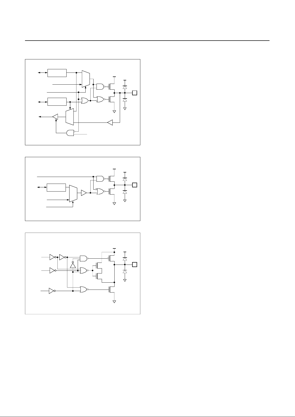
PORT STRUCTURES ..........................9
RESET................................................................ 9
TEST................................................................... 9
XIN, XOUT ........................................................9
OSC1, OSC2 ..................................................... 9
R00~07, R53 ...................................................... 9
R10~15 (AN0~5) ................................................ 9
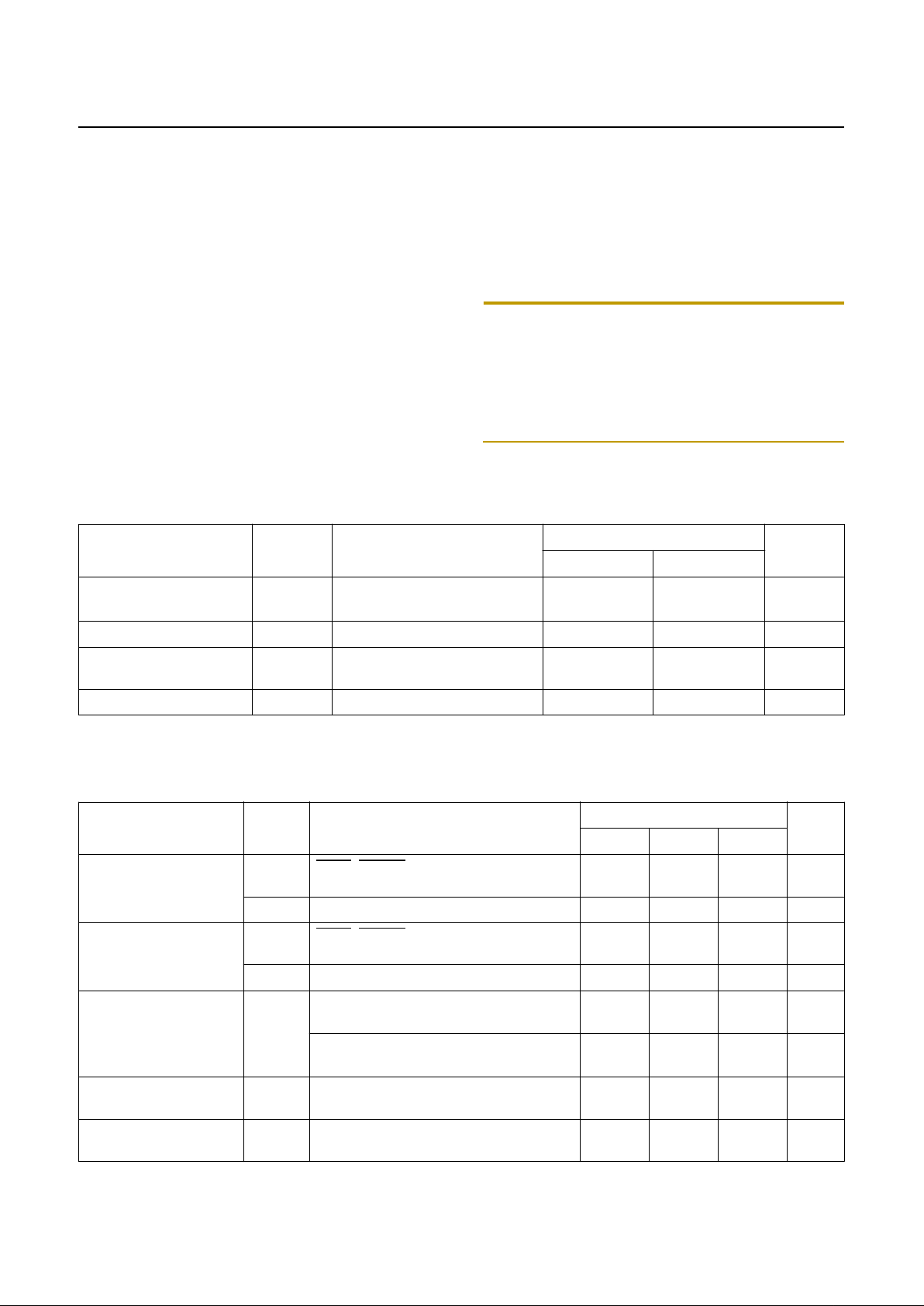
R16, 17, 20, 24, 25, 26, 27, 52, 67 ................... 10
R21/Sclk, R22/Sout .......................................... 10
R23/Sin ............................................................ 10
R40~43 (PWM0~3) .......................................... 10
R44, 45, 46, 47 (SCL, SDA, PWM) ..................10
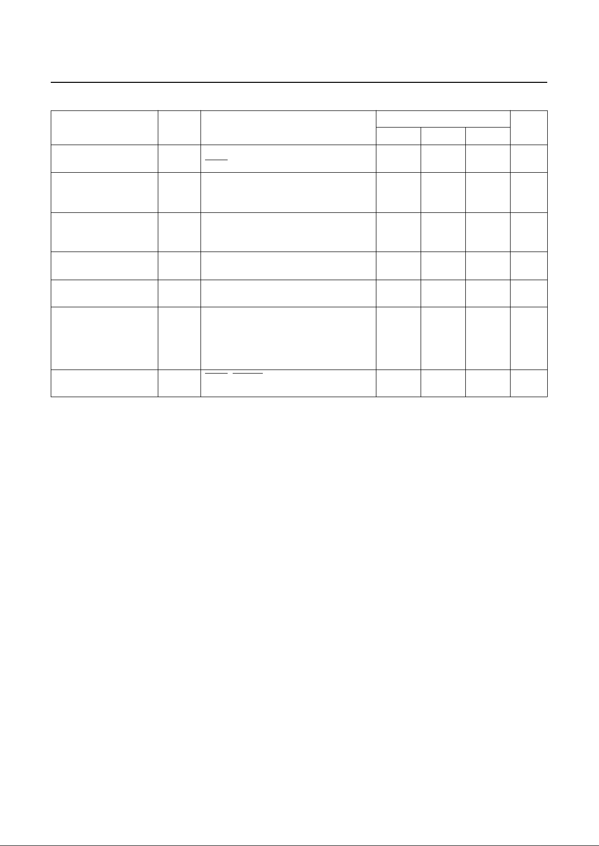
R50/BUZZ, R51/PWM8 ........ ......... ................. ..11
R54/YM, R55/YS, R56/I ...................................11
R, G, B ............................................................. 11
ELECTRICAL CHARACTERISTICS . 12
Absolute Maximum Ratings .....................12
Recommended Operating Conditions ....12
DC Electr i cal Characteristics - GM S81C404 0
.....................................................................12
A/D Comparator Characteristics .............14
AC Characteristics ....................................14
Typical Characteristics ............................16
MEMORY ORGANIZATION .............. 17
Registers ...................................................17
Program Memory ........ ............... .............. .20
PCALL→ rel ..................................................... 21
TCALL→ n ....................................................... 21
Data Memory ........ ............... .............. ........23
User Memory .................................................... 23
Control Registe rs ........................................... ..23
Stack Area ........................................................23
Addressing Mode ......................................25
(1) Register Addressing ...................................25
(2) Immediate Addressing → #imm .................. 25
(3) Direct Page Addressing → dp ....... .............. 25
(4) Absolute Addressing → !abs ....................... 25
(5) Indexed Addressing .................................... 26
X indexed direct page (no offset) → {X} ...........26
X indexed direct page, auto increment→ {X}+ . 26
X indexed direct page (8 bit offset) → dp+X .....26
Y indexed direct page (8 bit offset) → dp+Y .....27
Y indexed absolute → !abs+Y ..........................27
Direct page indirect → [dp] ...............................27
X indexed indirect → [dp+X] ............................. 27
Y indexed indirect → [dp]+Y ............................. 28
Absolute indirect → [!abs] ................................28
I/O PORTS ......................................... 29
Registers for Port .............. .............. .........29
Port Data Registers ..........................................29
I/O Ports Configuration ............................3 0
R0 Ports ...........................................................30
R1 Ports ...........................................................30
R2 Port .............................................................31
R4 Port .............................................................31
R5 Port .............................................................32
R6 Port .............................................................32
CLOCK GENERATOR ...................... 33
TIMER ................................................ 34
Basic Interval Timer .................................34
Timer 0, 1 ................. .............. ............... .....35
Timer / Event Counter 2, 3 ....... ............... .37
Timer Mode ...................................................... 39
Event counter Mode ......................................... 39
A/D Converter ................................... 42
Control ..............................................................42
Serial I/O ........................................... 44
Control ..............................................................44
Pulse Width Modulation (PWM) ...... 46
8bit PWM Control ............................................. 47
14bit PWM Control ........................................... 47
Interrupt interval measurement circuit
........................................................... 49
Control ..............................................................49
Buzzer driver .................................... 51
Control ..............................................................51
On Screen Display (OSD) ................ 53
OSDCON1 ....................................................... 55
OSDCON2 ....................................................... 55
OSDPOL .......................................................... 56
FDWSET .......................................................... 56
L1ATTR ............................................................ 57
L1VPOS ........................................................... 58
L2ATTR ............................................................ 58
L2VPOS ........................................................... 58
COLMOD ......................................................... 58
MESHCON ....................................................... 58
VRAM ...............................................................58
Font ROM .........................................................60
Page 4

GMS81C4040/87C4060
PRELIMINARY
2
PRELIMINARY
Nov. 1999 Ver 1.0
Sprite RAM ....................................................... 60
Test Font ..........................................................61
I2C Bus Interface ..............................62
Control .......... ................. ................ ................. ..62
I2C address register ......................................... 62
I2C data shift register [ICDR] ........................... 63
I2C status register ............................................63
I2C control register 1 ........................................ 64
I2C control register 2 ........................................ 64
START condition generation ............................ 65
RESTART condition generation ....................... 65
STOP condition generation .............................. 65
START / STOP condition detect ...................... 66
Address data communication ........................... 67
INTERRUPTS .................................... 68
Interrupt Mode Register ...................................68
Interrupt Sequence ......... .............. ............72
Interrupt acceptance ........................................72
Saving/Restoring General-purpose Register ... 73
Multi Interrupt ............................................74
External Interrupt .............. .............. .........75
Response Time ........... .......... ................ ........... 75
WATCHDOG TIMER ......................... 76
Watchdog Timer Control ..................................76
Enable and Disable Watchdog .........................77
Watchdog Timer Interrupt ................................77
Minimizing Current Consumption ..................... 78
OSCILLATOR CIRCUIT .................... 80
RESET ............................................... 81
External Reset Input ................. ............... .81
Watchdog Timer Reset ............................82
OTP Programming ........................... 83
GMS87C4060 OTP Programming ............83
.Device configuration data ......................84
Timing Chart .............................................87
Assemble mnemonics ..................... 89
Instruction Map ............................. ............89
Alphabetic order table of instruction .....90
Instruction Table by Function .................94
Page 5
PRELIMINARY
GMS81C4040/87C4060
Nov. 1999 Ver 1.0
PRELIMINARY
1
GMS81C4040/GMS87C4060
CMOS SINGLE-CHIP 8-BIT MICROCONTROLLER
FOR TELEVI SI ON
1. OVERVIEW
1.1 Description
The GMS81C4040/GMS87C4 060 is an adva nced CMOS 8-bi t micro control le r with 40K( 60K) bytes of ROM. T he device i s
one of GMS800 family. The HYUNDAI’s GMS81C4040/GMS87C4060 is a powerful microcontroller which provides a
highly flexible and cost effectiv e solution to many TV applications. The GMS81C4040/GMS87C4060 provides t he following standard features: 40K(60K) bytes of ROM, 1,536 bytes of RAM, 8-bit timer/counter .
1.2 Features
• 40K(60K) Bytes On-chip Program Memory
• 1,536 Bytes of On-chip Data RAM
(Included 256 bytes stack memory)
• Instruction Cycle Time (ex:NOP)
- 0.5us at 8MHz
• 40 Program m able I/O pins
- 33 I/O and 7 Outp ut pi ns
• Serial I/O : 8bit x 1ch
•I
2
C Bus interface
- Multimaster (2 Pairs interface pins)
• A/D Converter : 8bit x 6ch (TBD LSB)
• Pulse Width Modulation
- 14bit x 1ch
- 8bit x 6ch
•Timer
- Timer/Counter : 8bit x 4ch (16bit x 2ch)
- Basic interval timer : 8bit x 1ch
- Watch Dog Timer
• Number of Interrupt sources : 18
• On Screen Display
- Number of characters : 512 (6 characters are
reserved for IC test)
- Character size : 12 dots(X) x 16 dots(Y)
- Character display size : Large, Medium, Small
- DIsplay capability : 24Characters x 16 Line
(Two line VRAM buffer)
- Character, Back ground color : 16kinds
- Special functions : Rounding, Outline, Sprite,
Shadow,...
• Buzz er D riv in g port
- 500Hz ~ 250kHz @8MHz (Duty 50%)
• Operating Range : 4.5V to 5.5V
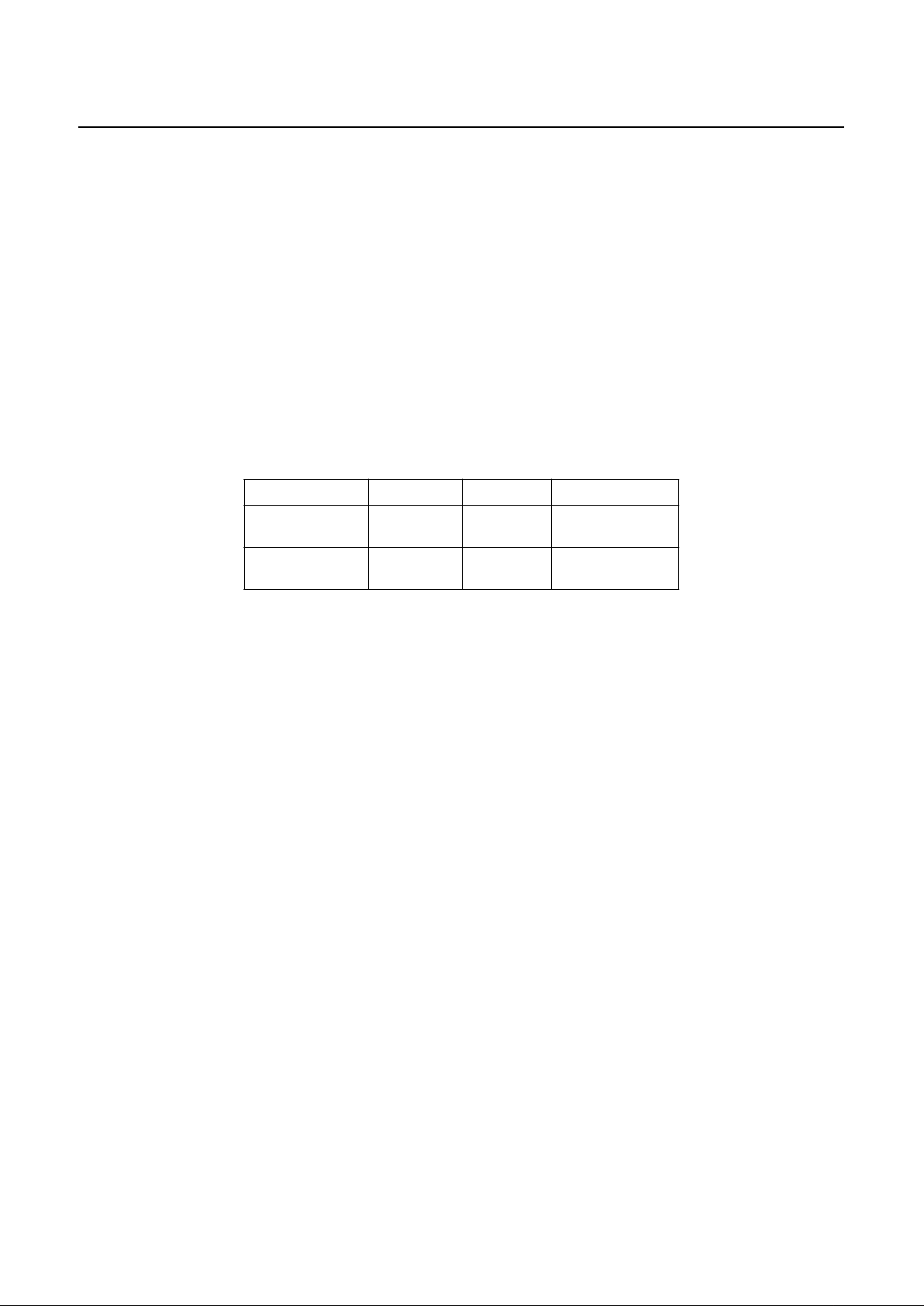
Device name ROM Size RAM Size Package
GMS81C4040
40K bytes
Mask ROM
1,536 bytes 52SDIP
GMS87C4060
60K bytes
EPROM
1,536 bytes 52SDIP
Page 6

GMS81C4040/87C4060
PRELIMINARY
2
PRELIMINARY
Nov. 1999 Ver 1.0
1.3 Development Tools
The GMS81C4040/GMS87C4060 is supported by a fullfeatured macro as sem bler / linker , OSD font editor, an incircuit emulator CHOICE-Dr
TM
.
In Circuit Emulators
CHOICE-Dr.
(with EVA81C4xxx board)
Assembler / Linker
HYUNDAI’s Macro Assembler /
Linker
Font Editor
MS-Windows GUI version
Debugger
MS-Windows GUI version
Page 7
PRELIMINARY
GMS81C4040/87C4060
Nov. 1999 Ver 1.0
PRELIMINARY
3
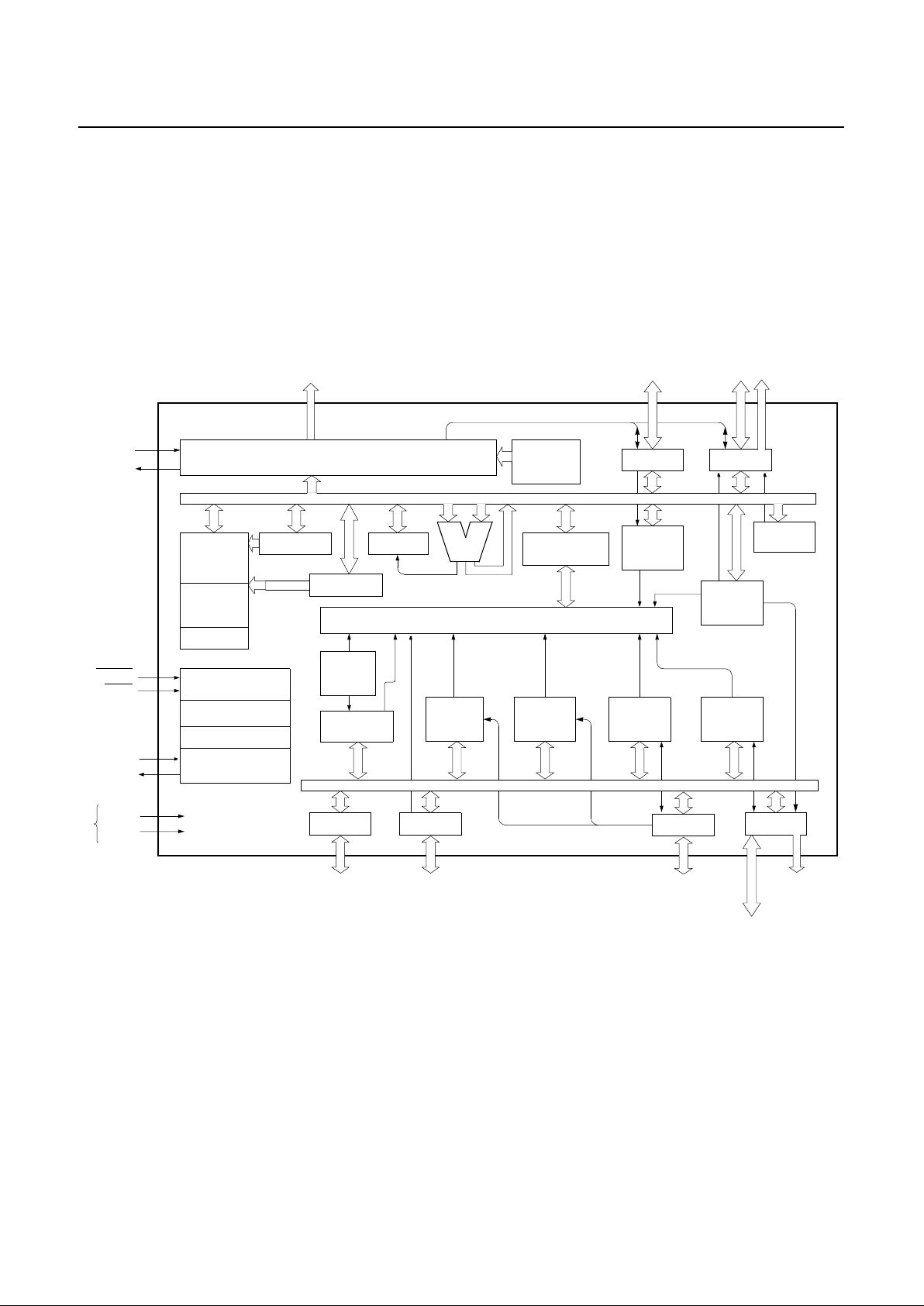
2. BLOCK DIAGRAM
ALU
OSD (On Screen Display) Controller
Accumulator
Interrupt Controller
Data
Memory
OSD
Memory
Display
8-bit x 4
Counter
Timer/
Program
Memory
Vector Table
8-bit Basic
Timer
Interval
Watchdog
Timer
PSW
System controller
Timing generator
System
Clock Controller
RESET
TEST
XIN
XOUT
OSC1
OSC2
R,G,B
VDD
VSS
Power
Supply
R1
Clock generator
& Index X,Y
8bit A/D
Convertor
Buzze r
R5
PWM
14bit x 1
8bit x 6
Da ta b u s
I2C
Interf a c e
R4
Da ta b u s
Serial I/O
Inte rfac e
Interrupt
Interv a l
Measure
R2
R0 R6
Stack pointer
PC
R00
R01
R02
R03
R04
R05
R06
R07
R67 / INT1
R20 / INT2
R21 / Sclk
R22 / Sout
R23 / Sin
R24 / INT3
R25 / EC2
R26 / INT4
R27 / EC3
R40 / PWM0
R41 / PWM1
R42 / PWM2
R43 / PWM3
R44 / SCL0
R45 / SCL1 / PWM4
R46 / SDA0
R47 / SDA1 / PWM5
R10 / AN0
R11 / AN1
R12 / AN2
R13 / AN3
R14 / AN4
R15 / AN5
R16 / VD
R17 / HD
R50 / BUZZ
R51 / PWM8
R52 / INT0
R53
R54 / YM
R55 / YS
R56 / I
Page 8
GMS81C4040/87C4060
PRELIMINARY
4
PRELIMINARY
Nov. 1999 Ver 1.0
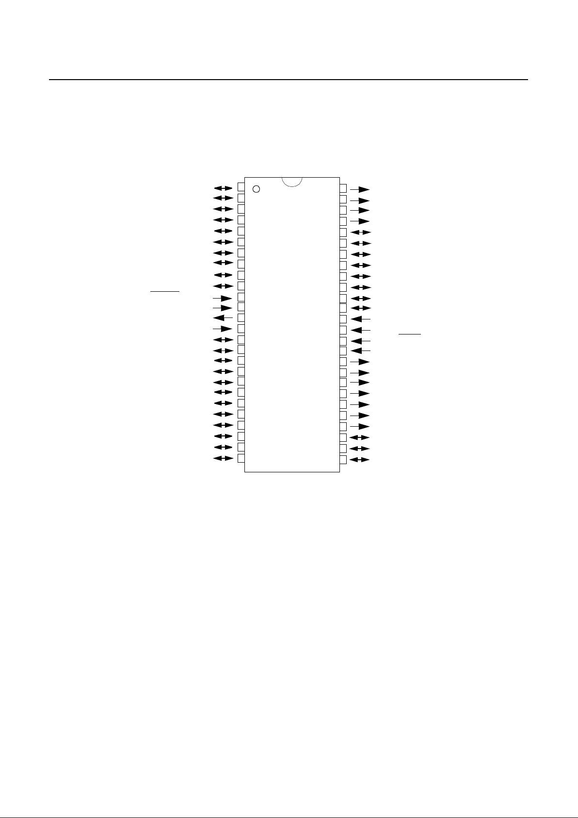
3. PIN ASSIGNMENT
R40/PWM0
R41/PWM1
R42/PWM2
R43/PWM3
R44/SCL0
R45/SCL1/PWM4
R46/SDA0
R47/SDA1/PWM5
R50/BUZZ
R51/PWM8
R52/INT0
R53
Vss
Vdd
TEST
OSC1
OSC2
R54/YM
R55/YS
R56/I
B
G
R
R00
R01
R02
R27/EC3
R26/INT4
R25/EC2
R24/INT3
R23/Sin
R22/Sout
R21/Sclk
R20/INT2
R17/HD
R16/VD
RESET
Vss
Xout
Xin
R15/AN5
R14/AN4
R13/AN3
R12/AN2
R11/AN1
R10/AN0
R07
R06
R05
R04
R03
R67/INT1
52
51
50
49
48
47
46
45
44
43
42
41
40
39
38
37
36
35
34
33
32
31
30
29
28
27
1
2
3
4
5
6
7
8
9
10
11
12
13
14
15
16
17
18
19
20
21
22
23
24
25
26
HYUNDAI
GMS81C40XX
Page 9
PRELIMINARY
GMS81C4040/87C4060
Nov. 1999 Ver 1.0
PRELIMINARY
5
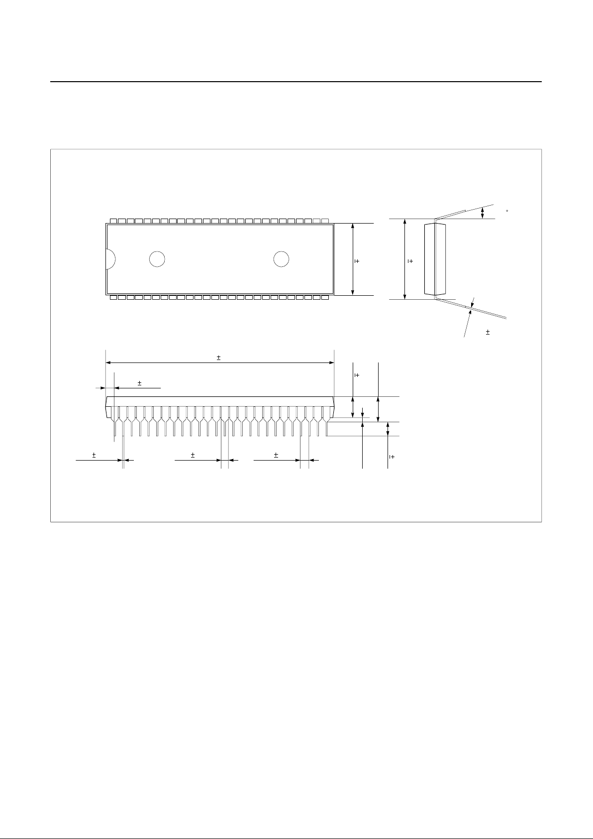
4. PACKAGE DIAGRAM
Figure 4-1 52pin Shrink DIP Package Diagram
UNIT: mm
HYUNDAI
GMS81C40XX
1
26
2752
45.97
0.13
0.76
0.13
1.778
0.25
4.38 Max.
13.97
0.25
15.24
0.25
0.47 0.13 1.02 0.25
3.81 0.13
3.24
0.20
0.50 Min.
0.25 0.05
0 ~ 15
Page 10

GMS81C4040/87C4060
PRELIMINARY
6
PRELIMINARY
Nov. 1999 Ver 1.0
5. PIN FUNCTION
V
DD
: Supply voltage.
V
SS
: Circuit ground.
TEST
: Used for shipping inspection of the IC. For normal
operation, it should not be connected .
RESET
: Rese t th e MCU.
X
IN
: Input to the inver tin g oscil lator ampli fie r and i nput to
the internal main clock operating circuit.
X
OUT
: Output from the inverting oscillator amplifier.
OSC1
: Input to the internal On Screen Display operating
circuit.
OSC2
: Output from the inverting OSC1 amplifier.
R00~R07
: R0 is an 8-bit CMOS bidi rec tional I/O port. R0
pins 1 or 0 written to the Port Direction Register can be
used as outputs or inpu ts.
R10~R17
: R1 is an 8-bit CMOS bidi rec tional I/O port. R1
pins 1 or 0 written to the Port Direction Register can be
used as outputs or inpu ts.
In addition, R1 serves the functions of the various following special features.
R20~R27
: R2 is a 8-bit CMOS bidi rectional I/O por t. Each
pins 1 or 0 written to the their Port Direction Register can
be used as outputs or inputs.
In addition, R2 serves the functions of the various following special features.
R40~R47
: R40~R43 are 8-bit NM OS open drain output
and R45~R47 are bidirec tional CMOS Input / NMOS open
drain output port. R4 pins 1 or 0 written to the Port Direction Registe r can be used as outputs or inputs .
In addition, R4 serves the functions of the various following sp ec ial featu r es.
R50~R56
: R50~R53 are 4-bi t CMOS bidire ctional I/ O and
R54~R56 are CMOS output port. R5 p ins 1 or 0 written to
the Port Direction Register can be used as outputs or inputs.
In addition, R5 serves the functions of the various following sp ec ial featu r es.
R67
: R67 is an 1- bit CMOS bidirection al I/O port. R67
pins 1 or 0 written to the Port Direction Register can be
used as outputs or inputs.
In addition, R67 serves the functions of the vario us following sp ec ial featu r es.
R,G,B
: R,G,B CMOS outpu t port. E ach pin s cont rols Re d,
Green,. Blue color co ntrol.
Port pin Alternate funct ion
R10
R11
R12
R13
R14
R15
R16
R17
AN0 (A/D converter input 0)
AN1 (A/D converter input 1)
AN2 (A/D converter input 2)
AN3 (A/D converter input 3)
AN4 (A/D converter input 4)
AN5 (A/D converter input 5)
VD (Vertical Sync. input)
HD (Horisontal Sync. input)
Port pin Alternate funct ion
R20
R21
R22
R23
R24
R25
R26
R27
INT2 (External interrupt input 2)
Sclk (Serial communication clock)
Sout (Serial communication data out)
Sin (Serial communi cation data in)
INT3 (External interrupt input 3)
EC2 (Event counter in put 2)
INT4 (External interrupt input 4)
EC3 (Event counter in put 3)
Port pin Alternate function
R40
R41
R42
R43
R44
R45
R46
R47
PWM0 (Pulse Width Modul ation output 0)
PWM1 (Pulse Width Modul ation output 1)
PWM2 (Pulse Width Modul ation output 2)
PWM3 (Pulse Width Modul ation output 3)
SCL0 (I
2
C Clock 0)
SCL1 (I
2
C Clock 1)
PWM4 (Pulse Width Modul ation output 4)
SDA0 (I
2
C Data 0)
SDA1 (I
2
C Data 1)
PWM5 (Pulse Width Modul ation output 5)
Port pin Alternate function
R50
R51
R52
R54
R55
R56
BUZZ (Buzzer output)
PWM8 (Pulse Width Modul ation output 8)
INT0 (External int errupt input 0)
YM (Back ground)
YS (Edge)
I (Intencity)
Port pin Alternate function
R67 INT1 (External int errupt input 1)
Page 11
PRELIMINARY
GMS81C4040/87C4060
Nov. 1999 Ver 1.0
PRELIMINARY
7
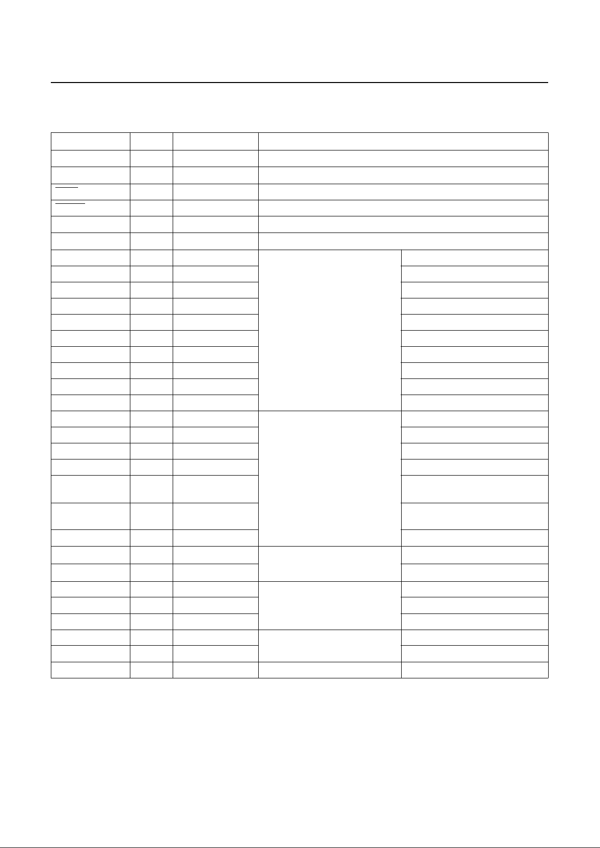
PIN NAME Pin No. In/Out Function
V
DD
39 - Supply voltage
V
SS
12, 40 - Circuit ground
TEST
38 I For test purposes. Should not be connected. (N.C.)
RESET
11 I Reset signal input
X
IN
14 I Main oscillation input
X
OUT
13 O Main oscillation output
OSC1 37 I
On screen display functions
On screen display oscillation input
OSC2 36 O On screen display osc. output
R17/HD 9 I/O Horisontal Sync. input
R16/VD 10 I/O Vertical Sync. input
R 30 O Red signal output
G 31 O Green signal output
B 32 O Blue signal output
R56/I 33 O Intencity sign al output
R55/YS 34 O Edge signal output
R54/YM 35 O Background signal output
R40/PWM0 52 O
PWM functions
8bit PWM
R41/PWM1 51 O 8bit PWM
R42/PWM2 50 O 8bit PWM
R43/PWM3 49 O 8bit PWM
R45/SCL1/
PWM4
47 I/O
Include I
2
C Serial clock 1 (SCL1)
R47/SDA1/
PWM5
45 I/O
Include I
2
C Serial data 1 (SDA1)
R51/PWM8 43 I/O 14bit PWM
R44/SCL0 48 I/O
I
2
C functions
I
2
C Serial clock 0
R46/SDA0 46 I/O
I
2
C Serial data 0
R23/Sin 5 I/O
SCI functions
Serial data input
R22/Sout 6 I/ O Ser ial data output
R21/Sclk 7 I/O Serial communication clock
R27/EC3 1 I/O
Timer event functions
Event counter input 3
R25/EC2 3 I/O Event counter input 2
R50/Buzzer 44 I /O Buzzer function 500Hz ~ 250KHz @8MHz
Table 5-1 Port Function Description
Page 12
GMS81C4040/87C4060
PRELIMINARY
8
PRELIMINARY
Nov. 1999 Ver 1.0
R52/INT0 42 I/O
External interrupt functions
External interrupt input 0
R67/INT1 26 I/O External interrupt input 1
R20/INT2 8 I/O External interrupt input 2
R24/INT3 4 I/O External interrupt input 3
R26/INT4 2 I/O External interrupt input 4
R10/AN0 20 I/O
A/D conversion functions
Analog input 0
R11/AN1 19 I/O Analog input 1
R12/AN2 18 I/O Analog input 2
R13/AN3 17 I/O Analog input 3
R14/AN4 16 I/O Analog input 4
R15/AN5 15 I/O Analog input 5
R00 29 I/O
Digital I/O functions
R01 28 I/O
R02 27 I/O
R03 25 I/O
R04 24 I/O
R05 23 I/O
R06 22 I/O
R07 21 I/O
R53 41 I/O
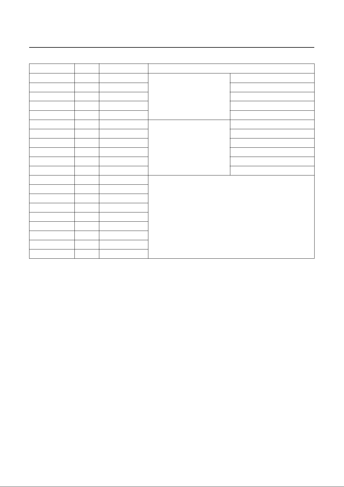
PIN NAME Pin No. In/Out Function
Table 5-1 Port Function Description
Page 13
PRELIMINARY
GMS81C4040/87C4060
Nov. 1999 Ver 1.0
PRELIMINARY
9
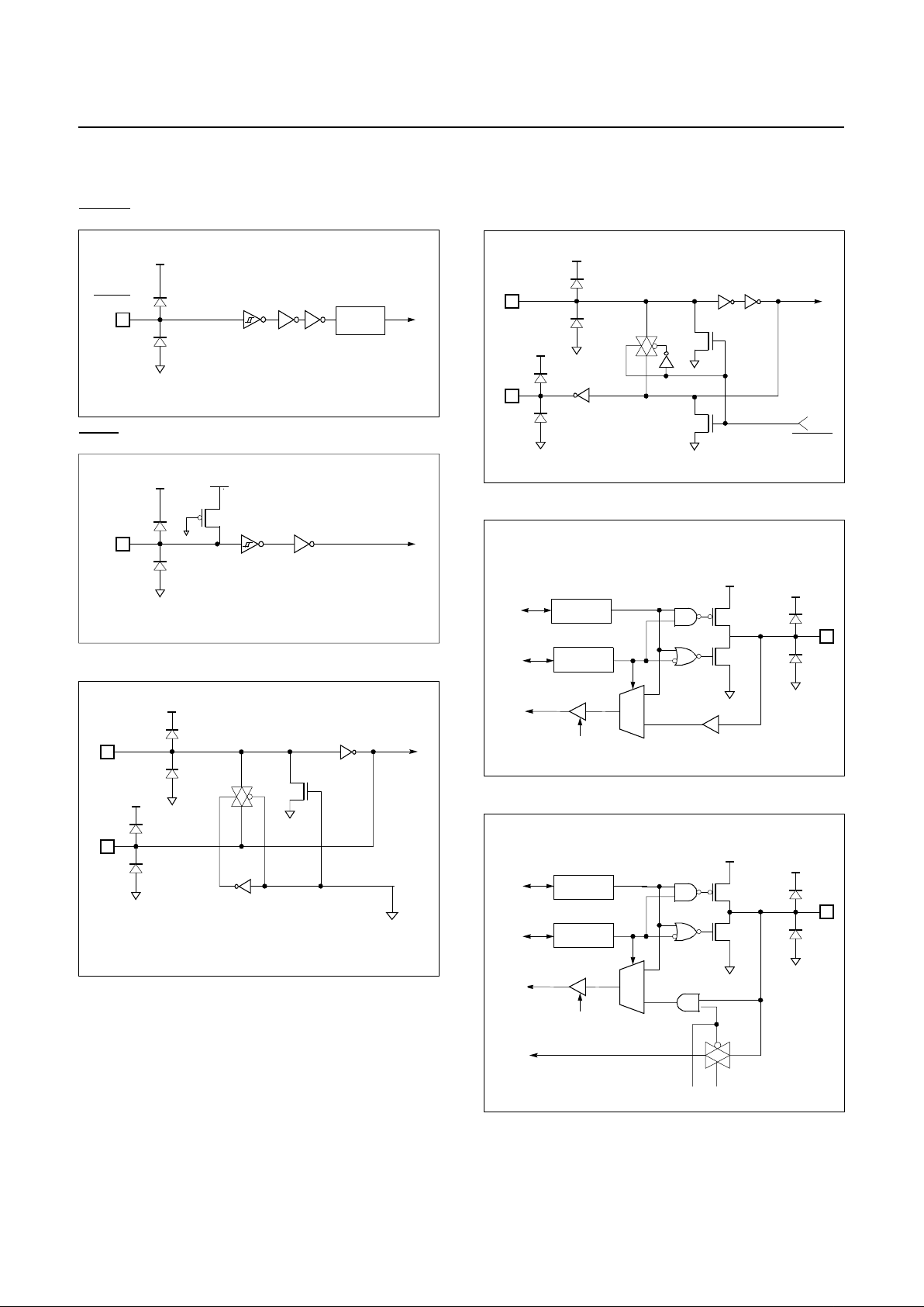
6. PORT STRUCTURES
RESET
TEST
XIN, X
OUT
OSC1, OSC2
R00~07, R53
R10~15 (AN0~5)
RESET
V
DD
V
SS
Noise
Canceler
V
DD
V
SS
X
IN
X
OUT
V
SS
V
DD
V
SS
V
DD
Main frequency
clock
V
SS
OSDON
OSC1
OSC2
V
SS
V
DD
V
SS
V
DD
Main frequency
clock
Pin
Data Reg.
Dir. Reg.
DB
DB
DB
MUX
RD
V
DD
V
SS
Pin
Data Reg.
Dir. Reg.
DB
DB
DB
MUX
RD
V
DD
V
SS
AN0~5
Page 14
GMS81C4040/87C4060
PRELIMINARY
10
PRELIMINARY
Nov. 1999 Ver 1.0
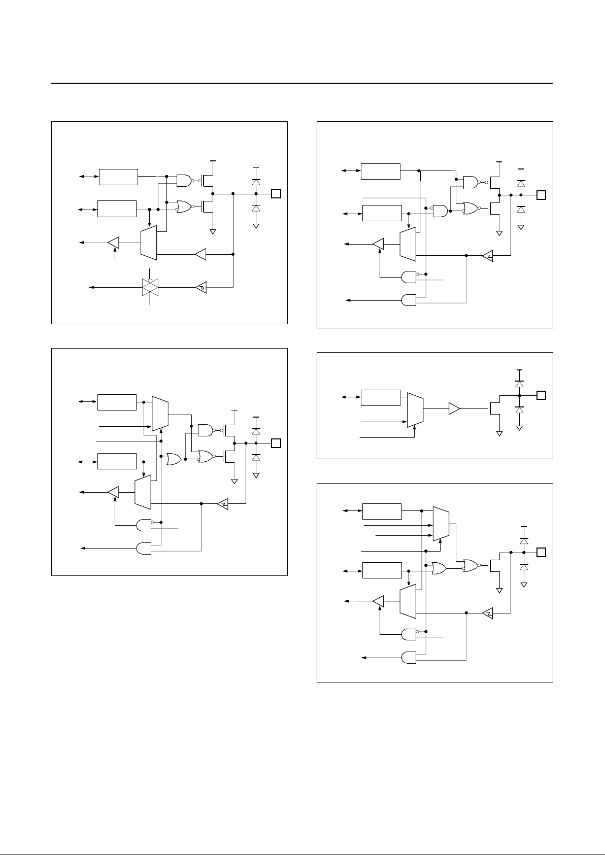
R16, 17, 20, 24, 25, 26, 27, 52, 67
R21/Sclk, R22/So ut
R23/Sin
R40~43 (PWM0~3)
R44, 45, 46, 47 (SCL, SDA, PWM)
Pin
Data Reg.
Dir. Reg.
DB
DB
DB
MUX
RD
V
DD
V
SS
HD,VD,
EC2~3
INT0~INT4
Pin
Data Reg.
Dir. Reg.
DB
DB
DB
MUX
RD
V
DD
V
SS
Sclk
MUX
Sout, Sclk
Selection
Pin
Data Reg.
Dir. Reg.
DB
DB
DB
MUX
RD
V
DD
V
SS
Sin
Selection
Pin
Data Reg.
DB
V
SS
MUX
PWM0~3
Selection
Pin
Data Reg.
Dir. Reg.
DB
DB
DB
MUX
RD
V
SS
SCL, SDA
MUX
PWM4,PWM5
Selection
SCL,SDA
Page 15
PRELIMINARY
GMS81C4040/87C4060
Nov. 1999 Ver 1.0
PRELIMINARY
11
R50/BUZZ, R51/PWM8
R54/YM, R55/YS, R56/I
R, G, B
Pin
Data Reg.
Dir. Reg.
DB
DB
DB
MUX
RD
V
DD
V
SS
MUX
Buzz, PWM8
Selection
Pin
Data Reg.
DB
V
DD
V
SS
MUX
YM, YS, I
Selection
OSD ON or Data Reg Write.
Pin
R, G, B
V
DD
V
SS
i
OSD_ON
Page 16
GMS81C4040/87C4060
PRELIMINARY
12
PRELIMINARY
Nov. 1999 Ver 1.0
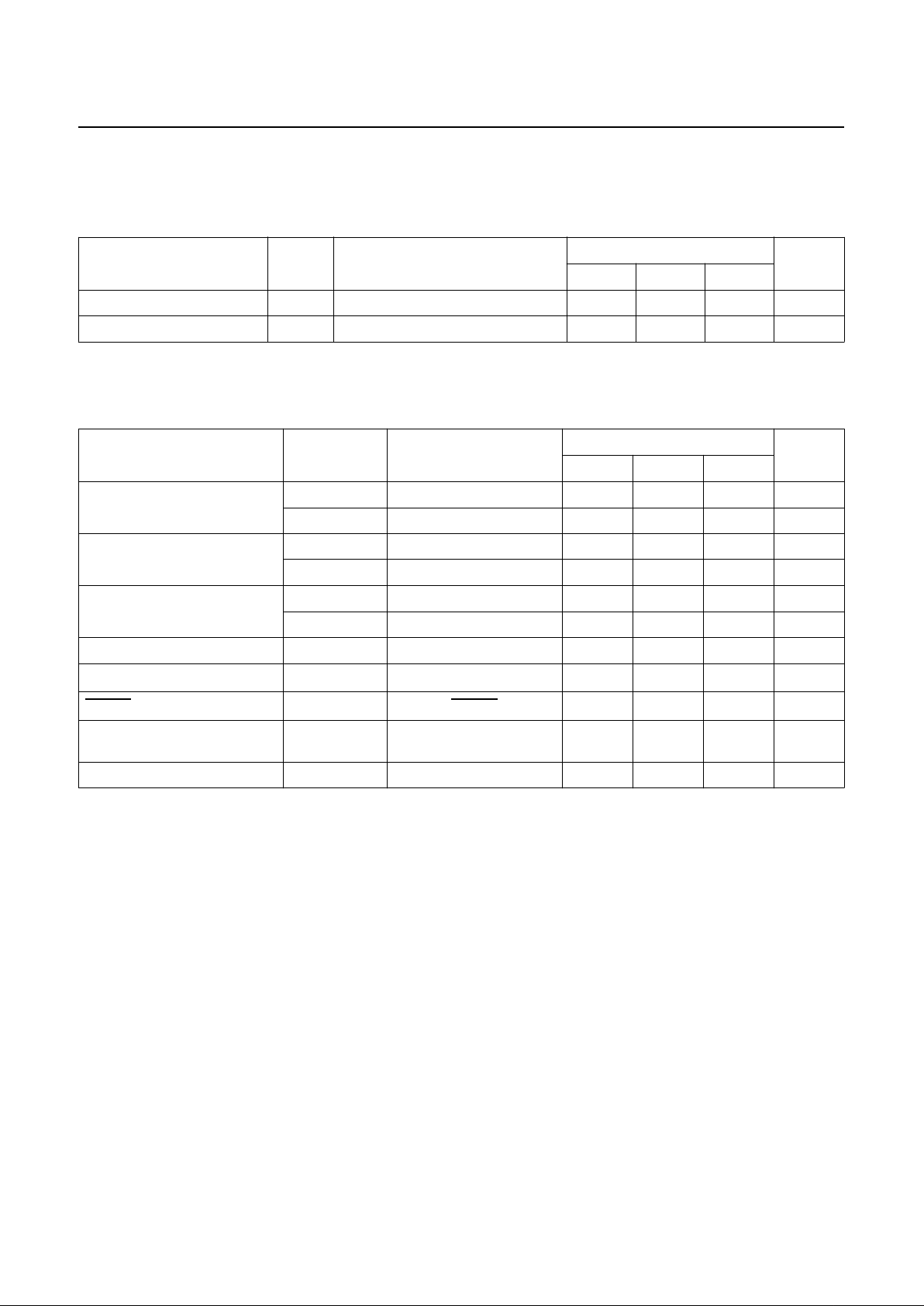
7. ELECTRICAL CHARACTERISTICS
7.1 Absolute Maximum Ratings
Supply voltage...........................................-0.3 to +6.0 V
Storage Temperature ................................-40 to +125 °C
Voltage on any pin with respect to Ground (V
SS
)
............................................................... -0.3 to V
DD
+0.3
Maximum current out of V
SS
pin ........................100 mA
Maximum current into V
DD
pin ............................80 mA
Maximum current sunk by (I
OL
per I/O Pin) ........20 mA
Maximum output current sourced by (I
OH
per I/O Pin)
...... .. .. .......................................................................8 mA
Maximum current (ΣI
OL
)......................................80 mA
Maximum current (ΣI
OH
)......................................50 mA
Note:
Stresses above those listed under "Absolute Maximum Ratings" may cause pe rmanent dam age to the device. This is a stress rating only and functional operation of
the device at a ny other conditio ns above those ind icated in
the operational sections of this specification is not implied.
Exposure to abso lute maximum rati ng conditions for extended periods may aff ect device reliability.
7.2 Recommended Operating Conditions
7.3 DC El ectrical Ch ar acteristi cs - GMS81C4040
(TA=-10~70°C, VDD=4.5~5.5V)
,
Parameter Symbol Condition
Specifications
Unit
Min. Max.
Supply Voltage
V
DD
f
XIN
=8MHz
f
OSC
=16MHz
4.5 5.5 V
Operating Frequency
f
XIN
VDD=4.5~5.5V
48MHz
On Screen Display Operating Frequency
f
OSC
VDD=4.5~5.5V
816MHz
Operating Temperature
T
OPR
-10 70
°
C
Parameter Symbol Condition
Specifications
Unit
Min. Typ. Max.
High level input vol tage
V
IH1
TEST, RESET, Xin, OSC1, R17~16,
R27~20, R47~44, R52, R67
0.8 V
DD
-
V
DD
V
V
IH2
R0, R15~10, R53~50
0.7 V
DD
-
V
DD
V
Low leve l in put vo lta g e
V
IL1
TEST, RESET, Xin, OSC1, R17~16,
R27~20, R47~44, R52, R67
0-
0.12 V
DD
V
V
IL2
R0, R15~10, R53~50 0 -
0.3 V
DD
V
High level output voltage
V
OH
I
OH
= -5mA
R0, R1, R2, R5, R67
V
DD
- 1
--V
I
OH
= -1.2mA
R,G,B
V
DD
- 1
--V
Low level output voltage
V
OL
I
OL
= 5mA
R0, R1, R2, R4, R5, R67, R, G, B
-
-1.0V
Supply current in
ACTIVE mode
I
DD
V
DD
--30mA
Page 17
PRELIMINARY
GMS81C4040/87C4060
Nov. 1999 Ver 1.0
PRELIMINARY
13
pull-up lekage current
I
RUP
VDD = 5.5v, V
PIN
= 0.4V
TEST
-1.5 -400
µ
A
High input leakage
current
I
IZH
V
DD
= 5.5V, V
PIN
= V
DD
All input, I/O pin s except XIN, OSC1,
R47~40
-5 - 5
µ
A
Low input leakage
current
I
IZL
V
DD
= 5.5V, V
PIN
= 0V
All input, I/O pin s except X
IN
, OSC1,
R47~44
-5 - 5
µ
A
Open drain leakage
current
I
LOZ
V
DD
= 5.5V, V
OH
= VDD, N-ch Tr. off
R47~40
--10µA
RAM data retention
voltage
V
RAMVDD
1.2 - - V
I
2
C port impedance
(I/O Tra n s is to r o ff)
R
BS
V
DD
= 4.5V
,
V
SCL0
= V
SCL1
= 2.25V
V
SDA0
= V
SDA1
= 2.25V
SCL0:SCl1 (R44:R45)
SDA0:SDA1 (R46:R47)
- - 120
Ω
Hysterisis
Vt+ ~
Vt-
TEST
, RESET, Xin, OSC1, R17~16,
R27~20, R47~44, R52, R67
1.0 - - V
Parameter Symbol Condition
Specifications
Unit
Min. Typ. Max.
Page 18
GMS81C4040/87C4060
PRELIMINARY
14
PRELIMINARY
Nov. 1999 Ver 1.0
7.4 A/D Comparator Characteristics
(TA=-10~70°C, VDD=5.0V)
7.5 AC Characteristics
(TA=-10~70°C, VDD=5V±10%, VSS=0V)
Parameter Symbol Pins
Specifications
Unit
Min. Typ. Max.
Analog Input Voltage Range
V
AIN
AN0~AN5
V
SS
-
V
DD
V
Accuracy
N
FS
---
ΤΒ∆
LSB
Parameter Symbol Pins
Specifications
Unit
Min. Typ. Max.
Operating Frequency
f
XIN
X
IN
4-8MHz
f
OSC
OSC 8 - 16 MHz
External Clock Pulse Width
t
MCPW
X
IN
62.5 - 125 nS
t
SCPW
S
CLK
0.5 -
µ
S
External Clock Transition Time
t
MRCP,tMFCP
X
IN
- - 20 nS
t
SRCP,tSFCP
S
CLK
- - 20 nS
Oscillation Stabilizing Time
t
ST
XIN, X
OUT
--20mS
Interrupt Pulse Width
t
IW
INT0~4 2 - -
t
SYS
1
RESET Inpu t Width
t
RST
RESET 8--
t
SYS
1
Event Counter Input Pulse
Width
t
ECW
EC2, EC3 2 - -
t
SYS
1
Event Counter Transition Time
t
REC,tFEC
EC2, EC3 - - 20 nS
1. t
SYS
is one of 2/f
XIN
main cloc k operation mode,
Page 19
PRELIMINARY
GMS81C4040/87C4060
Nov. 1999 Ver 1.0
PRELIMINARY
15
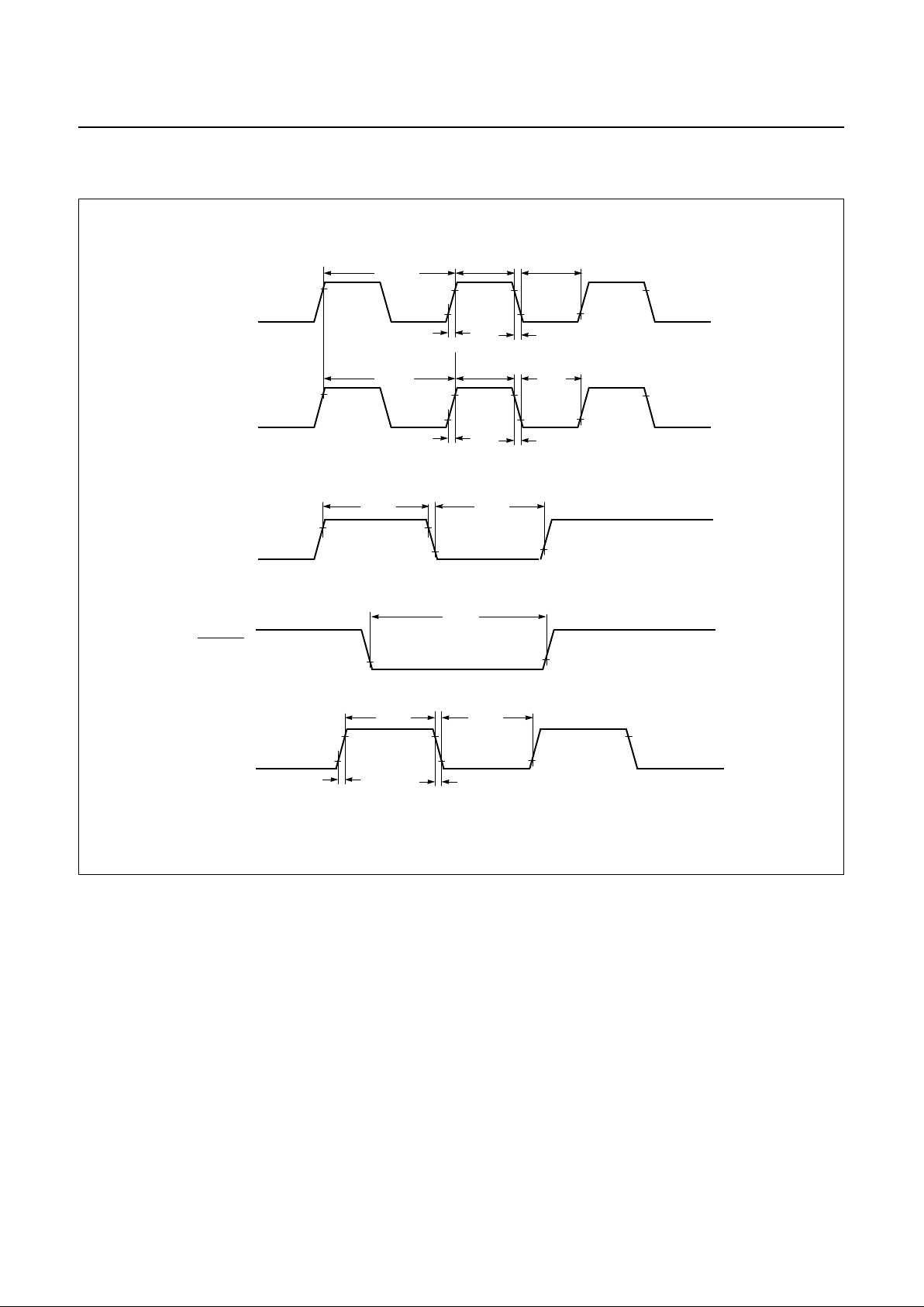
Figure 7-1 Timing Chart
t
MRCP
t
MFCP
X
IN
INT0 ~ 4
0.5V
V
DD
-0.5V
0.2V
DD
0.8V
DD
0.2V
DD
RESET
t
REC
t
FEC
0.2V
DD
0.8V
DD
EC2, EC3
t
IW
t
IW
t
RST
t
ECW
t
ECW
1/f
XIN
t
MCPW
t
MCPW
t
SRCP
t
SFCP
S
CLK
0.5V
V
DD
-0.5V
1/f
SCLK
t
SCPW
t
SCPW
Page 20

GMS81C4040/87C4060
PRELIMINARY
16
PRELIMINARY
Nov. 1999 Ver 1.0
7.6 Typical Characteristics
This data will generate after evaluation.
Not available at this time.
Page 21
PRELIMINARY
GMS81C4040/87C4060
Nov. 1999 Ver 1.0
PRELIMINARY
17
8. MEMORY ORGANIZATION
The GMS81C4040/GMS87C4060 has separate address
spaces for P rogram memo ry, Data M emory and D isplay
memory. Program memory can only be read, not written
to. It can be up to 40K/60K byte s of Program memo ry.
Data memory can be read and written to up to 1,536 bytes
including the stack area. Font memory has prepared 16K
bytes for OSD.
8.1 Registers
This device has six registers that are the Program Counter
(PC), a Accumulator (A), two index registers (X, Y), the
Stack Pointer (SP), and the Program Status Word (PSW).
The Program Counter consists of 16-bit register .
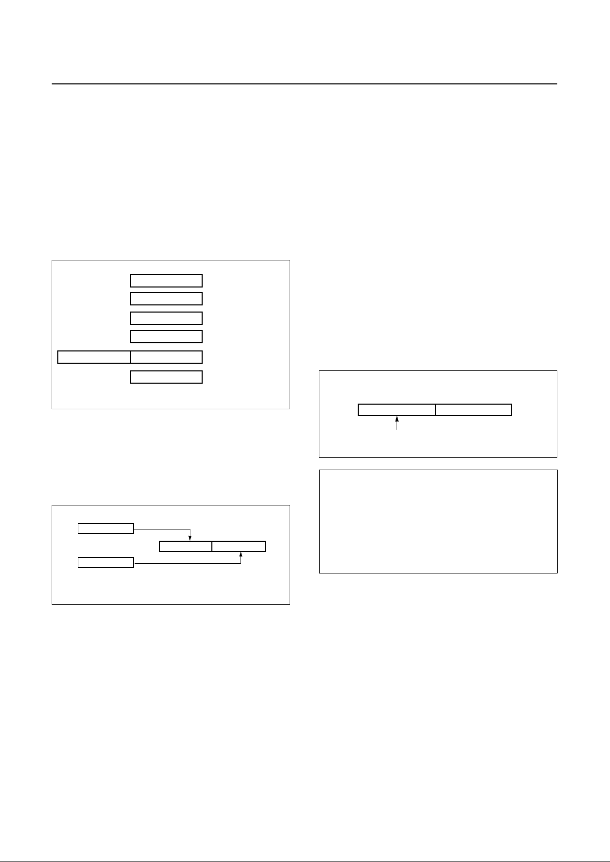
Figure 8-1 Configuration of Registers
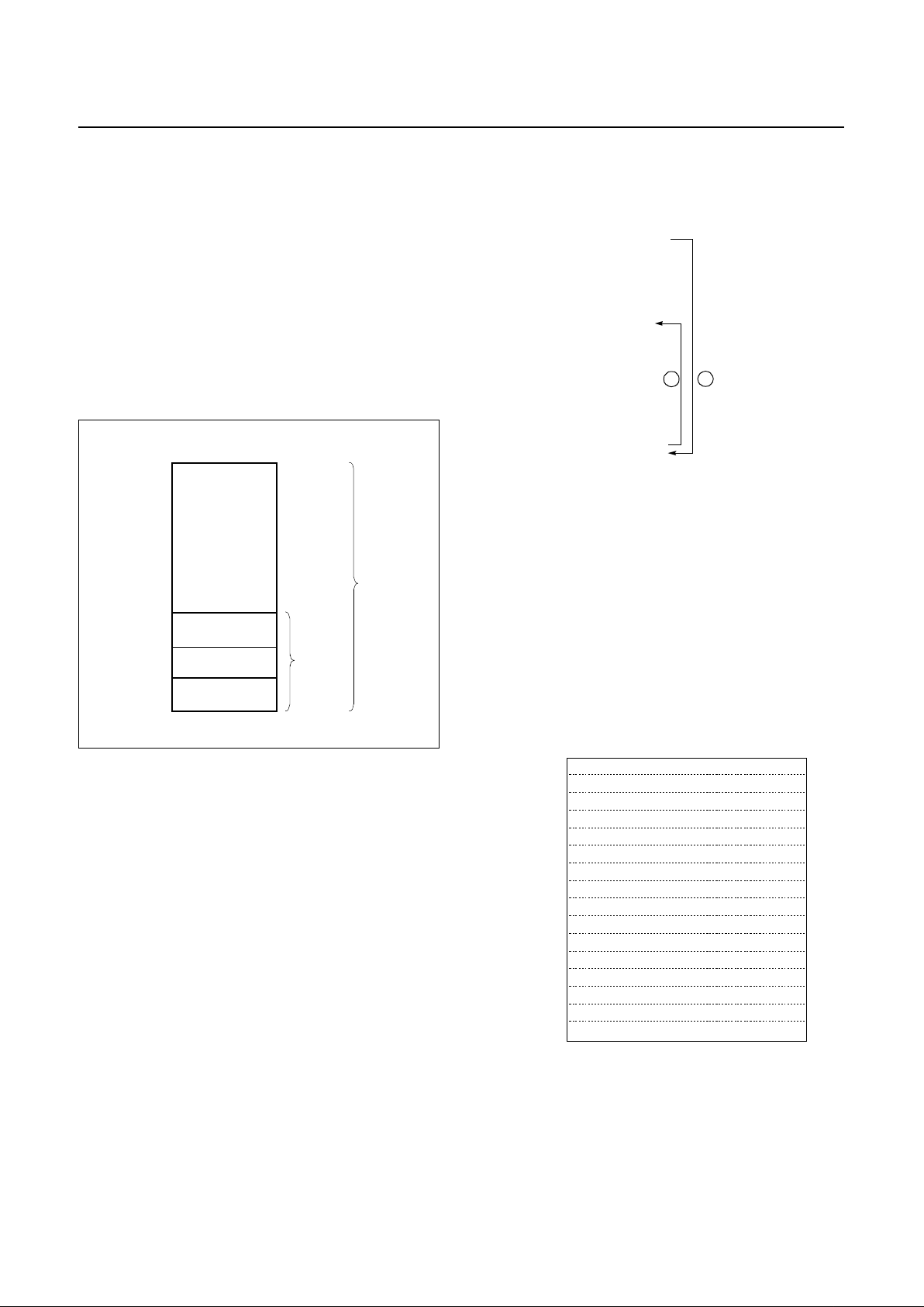
Accumulator:
The Accumulator is the 8-bit general purpose register, use d for data opera tio n such as tr ansfer , temporary saving, an d conditional judgement, etc.
The Accumulator can be used as a 16-bit register with Y
Register as shown below.
Figure 8-2 Configurati on of YA 16-bit Register
X, Y Registers
: In the addressing mode which uses these
index registers , the regist er contents are a dded to the specified addr ess, which be comes the act ual address. The se
modes are extremely effective for referencing subroutine
tables and memory table s. The index re gisters al so have increment, decrement, comparison and data transfer functions, and they can be used as simple accumulators.
Stack Pointer
: The Sta ck Poi nte r is an 8-b it re gist er us ed
for occurrence inte rrupts and calling ou t subrouti nes. Stack
Pointer identifies the location in the stack to be accessed
(save or restor e).
Generally, SP is automatically updated when a subroutine
call is executed or an interrupt is accepted. However, if it
is used in excess of the stack area permitted by the data
memory allocating configuration, the user-processed data
may be lost.
The stack can be located at any position within 0100
H
to
01FF
H
of the internal data memory. The SP is not initialized by hardware, requiring to write the initial value (the
location wit h whi ch the use of the stac k st arts) by u sing t he
initialization routine. Normally, the initial value of "FF
H
"
is used.
Program Counter
: The Program Counter is a 16-bit wi de
which consists of two 8-bit registers, PCH and PCL. This
counter indicates the address of the next instruction to be
executed. In reset state, the pr o g ram cou n ter has r eset routine address (PC
H
:0FFH, PCL:0FEH).
Program Status Word
: The Program Status Word (PSW)
contains several bits that reflect the current state of the
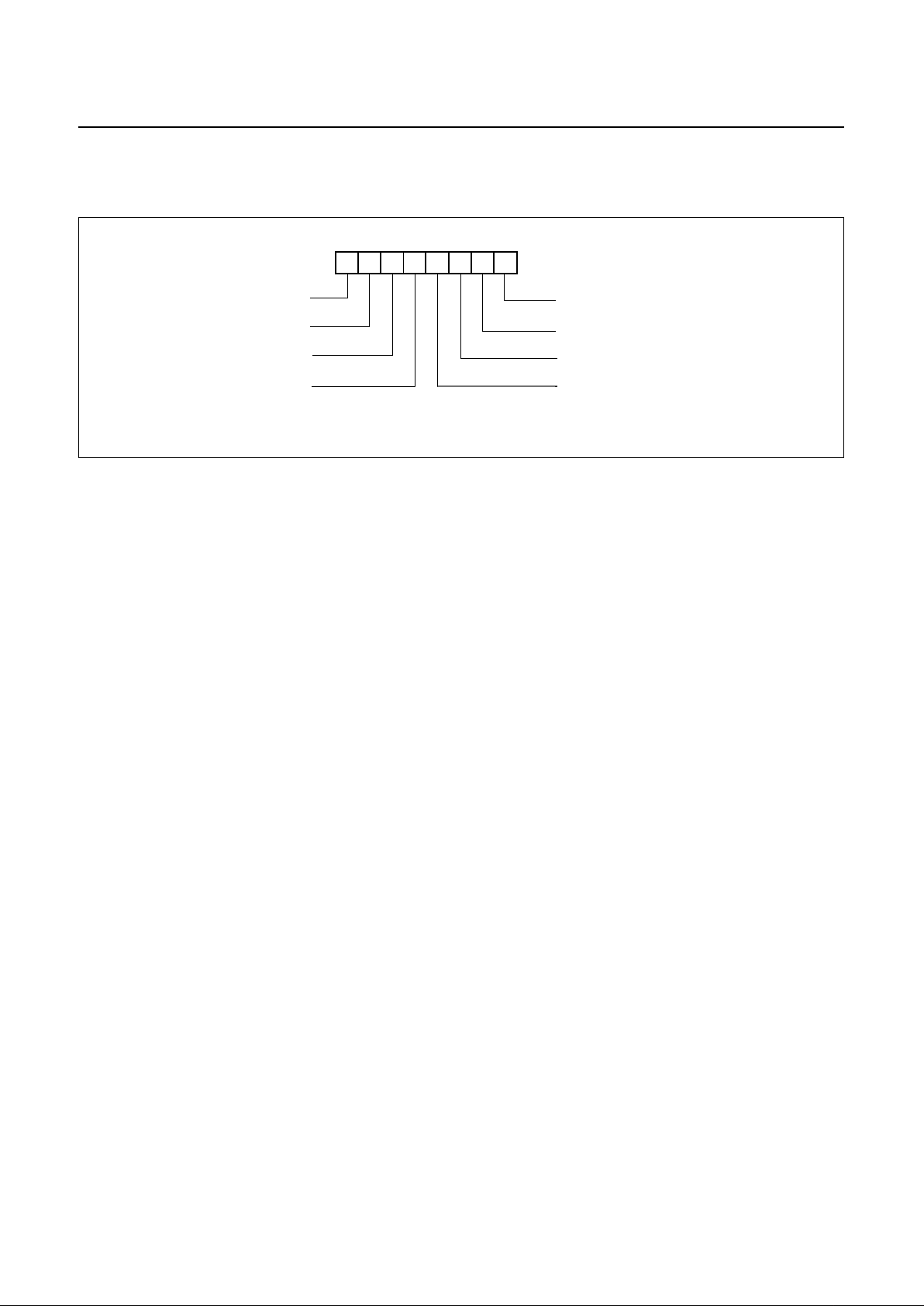
CPU. The PSW is described in Figure 8-3 . It contains the
Negative flag, the Overflow flag, the Break flag the Half
Carry (for BCD operation), the Interrupt enable flag, the
Zero flag, and the Carry flag.
[Carry flag C]
This flag stores a ny carry o r borro w from the ALU of CPU
A
ACCUMULATOR
X REGISTER
Y REGISTER
STACK PO INT ER
PROGRAM COUNTER
PROGRAM STATUS
WORD
X
Y
SP
PCLPCH
PSW
Two 8-bit Registers can be used as a "YA" 16-bit Register
Y
A
Y A
Caution:
The Stack Pointer must be initialized by software be-
cause its value is un d ef ined aft er RESET.
Example: To initialize the SP
LDX #0FFH
TXSP ; SP ← FF
H
SP
01
Stack Address ( 0100
H
~ 01FFH )
15 087
Hardware fixed
Page 22
GMS81C4040/87C4060
PRELIMINARY
18
PRELIMINARY
Nov. 1999 Ver 1.0
after an arithmetic operation and is also changed by the
Shift Instruction or Rotate Instruction.
Figure 8-3 PSW (Program Status Wo rd) Register
[Zero flag Z]
This fl ag is set when the re sult of an arith metic op erat ion
or data transfer is "0" and is cleared by any other result.
[Interrupt disable flag I]
This flag enables/disables all interrupts except interrupt
caused by Reset o r software BRK in struction. All interrupts are disabled when cleared to "0". This flag immediately becomes "0" when an interrupt is served. It is set by
the EI instruction and cleared by the DI instruction.
[Half carry flag H]
After operation, this is set when there is a carry from bit 3
of ALU or there is borrow from bit 4 of ALU. This bit can
not be set or cleared except CLRV instruction with Overflow flag (V).
[Break flag B]
This flag is set by software BRK instruct ion to distinguish
BRK from TCA LL instruction with the s ame vector address.
[Direct page flag G]
This flag a ssigns RAM pa ge for dire ct a ddres sing mode. In
the direct addressing mode, addressing area is from zero
page 00
H
to 0FFH when this flag is "0". If it is set to "1",
addressing area is assigned by DPGR register (address
0F8
H
). It is set by SETG i nstru ction a nd clear ed by CL RG.
[Overflow flag V]
This flag is set to "1" when an overflow occurs as the result
of an arithmetic operation involving signs. An overflow
occurs when the r esult of an add ition or s ubtraction exceeds + 127(7F
H
) or -128(80H). The CLRV instruction
clears the overflow flag. There is no set instruction. When
the BIT instruction is executed, bit 6 of memory is copied
to this flag.
[Nega tiv e f la g N ]
This flag is set to match the sign bit (bit 7) status of the re-
sult of a data or arithmetic operation. When the BIT instruction is execu ted, bit 7 of memor y is copied to this fla g.
N
NEGATIVE FLAG
V G B H I Z C
MSB LSB
RESET VALUE : 00
H
PSW
OVERFLOW FLAG
BRK FLAG
CARRY FLAG RECEIVES
ZERO FLAG
INTERRUPT ENABLE FLAG
CARRY OUT
HALF CARRY FLAG RECEIVES
CARRY OUT FROM BIT 1 OF
ADDITION OPERLANDS
SELECT DIRECT PAGE
when G=1, page is addressed by RPR
Page 23
PRELIMINARY
GMS81C4040/87C4060
Nov. 1999 Ver 1.0
PRELIMINARY
19
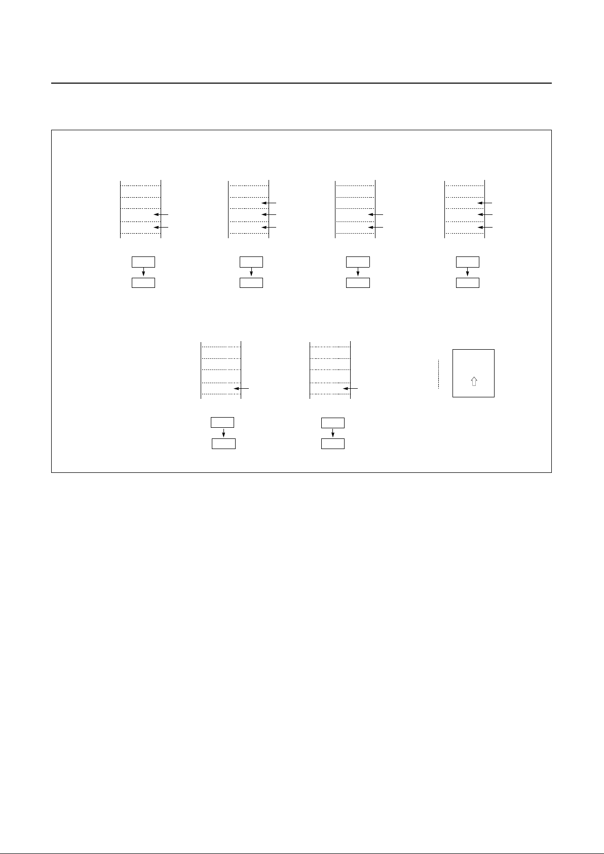
Figure 8-4 Stack Operation
At execution of
a CALL/TCALL/PCALL
PCL
PCH
01FF
SP after
execution
SP before
execution
01FD
01FE
01FD
01FC
01FF
Push
down
At acceptance
of interrupt
PCL
PCH
01FF
01FC
01FE
01FD
01FC
01FF
Push
down
PSW
At execution
of RET instruction
PCL
PCH
01FF
01FF
01FE
01FD
01FC
01FD
Pop
up
At execution
of RETI instruction
PCL
PCH
01FF
01FF
01FE
01FD
01FC
01FC
Pop
up
PSW
0100H
01FFH
Stack
depth
At execution
of PUSH in struction
A
01FF
01FE
01FE
01FD
01FC
01FF
Push
down
SP after
execution
SP before
execution
PUSH A (X,Y,PSW)
At execution
of POP instruction
A
01FF
01FF
01FE
01FD
01FC
01FE
Pop
up
POP A (X,Y,PSW)
Page 24
GMS81C4040/87C4060
PRELIMINARY
20
PRELIMINARY
Nov. 1999 Ver 1.0
8.2 Program Memory
A 16-bit program counter is capable of addressing up to
64K bytes, but GMS81C4040/GMS87C4060 has 40K/
60K bytes program memory space only physically implemented. Accessing a location above FFFF
H
will cause a
wrap-around to 0000
H
.
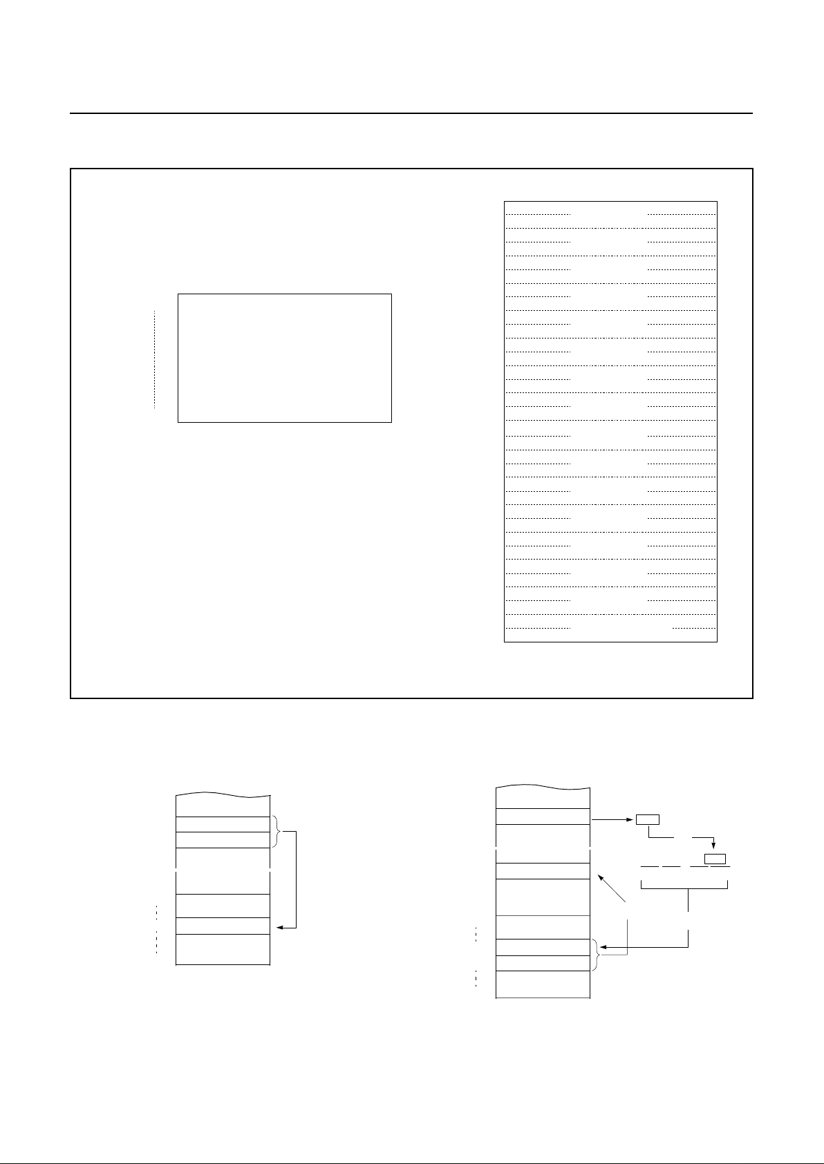
Figure 8-5 , shows a map of Pro gram Memory. Aft er reset,
the CPU begins e xecution from reset vect or which is stored
in address FFFE
H
and FFFFH as shown in Figure 8-6 .
As shown in Figure 8-5 , each area is assigned a fixed location in Program Memory. Progr am Memory area c ontains the user program.
Figure 8-5 Program Memory Map
Page Call (PCALL) area contains subroutine program to
reduce program byte length by using 2 bytes PCALL instead of 3 bytes CALL instr uction. If it is frequent ly called ,
it is more useful to save program byte length.
Table Call (TCALL) causes the CPU to jump to each
TCALL address, where it commences the execution of the
serv ic e r ou t in e. Th e Tab l e Call servic e area space s 2 - b y te
for every TCALL: 0FFC0
H
for TCALL15, 0FFC2H for
TCALL14, etc., as shown in Figure 8-7 .
Example: Usage of TCALL
The in terrup t cau s es the CP U to ju m p to s p ec if ic loca t i on ,
where it comm ence s the ex ecuti on of th e serv ice ro utine.
The External interrupt 0, for example, is assigned to location 0FFFC
H
. The in terr up t se rvic e lo catio ns spa ces 2-by te
interval: 0FFF8
H
and 0FFF9H for Ex terna l Interr upt 1,
0FFFC
H
and 0FFFDH for External Interrupt 0, etc.
Any area from 0FF00
H
to 0FF FFH, if it is not going to be
used, its service location is available as general purpose
Program Memory.
Figure 8-6 Interr upt Vector Area
PROGRAM
MEMORY
TCALL
AREA
INTERRUPT
VECTOR AREA
81C4040:6000H
FEFFH
FF00H
FFC0H
FFDFH
FFE0H
FFFFH
PCALL
AREA
81C4060:1000H
FFBFH
LDA #5
TCALL 0FH ;
1BYTE INSTRUCTION
:;
INSTEAD OF 2 BYTES
:;
NORMAL CALL
;
;TABLE CALL ROUTINE
;
FUNC_A: LDA LRG0
RET
;
FUNC_B: LDA LRG1
RET
;
;TABLE CALL ADD. AREA
;
ORG 0FFC0H ;
TCALL ADDRESS AREA
DW FUNC_A
DW FUNC_B
1
2
0FFE0
H
E2
Address Vector Area Memory
E4
E6
E8
EA
EC
EE
F0
F2
F4
F6
F8
FA
FC
FE
I
2
C Bus Interface Interrupt Vector Area
Serial I/O Interrupt Vector Area
Basic Interval Timer Interrupt Vector Area
Watchdog Timer Interrupt Vector Area
Timer/Counter 3 Interrupt Vector Area
Timer/Counter 1 Interrupt Vector Area
V-Sync Interrupt Vector Area
Timer/Counter 2 Interrupt Vector Area
Timer/Counter 0 Interrupt Vector Area
External Interrupt 2 Vector Area
On Screen Display Interrupt Vector Area
External Interrupt 0 Vector Area
RESET Vector Area
External Interrupt 1 Vector Area
1 Frame Timer Interrupt Vector Area
External Interrupt 3/4 Vector Area
"-" means reserved area.
NOTE:
Page 25
PRELIMINARY
GMS81C4040/87C4060
Nov. 1999 Ver 1.0
PRELIMINARY
21
Figure 8-7 PCALL and TCALL Memory Area
PCALL→
→ →
→ rel
4F35 PCALL 35H
TCALL →
→ →
→ n
4A TCALL 4
0FFC0
H
C1
Address Program Memory
C2
C3
C4
C5
C6
C7
C8
0FF00
H
Address PCALL Area Memory
0FFBF
H
PCALL Area
(192 Bytes)
* means that the BRK software interrupt is using
same address with TCALL0.
NOTE:
TCALL 15
TCALL 14
TCALL 13
TCALL 12
TCALL 11
TCALL 10
TCALL 9
TCALL 8
TCALL 7
TCALL 6
TCALL 5
TCALL 4
TCALL 3
TCALL 2
TCALL 1
TCALL 0 / BRK *
C9
CA
CB
CC
CD
CE
CF
D0
D1
D2
D3
D4
D5
D6
D7
D8
D9
DA
DB
DC
DD
DE
DF
4F
~
~
~
~
Sub-routine
35
0FF35H
0FF00H
0FFFFH
Upper address is
assumed 0FF
H.
11111111
11010110
01001010
PC:
FHFHDH6
H
4A
~
~
~
~
25
0FFD6H
0FF00H
0FFFFH
D1
Sub-routine
0FFD7H
þ
À
Ã
0D125H
Reverse
Page 26

GMS81C4040/87C4060
PRELIMINARY
22
PRELIMINARY
Nov. 1999 Ver 1.0
Example: The usage software example of Vector address and the initialize part.
ORG 0FFE0H
DW I2C ; I2C
DW SERIAL ; Serial I/ O
DW BIT ; Basic interval timer
DW WATCHDOG ; Watch dog timer
DW INT3_4 ; Interrupt 3/4
DW TIMER3 ; Timer 3
DW TIMER1 ; Timer 1
DW VSYNC ; Vertica l Sy nc .
DW One_Frame ; 1 Frame interrupt
DW TIMER2 ; Timer 2
DW TIMER0 ; Timer 0
DW INT2 ; Interrupt 2
DW INT1 ; Interrupt 1
DW OSD ; On Screen Display
DW INT0 ; Interrupt 0
DW RESET ; Reset
ORG 0F000H
;****** ** ** ** ****** ** *** ** ** ************* ** **
; MAIN PROGRAM *
;********************************************
;
RESET: DI ; Disable All Interrupts
LDX #0
LDA #0 ; RAM Clear(!0000H->!00BFH)
RAM_CLR: STA {X}+
CMPX #0C0H
BNE RAM_CLR
;
CALL LCD_CLR ; Clear LCD display memory
;
LDX #03FH ; Stack Pointer Initialize
TXSP
LDM R0, #0 ; Normal Port 0
LDM R0DD,#1000_0010B ; Normal Port Direction
:
:
:
:
Page 27
PRELIMINARY
GMS81C4040/87C4060
Nov. 1999 Ver 1.0
PRELIMINARY
23
8.3 Data Memory
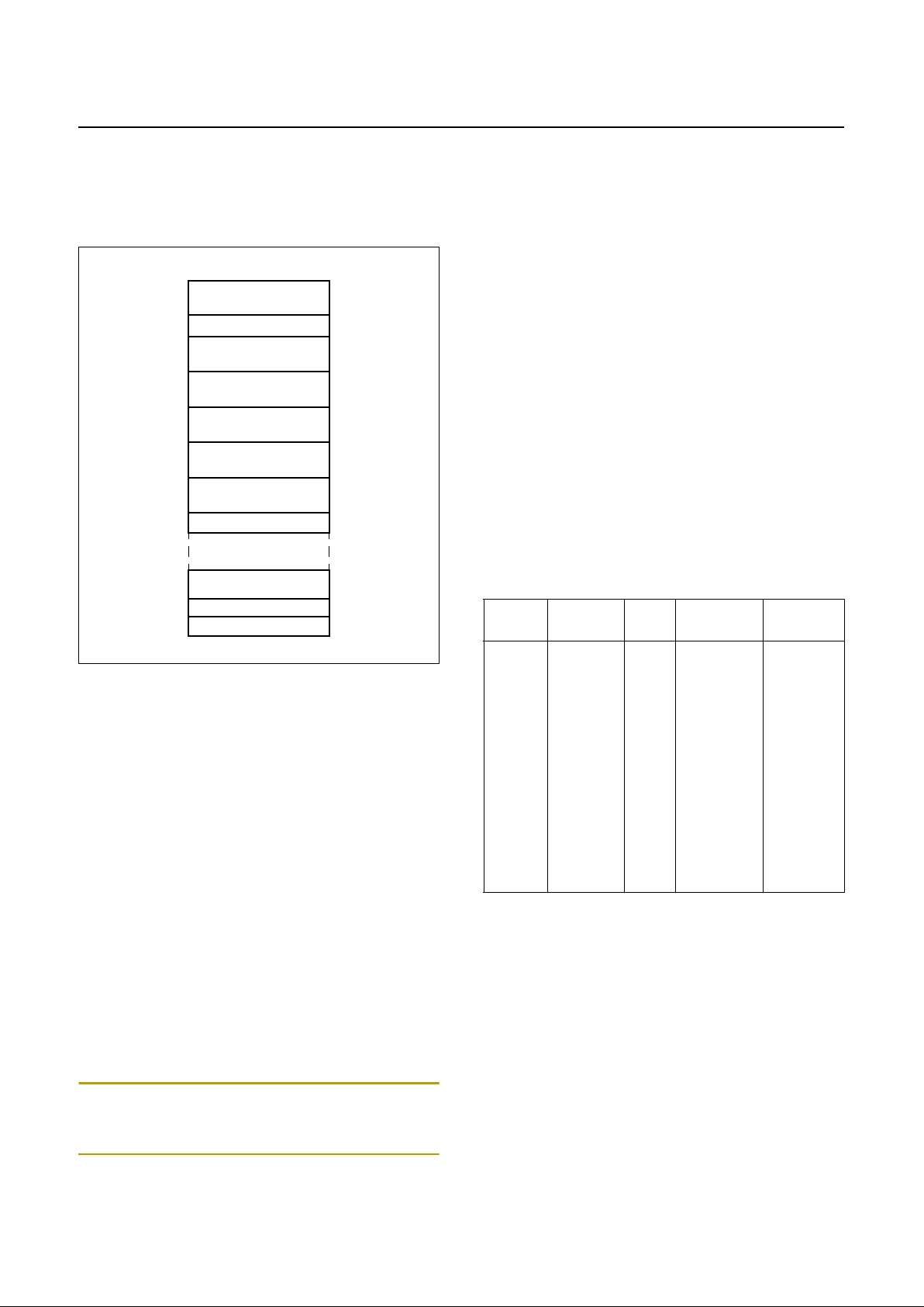
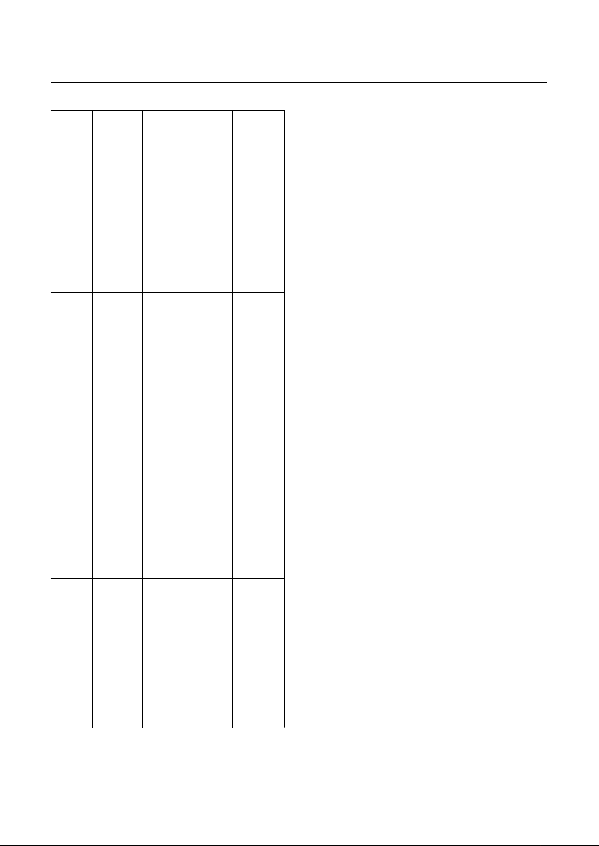
Figur e 8- 8 sho w s th e i nt er n a l D at a M emory sp ac e av ailable. Data Memory is di vided into four groups, a user RAM,
control registers, Stack, and OSD memory.
Figure 8-8 Data Memory Map
User Memory
The GMS81C4040/GM S87C4060 has 1,536 × 8 bits for
the user memory (RA M ).
Control Registers
The control registers are used by the CPU and Peripheral
function blocks for controlling the desired operat ion of the
device. Theref ore these regis ters contai n contr ol a nd sta tus
bits for the interru p t system, th e timer/ coun ters, analog to
digital conv ert ers and I /O po rts. The ba sic co ntro l regis t ers
are in address range of 00C0
H
to 00FFH. And OSD control
registers are assigned within 0AE0
H
~ 0AFFH.
Note that unoccupied addresses may not be implemented
on the chip . Re ad ac ce sse s to t hese add ress es w ill in g eneral return random data, and write accesses will have an indeterminate effect.
More detailed informations of each register are explained
in each peripheral section.
Note:
Write only registers can not be accessed by bit manipulation inst ruct ion . Do not use read- modi fy-wr ite i nstruc tion. Use byte manipulation instruction.
Example; To write at CKCTLR
LDM CLCTLR,#09H ;Divide ratio ÷8
Stack Area
The stack pro vides the area where the return address is
saved before a jump is performed du ring the pro cessing
routine at the execution of a subroutine call instruction or
the acceptance of an in terrupt.
When returning from the processing routine, executing the
subroutine re turn inst ruction [RET ] restores t he contents of
the program counter fro m the stack; executing the int errupt
return instruction [RETI] restores the contents of the program counter and flags.
The save/restore locations in the stack are determined by
the stack pointed (SP). The SP is automatically decreased
after the saving, and increased before the restoring. This
means the value of the SP indicates the stack location
number for the next save. Refer to Figure 8-4 on page 19.
Page0
RAM (192 bytes)
Peripheral Reg. (64 bytes)
0100H
00C0H
0000H
RAM (256 bytes)
0200H
RAM (256 bytes)
0300H
RAM (256 bytes)
0400H
RAM (256 bytes)
0500H
RAM (256 bytes)
0600H
RAM (64 bytes)
0A00H
OSD RAM (192 bytes)
0AE0H
Peripheral Reg. (32 bytes)
0C00H
Sprite RAM (96 bytes)
Empty area
Page1
Page2
Page3
Page4
Page5
Page6
PageA
PageC
063FH
Stack area
0C5FH
Address Symbol R/W Reset Value
Addressing
mode
00C0H
00C1H
00C2H
00C3H
00C4H
00C5H
00C8H
00C9H
00CAH
00CBH
00CCH
00CDH
00CEH
00CFH
R0
R0DD
R1
R1DD
R2
R2DD
R4
R4DD
R5
R5DD
R6
R6DD
FUNC1
FUNC2
R/W
W
R/W
W
R/W
W
R/W
W
R/W
W
R/W
W
W
W
????????
00000000
????????
00000000
????????
00000000
????????
0000---????????
----0000
?------0-------
-0000000
---00000
byte, bit
1
byte
2
byte, b it
byte
byte, b it
byte
byte, b it
byte
byte, b it
byte
byte, b it
byte
byte
byte
Table 8-1Control reg isters
Page 28
GMS81C4040/87C4060
PRELIMINARY
24
PRELIMINARY
Nov. 1999 Ver 1.0
0D0H
0D1H
0D2H
0D3H
0D4H
0D5H
0D6H
0D7H
0D8H
0D9H
0DAH
0DBH
0DCH
0DEH
0DFH
TM0
TM2
TDR0
TDR1
TDR2
TDR3
BITR
CKCTLR
WDTR
ICAR
ICDR
ICSR
ICCR1
ICCR2
SIOM
SIOR
R/W
R/W
R/W
R/W
R/W
R/W
R
W
W
R/W
R/W
R/W
R/W
R/W
R/W
R/W
-0000000
-0000000
????????
????????
????????
????????
????????
--010111
-0111111
00000000
11111111
000100000000000
00000000
-0000001
????????
byte
byte
byte, bi t
byte, bi t
byte, bi t
byte, bi t
byte
byte
byte
byte, bi t
byte, bi t
byte, bi t
byte, bi t
byte, bi t
byte, bi t
byte, bi t
0E0H
0E1H
0E2H
0E3H
0E4H
0E5H
0E8H
0E9H
0EAH
0EBH
0EEH
0EFH
PWMR0
PWMR1
PWMR2
PWMR3
PWMR4
PWMR5
PWM8H
PWM8L
PWMCR1
PWMCR2
BUR
AIPS
W
W
W
W
W
W
R/W
R/W
R/W
R/W
W
W
????????
????????
????????
????????
????????
????????
????????
--??????
00000000
--0-0000
????????
--000000
byte
byte
byte
byte
byte
byte
byte, bi t
byte, bi t
byte, bi t
byte, bi t
byte
byte
0F0H
0F1H
0F2H
0F3H
0F4H
0F5H
0F6H
0F7H
0F9H
0FAH
0FBH
0FCH
0FDH
ADCM
ADR
IEDS
IMOD
IENL
IRQL
IENH
IRQH
IDCR
IDFS
IDR
DPGR
TMR
R/W
R
W
R/W
R/W
R/W
R/W
R/W
R/W
R
R
R/W
W
--011101
????????
--000000
--000000
0000000000000000000000
00000000
0000-000
1----001
????????
----0000
????????
byte, bi t
byte
byte
byte, bi t
byte, bi t
byte, bi t
byte, bi t
byte, bi t
byte, bi t
byte
byte
byte, bi t
byte
0AE0H
0AE1H
0AE2H
0AE3H
0AE4H
0AE5H
0AE6H
0AE8H
0AE9H
0AF0H
0AF1H
0AF3H
0AF4H
OSDcon1
OSDcon2
OSDPOL
FDWSET
EDGEcol
OSDLN
LHPOS
SPVPOS
SPHPOS
L1ATTR
L1VPOS
L2ATTR
L2VPOS
R/W
R/W
W
W
W
R
W
W
W
W
W
W
W
00000000
-0000000
????????
01111010
10000111
---00000
????????
????????
????????
????????
????????
????????
????????
byte, bi t
byte, bi t
byte
byte
byte
byte
byte
byte
byte
byte
byte
byte
byte
Table 8-1Control registers
1. "byte, bit" means that register can be addressed by not only bit
but byt e manipulation instruction.
2. "byte" means that register can be addressed by only byte
manipulation instruction. On the other hand, do not use any
read-modify-write instruction such as bit manipulation for clearing bit .
Page 29

PRELIMINARY
GMS81C4040/87C4060
Nov. 1999 Ver 1.0
PRELIMINARY
25
8.4 Addressing Mode
The GMS800 series uses six addressing modes;
• Register addressing
• Immediate addressing
• Direct page addressing
• Absolute addressing
• Indexed addressing
• Register-indirect addressing
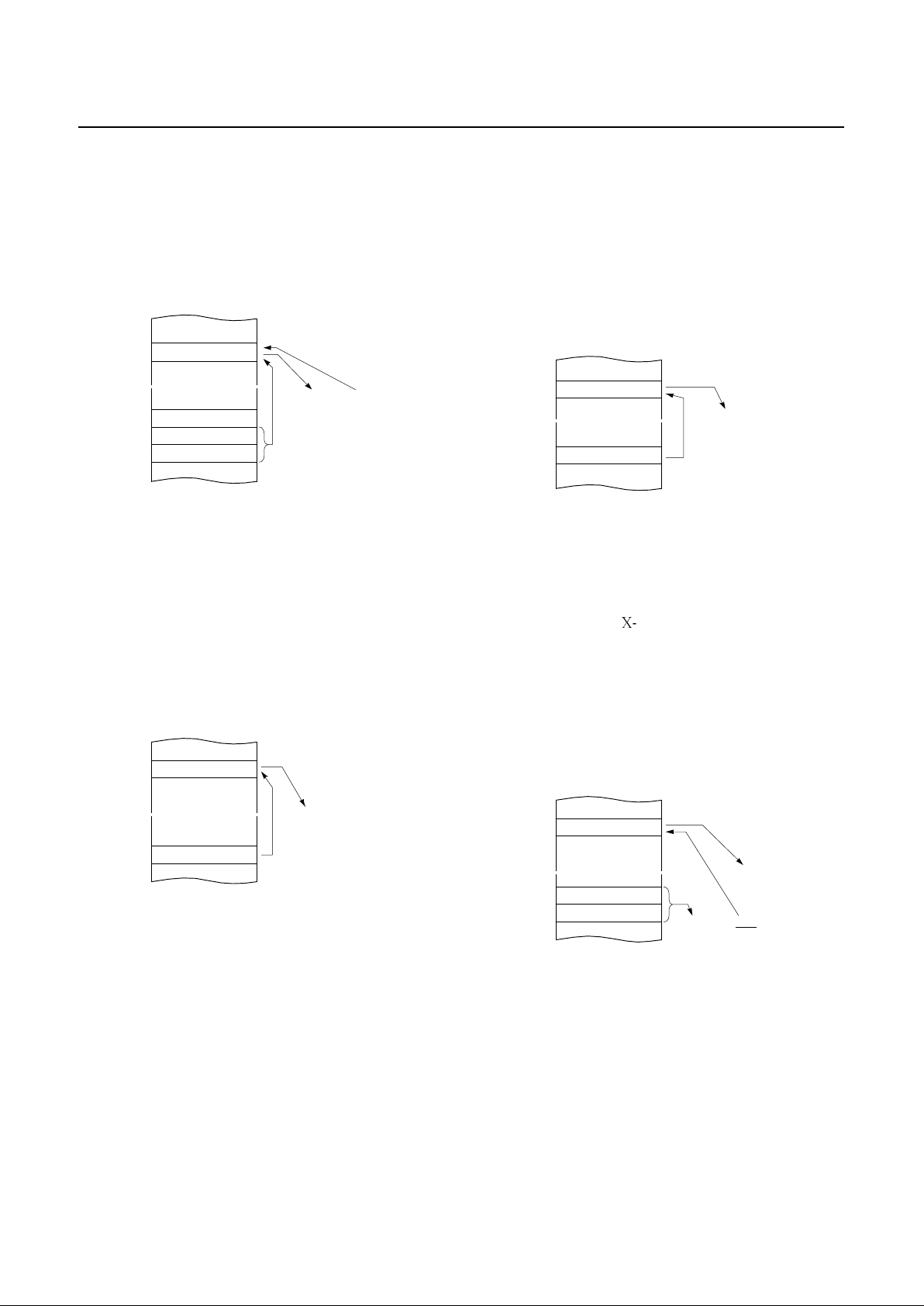
(1) Register Addressing
Register addressin g accesses the A, X, Y, C and PSW.
(2) Immediate Addressing →
→ →
→ #imm
In this mode, second byte (operand) is accessed as a data
immed iatel y.
Exam ple:
FE10: 0435 ADC #35H
When G-flag is 1, then RAM address is defined by 16-bit
address which is composed of 8-bit direct page accessable
register (DPGR) and 8-bit immediate data.
Example: G=1, DPGR=0CH
F100: E45535 LDM 35H,# 55H
(3) Direct Page Addressing →
→ →
→ dp
In this mode, a address is specified within direc t page.
Example; G=0
E551: C5 35 LDA 35H;A ←RAM[35H]
(4) Absolute Addressing →
→ →
→ !abs
Absolute addr essing sets corr esponding memor y data to
Data , i.e. second byte(Operand I) of command becomes
lower level address and third byte (Operand II) becomes
upper level address.
With 3 bytes command, it is possible to access to whole
memory area.
ADC, AND, CMP, CMPX, CMPY, EOR, LDA, LDX,
LDY, OR, SBC, STA, STX, STY
Example;
F100: 07 35 F0 ADC!0F 035H ;A ←ROM[0F035H]
35
A+35H+C → A
04
MEMORY
0FE10
H
E4
0F100
H
data
←
55H
~
~
~
~
data
0C35
H
þ
35
0F102
H
550F101
H
A
data
35
35
H
0E551
H
data → A
À
þ
~
~
~
~
C5
0E550
H
07
0F100
H
~
~
~
~
data0F035
H
P
F0
0F102
H
350F101
H
A
A+data+C → A
address: 0F035
Page 30
GMS81C4040/87C4060
PRELIMINARY
26
PRELIMINARY
Nov. 1999 Ver 1.0
The operation within data memory (RAM)
ASL, BIT, DEC, INC, LSR, ROL, ROR
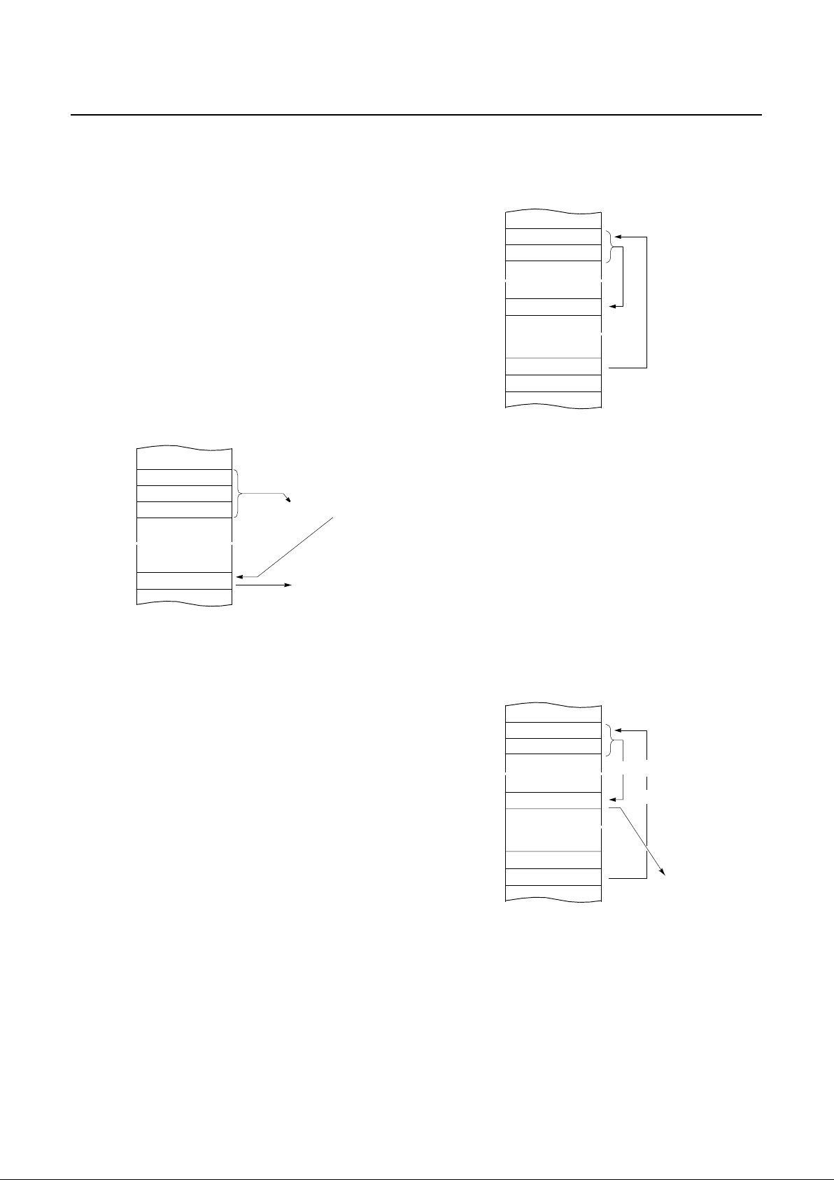
Exam ple; A dd res sing ac cesses t he a ddre ss 0 135
H
regard-
less of G-flag and DPGR.
F100: 983501 INC!0135H ;A ←ROM[135H]
(5) Indexed Addressing
X indexe d di rec t pa g e (no of f set ) →
→ →
→ {X}
In this mode, a address is specified by the X register.
ADC, AND, CMP, EOR, LDA, OR, SBC, STA, XMA
Example; X=15
H
, G=1, DPGR=03
H
E550: D4 LDA {X};ACC←RAM[X].
X indexed direct page, auto increment→
→ →
→ {X}+
In this mode, a address is specified within direct page by
the X register and the content of X is increased by 1.
LDA, STA
Example; G=0, X=35
H
F100: DB LDA {X}+
X indexed direct page (8 bit offset) →
→ →
→ dp+X
This address value is the second byte (Operand) of command plus the data of -register. And it assigns the memory in Direct page.
ADC, AND, CMP, EOR , LDA, LDY, OR, SBC, STA
STY, XMA, ASL, D EC, INC, LSR, ROL, RO R
Example; G=0, X=0F5
H
E550: C6 45 LDA 45H+X
98
0F100
H
~
~
~
~
data135
H
þ
01
0F102
H
350F101
H
À
data+1 → data
Ã
address: 0135
data
D4
315
H
0E550
H
data → A
À
þ
~
~
~
~
data
DB
35
H
data → A
À
þ
~
~
~
~
36H → X
0F100
H
data
45
3A
H
0E551
H
data → A
À
þ
~
~
~
~
C6
0E550
H
45H+0F5H=13AH
Ã
Page 31
PRELIMINARY
GMS81C4040/87C4060
Nov. 1999 Ver 1.0
PRELIMINARY
27
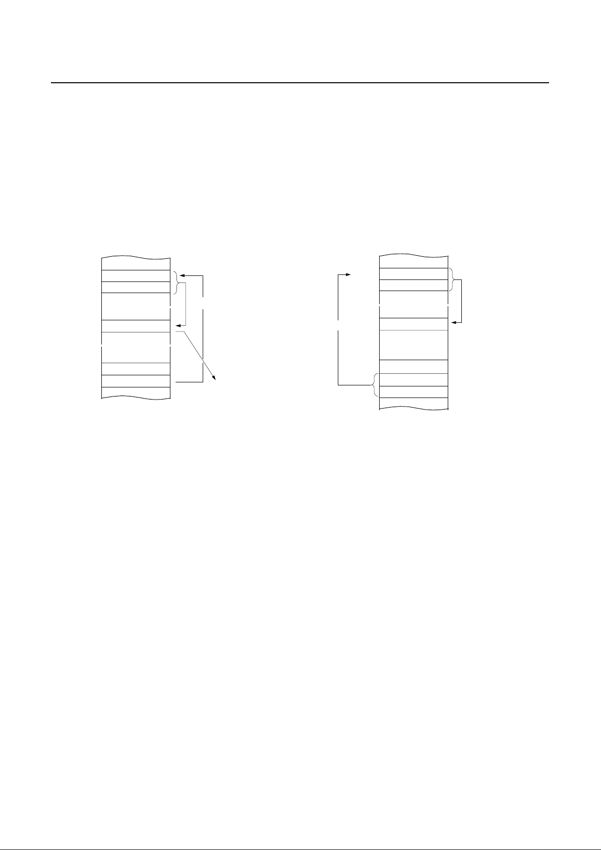
Y indexe d di rec t pa g e (8 bit off se t) →
→ →
→ dp+Y
This address value is the second byte (Operand) of command plus the data of Y-register , which assign s Memory in
Direct page.
This is same with above (2). Use Y register instead of X.
Y indexed absolute →
→ →
→ !abs+Y
Sets the value of 16 -bit absolute address plus Y-register
data as Memory. This addressing mode can specify memory in whole area.
Example; Y=55
H
F100: D500FA LDA !0FA0 0H+Y
(6) Indirect Addressing
Direct pa ge in di rec t →
→ →
→ [dp]
Assigns data address to use for accomplishing command
which sets memory data(or pair memory) by Operand.
Also index can be used with Index register X,Y.
JMP, CALL
Example; G=0
FA00: 3F 35 JMP [35H]
X indexed indirect →
→ →
→ [dp+X]
Processes memory data as Data, assigned by 16-bit pair
memory which is determined by pair data
[dp+X+1][dp+X] Operand plus X-register data in Direct
page.
ADC, AND, CMP, EOR, LDA, OR, SBC, STA
Example; G=0, X=10
H
FA00: 16 25 ADC [25H+X]
D5
0F100
H
data → A
þ
~
~
~
~
data
0FA55
H
0FA00H+55H=0FA55H
Ã
FA
0F102
H
00
0F101
H
À
0A
35
H
jump to address 0E30A
H
þ
~
~
~
~
35
0FA00
H
E3
36
H
À
3F
0E30A
H
NEXT
~
~
~
~
05
35
H
0E005
H
~
~
~
~
25
0FA00
H
E0
36
H
16
0E005
H
data
~
~
~
~
Ã
A + data + C → A
25 + X(10) = 35
H
þ
À
Page 32
GMS81C4040/87C4060
PRELIMINARY
28
PRELIMINARY
Nov. 1999 Ver 1.0
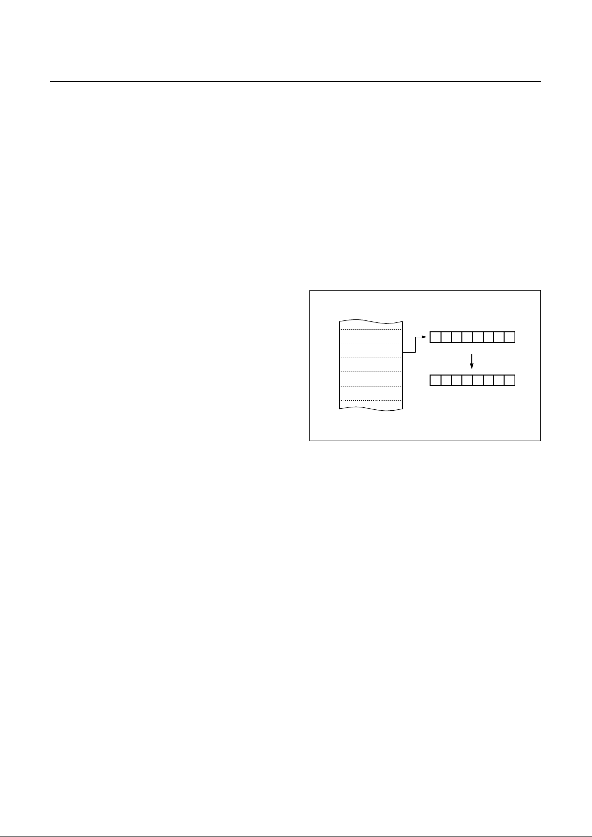
Y indexed indirect →
→ →
→ [dp]+Y
Processes momory data as Data, assigned by the data
[dp+1][dp] of 16-bit pair memory paired by Operand in Direct page plus Y-register data.
ADC, AND, CMP, EOR, LDA, OR, SBC, STA
Example; G=0, Y=10
H
FA00: 1725 ADC [25H]+Y
Absolute indirect →
→ →
→ [!abs]
The program jumps to a ddres s speci fied by 16-b it a bsolu te
address .
JMP
Example; G=0
FA00: 1F 25 E0 JMP [!0C025 H]
05
25
H
0E005H + Y(10) = 0E015
H
þ
~
~
~
~
25
0FA00
H
E026
H
À
17
0E015
H
data
~
~
~
~
Ã
A + data + C → A
25
0E025
H
jump to
~
~
~
~
E0
0FA00
H
E70E026
H
À
25
0E725
H
NEXT
~
~
~
~
1F
PROGRAM MEMORY
þ
address 0E30A
H
Page 33
PRELIMINARY
GMS81C4040/87C4060
Nov. 1999 Ver 1.0
PRELIMINARY
29
9. I/O PORTS
The GMS 81C4040/G MS87C406 0 has dig ital ports (R0,
R1, R2, R4, R5 and R6) and OSD ports (R,G,B) .
These ports pins may be mul tiplexed with an alte rnate
function for the peripheral features on the device. In general, in a initial reset state, R ports are used as a general
purpose digital port.
9.1 Registers for Port
Port Data Registers
The Port Data Registers in I/O buffer in each R ports are
represented as a Type D fli p-flop, whic h will clo ck in a va lue from the internal bus in re spons e to a "write to data register" signa l from the CPU. T he Q outpu t of the fl ip-f lop is
placed on the internal bus in response to a "read data register" signal from the CPU. The level of the port pin itself
is placed on the internal bus in response to "read data register" signal from the CPU. Some instructions that read a
port activating the "read register" signal, and others activating the "read pin" signal
Port Direction Registers
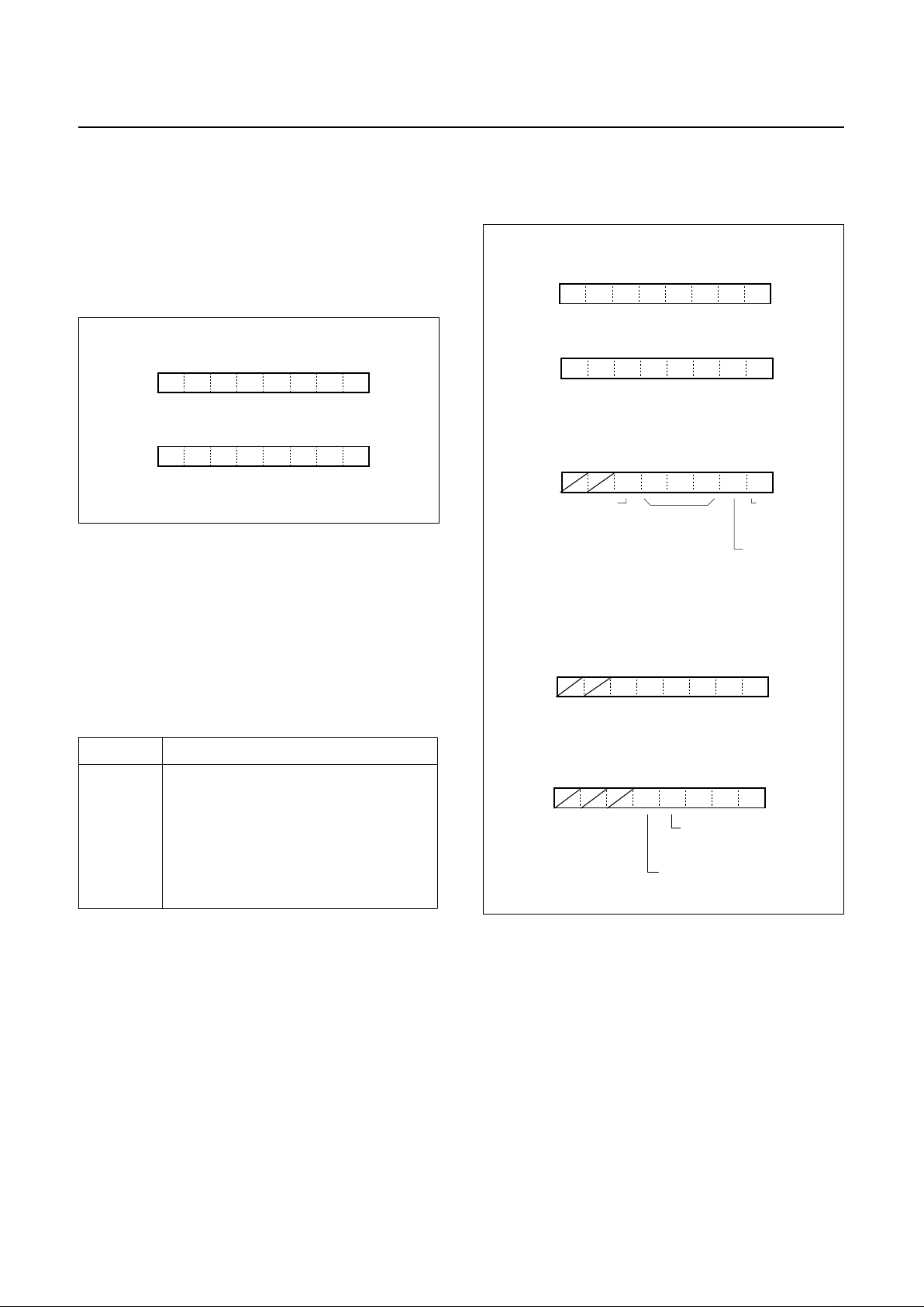
All pi ns have data directio n registe rs which c an define
these ports as output or input. A "1" in the port direction
register c onfigure the corr esponding por t pin as output.
Conversely, write "0" to the corresponding bit to speci f y it
as input pin. For example, to use the even numbered bit of
R0 as output ports and the odd numbered bits as input
ports, write "55
H
" to address 0C1H (R0 port direction reg-
ister) during ini tial setting as shown in Figure 9-1 .
All the port directio n registers in the GMS81C404 0/
GMS87C4060 have 0 wr itten to t hem by reset function. On
the other hand, its init ial status is in put.
Figure 9-1 Example of port I/O assignment
I : INPUT PORT
WRITE "55
H
" TO PORT R0 DIRECTION REGISTER
0 1 0 1 0 1 0 1
I O I O I O I O
R0 DATA
R4 DATA
R0 DIRECTION
R4 DIRECTION
0C0H
0C1H
0C8H
0C9H
76543210
BIT
76543210
PORT
O : OUTPUT PORT
~
~
~
~
Page 34
GMS81C4040/87C4060
PRELIMINARY
30
PRELIMINARY
Nov. 1999 Ver 1.0
9.2 I/O Ports Configuration
R0 Ports
R0 is an 8-bit CM OS bidirectional I/O po rt (address
0C0
H
). Each I/O pin can independe ntl y used as an input or
an output through the R0DD regis ter (address 0C1
H
).
The control registers for R0 are shown below.
In addition, Port R0 is only digital I/O. After reset, R0DD
value is "0", R0 acts as normal digital input port.
R1 Ports
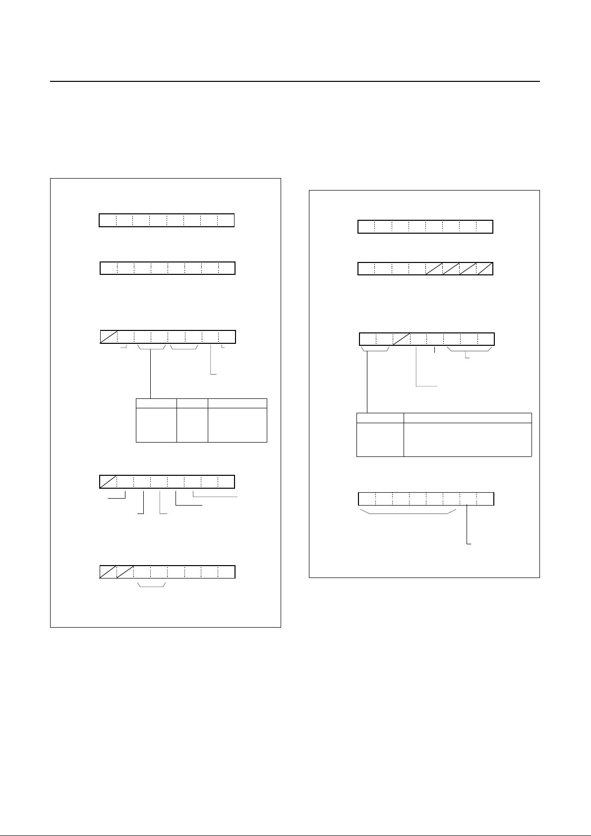
R1 is an 8-bit CM OS bidirectional I/O po rt (address
0C2
H
). Each I/O pin can independe ntl y used as an input or
an output through the R1DD regis ter (address 0C3
H
).
R1 port have secondary functions as following table.
The cont rol registers for R1 are shown b elow.
Port R1 is multiplexed with various special features.The
control registers contro ls the selection of alternate function. After reset, R1 port acts as normal digital input port.
The way to select alternate function such as A/D input or
HD,VD will be shown in each peripheral section.
Port Pin Alternate Function
R10
R11
R12
R13
R14
R15
R16
R17
AN0 (A/D input 0)
AN1 (A/D input 1)
AN2 (A/D input 2)
AN3 (A/D input 3)
AN4 (A/D input 4)
AN5 (A/D input 5)
VD (Vertical Sync. input)
HD (Horizontal Sync. input)
R0 Data Register
R0
ADDRESS : 00C0
H
RESET VALUE : Undefined
R07 R06 R05 R04 R03 R02 R01 R00
Port Direction
R0 Direction Register
R0DD
ADDRESS : 00C1
H
RESET VALUE : 0000 0000
b
0: Input
1: Output
RW RW RW RW RW RW RW RW
WWWWWWWW
R1 Data Register
R1
ADDRESS : 00C2
H
RESET VALUE : Undefined
R17
R16 R15 R14 R13
R12 R11 R10
Port Direction
R1 Direction Register
R1DD
ADDRESS : 00C3
H
RESET VALUE : 0000 0000
b
0: Input
1: Output
A/D Convertor mode Register
ADCM
ADDRESS : 00F0
H
RESET VALUE : --01 1101
b
Port Property
Analog input pin selector Register
AIPS
ADDRESS : 00EF
H
RESET VALUE : --00 0000
b
0: Digital I/O
1: Analog Input
R16/VD select
Port function select Register 2
FUNC2
ADDRESS : 00CF
H
RESET VALUE : ---0 0000
b
0: R16 I/O
1: VD Input
ADEN ADS2 ADS1 ADS0 ADST ADSF
HDS
VDS YMS YSS IS
A/D Status
0: Busy
1: Finish
A/D Start
0: Ignore
1: A/D sta rt
A/D Port select
000: AN0
001: AN1
A/D Enable
0: Disable
1: Enable
010: AN2
011: AN3
100: AN4
101: AN5
110: AN6
111: No Analog port
R17/HD select
0: R17 I/O
1: HD Input
RW RW RW
RW
RW RW RW RW
RW RW
RW RW RW R
WWWWWWWW
WWWWWW
WWWWW
Page 35
PRELIMINARY
GMS81C4040/87C4060
Nov. 1999 Ver 1.0
PRELIMINARY
31
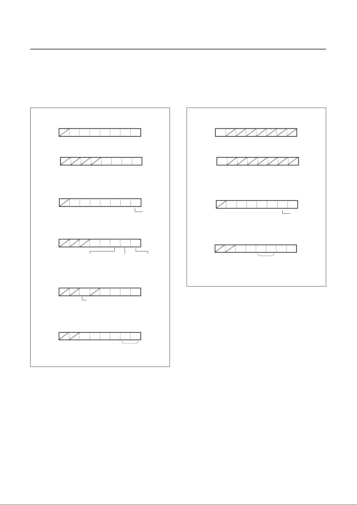
R2 Port
R2 is an 8-bit CM OS bidirectional I/O po rt (address
0C4
H
). Each I/O pin can independe ntl y used as an input or
an output through the R2DD regi ster (address 00C5
H
).
The control registers for R2 are shown below.
R4 Port
R4 is consrutced with 4-bi t Open dra in Output port and 4bit CMOS bidirectional I/O port (address 0C8
H
). Each I/O
pin can independently used as an input or an output
through the R4DD register (address 0C9
H
).
The cont rol registers for R4 are shown b elow.
R2 Data Register
R2
ADDRESS : 00C4
H
RESET VALUE : Undefined
R27
R26 R25 R24 R23
R22 R21 R20
Port Direction
R2 Direction Register
R2DD
ADDRESS : 00C5
H
RESET VALUE : 0000 0000
b
0: Input
1: Output
Serial I/O mode Register
SIOM
ADDRESS : 00DE
H
RESET VALUE : -000 0001
b
00: Ignore edge
Ext. interrupt edge selection Register
IEDS
ADDRESS : 00F2
H
RESET VALUE : --00 0000
b
01: Falling edge
10: Rising edge
R20/INT2
Port function select Register 1
FUNC1
ADDRESS : 00CE
H
RESET VALUE : -000 0000
b
0: R20
1: INT2
SM1 SM0 SCK1 SCK0 SIOST SIOSF
INT4S
INT3S INT2S INT1S INT0S
Seriial Status
0: Busy
1: Finish
Serial Start
0: Ignore
1: Serial start
Clock select
00: PS3
01: PS4
Serial I/O
0: Serial In
1: Serial Out
10: PS5
11: External
IOSW
EC2SEC3S
SM1
0
0
1
1
SM0
0
1
0
1
Mode
Send
Receive
-
R21
R21
Sclk
Sclk
R21
R22
R22
Sout
R22
R22
R23
R23
R23
Sin
R23
R24/INT3
0: R24
1: INT3
R26/INT4
0: R26
1: INT4
R27/EC3
0: R27
1: EC3
R25/EC2
0: R25
1: EC2
IED2H IED2L IED1H IED1L IED0H IED0L
11: Falling/Rising edge
INT2
RW RW RW
RW
RW RW RW RW
WWWWWWWW
RW RW RW RW RW RW R
WWWWWWW
WWWWWW
R4 Data Register
R4
ADDRESS : 00C8
H
RESET VALUE : Undefined
R47 R46 R45 R44 R4 3 R42 R41 R40
Port Direction
R4 Direction Register
R4DD
ADDRESS : 00C9
H
RESET VALUE : 0000 ----
b
0: Input
1: Output
I2C Control Register 1
ICCR1
ADDRESS : 00DB
H
RESET VALUE : 00-0 0000
b
EN5,4,3,2,1 : R47,45,43,42,41,40
PWM control Register 1
PWMCR1
ADDRESS : 00EA
H
RESET VALUE : 0000 0000
b
0: R4x acts normal digital port
1: R4x acts PWM output port
ALS ESO BC2 BC1 BC0
EN2
EN1 EN0 EN8 CNT
Bit count
000
b
(8bit)
I2C enable
0: Disable
1: Enable
BSW0
EN3EN4EN5
BSW1
0
0
1
1
BSW0
0
1
0
1
R44
R44
SCL0
R44
SCL
R45
R45/PWM4
R45/PWM4
SCL1
SCL
R46
R46
SDA0
R46
SDA
BSW1
001b~111b (1~7bit)
R47
R47/PWM5
R47/PWM5
SDA1
SDA
Slave address identification
0: Accept (Addressing format)
1: Decline (Free data format)
RW RW RW RW RW RW RW RW
WWWWWWWW
RW RW RW RW RW RW RW
RW RW RW RW RW RW RW RW
14/8bit PWM count
0: Count start
1: Count stop
R51/PWM8 select
0: R51
1: PWM8
Page 36
GMS81C4040/87C4060
PRELIMINARY
32
PRELIMINARY
Nov. 1999 Ver 1.0
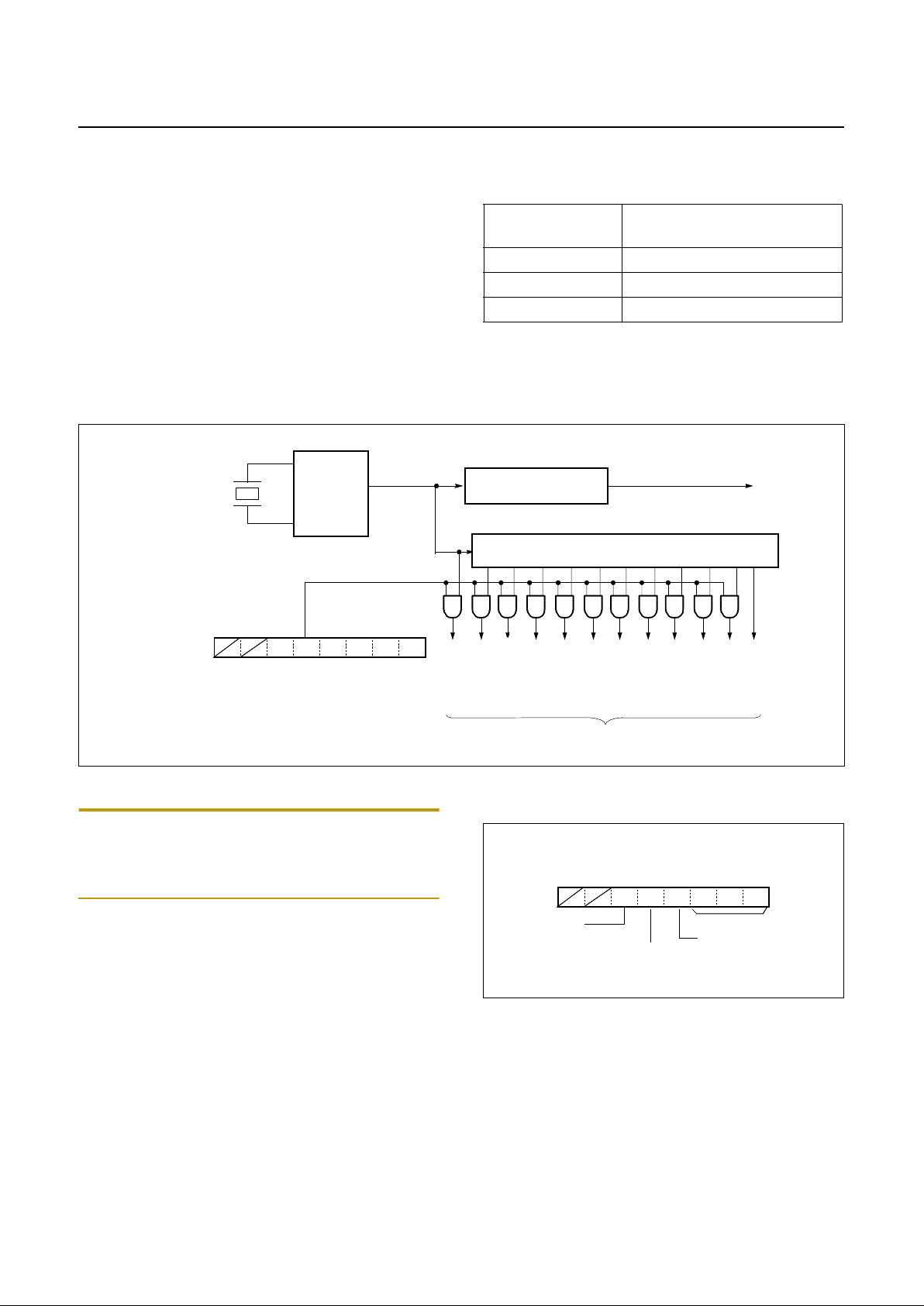
R5 Port
R5 is an 7-bit port (addre ss 0CA
H
). Each I/O pin can independently used a s an input or an output through the R5DD
register (address 0CB
H
).
The control regist ers for R5 are shown below
R6 Port
R6 is an 1-bit CMOS bidirectional I/O port (address
0CC
H
). Each I/O pin c an indepe ndentl y use d as an input or
an output through the R6DD register (address 0CD
H
).
The cont rol registers for R6 are shown b elow
R5 Data Register
R5
ADDRESS : 00CA
H
RESET VALUE : Undefined
R56 R55 R54 R53
R52 R51
R50
Port Direction
R5 Direction Register
R5DD
ADDRESS : 00CB
H
RESET VALUE : ---- 0000
b
0: Input
1: Output
00: Ignore edge
Ext. interrupt edge selection Register
IEDS
ADDRESS : 00F2
H
RESET VALUE : --00 0000
b
01: Falling edge
10: Rising edge
R52/INT0
Port function select Register 1
FUNC1
ADDRESS : 00CE
H
RESET VALUE : -000 0000
b
0: R52
1: INT0
INT4S INT3S INT2S INT1S INT0SEC2SEC3S
IED2HIED2L IED1H IED1L IED0H IED0L
11: Falling/Rising edge
R56/I
Port function select Register 2
FUNC2
ADDRESS : 00CF
H
RESET VALUE : ---0 0000
b
0: R56
1: I Output
HDS
VDS YMS YSS IS
R55/YS
0: R55
1: YS Output
R54/YM
0: R56
1: YM Output
PWM control Register 2
PWMCR2
ADDRESS : 00EB
H
RESET VALUE : --0- 0000
b
POL2 POL1 EN7 EN6BUZS
INT2
R50/BUZZ
0: R50
1: BUZZ
RW RW RW
RW RW RW RW
WWWW
WWWWWWW
WWWWW
RW RW RW RW RW
WWWWWW
R6 Data Register
R6
ADDRESS : 00CC
H
RESET VALUE : Undefined
Port Direction
R6 Direction Register
R6DD
ADDRESS : 00CD
H
RESET VALUE : 0--- ----
b
0: Input
1: Output
00: Ignore edge
Ext. interrupt edge selection Register
IEDS
ADDRESS : 00F2
H
RESET VALUE : --00 0000
b
01: Falling edge
10: Rising edge
R67/INT1
Port function select Register 1
FUNC1
ADDRESS : 00CE
H
RESET VALUE : -000 0000
b
0: R67
1: INT1
INT4S IN T3S INT2S INT1S IN T0SEC2SEC3S
IED2HIED2L IED1H IED1L IED0H IED0L
11: Falling/Rising edge
INT1
RW
WWW
WWWW
WWWWWW
R67
W
Page 37
PRELIMINARY
GMS81C4040/87C4060
Nov. 1999 Ver 1.0
PRELIMINARY
33
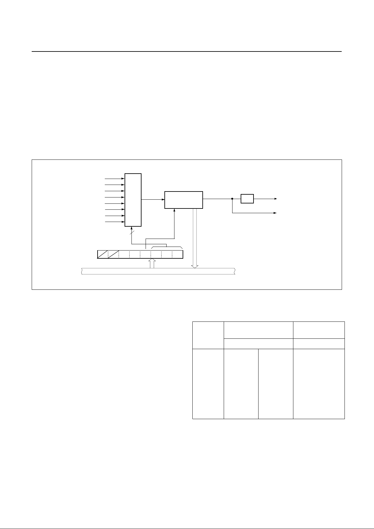
10. CLOCK GENERATOR
As shown in Fi gure 10- 1 , t he cl ock gen erator prod uces the
basic clock pulses which provide the system clock to be
supplied to the CPU and the peripheral hardware. It contains two oscil lators: a main-f requency cl ock oscilla tor and
a sub-freq uency clock oscillator. The syste m clock can
also be obtained from the external oscillator.
The clock generator produces the system clocks forming
clock pulse, whi ch ar e supp lied to the CPU and t he peri pheral hardware.
To the peripheral block, the clock among the not-divided
original clocks, divided by
2
, 4,...,
up to 1024 can be provided. Peripheral clock is enabled or disabled by bit 4 of
the peripheral clo ck en able register (ENPCK).
Figure 10-1 Block Diagram of Clock Generator
Note:
On the initial reset, all peripherals are run because
peripheral clock is supplied to each function block. If you
want to see more detai ls, see Clock Control Register
(CKCTLR).
Main clock
Minimum instruction cycle time
(ex:NOP ; f
ex
4clock is needed)
3.6MHz 1,111nS
4MHz 1,000nS
8MHz 500nS
Internal system clock
PRESCALER
ENPCK
÷
1
Peripheral clock
f
EX
Clock control register
[0D6
H
]
CKCTLR
WDT
ENPCKBTCL BTS2 BTS1 BTS0
Clock pu lse Gener a tor
ON
OSC
Circuit
PS0
PS1
PS2
PS3
PS4
PS5
PS6
PS7
PS8
PS9
PS10
PS11
÷2 ÷4 ÷8 ÷16 ÷32 ÷64 ÷
128 ÷256 ÷512 ÷1024 ÷2048
Clock control register
ADDRESS : 00D6
H
RESET VALUE : --01 0111
b
CKCTLR
WDT
ENPCKBTCL BTS2 BTS1 BTS0
ON
Peri. Clock
0: Stop
1: Supply
Watch-dog
timer select
0: Normal 6bit timer
1: Watch-dog timer
B.I.T set
0: Free run
1: B.I.T clear
B.I.T Clock
WWWWWW
Page 38
GMS81C4040/87C4060
PRELIMINARY
34
PRELIMINARY
Nov. 1999 Ver 1.0
11. TIMER
11.1 Basic Interval Timer
The GMS81C4040/GMS87C4060 has one 8-bit Basic Interval Timer that is free-run and can not be stopped. Block
diagram is shown in Figure 11-1 .
The Basic Interval Timer generates the time base for
watchdog timer counting, and etc. It also provides a Basic
inte rval timer interr upt (BIT IF). As t he count overflo w
from FF
H
to 00H, this overflow causes the interrupt to be
generated. The Basic Interval Timer is controlled by the
clock control register (CKCTLR) shown in Figure 11-2 .
Source clock can be sele cted by lower 3 bits of CKCTLR.
BITR and CKCTLR are located at same address, and ad-
dress 00D6
H
is read as a BITR and written to CKCTLR..
Figure 11-1 Block Diagram of Basi c Interval Timer
Table 11-1 Basic Interval Timer Interrupt Time
MUX
Basic Interval Timer Interrupt
BITR
Select Input clock
3
source
clock
8-bit up-counter
BITCK
BTCL
f
ex
÷
2
10
f
ex
÷
2
9
f
ex
÷
2
8
f
ex
÷
2
7
f
ex
÷
2
6
f
ex
÷
2
5
f
ex
÷
2
4
Watchdog timer clock (WDTCK)
clear
overflow
Internal bus line
[0D6H]
[0D6
H
]
BITIF
Clock control register
CKCTLR
WDT
ENPCKBTCL BTS2 BTS1 BTS0
ON
PS4
PS5
PS6
PS7
PS8
PS9
PS10
PS11
f
ex
÷
2
11
BTS2~0
Source clock
Interrupt
(overflow) Perio d
Pre-Scaler output
At fex=8MHz
000
001
010
011
100
101
110
111
PS4
PS5
PS6
PS7
PS8
PS9
PS10
PS11
f
ex
÷
2
4
f
ex
÷
2
5
f
ex
÷
2
6
f
ex
÷
2
7
f
ex
÷
2
8
f
ex
÷
2
9
f
ex
÷
2
10
f
ex
÷
2
11
0.512
1.024
2.048
4.096
8.192
16.384
32.768
65.536
mS
Page 39
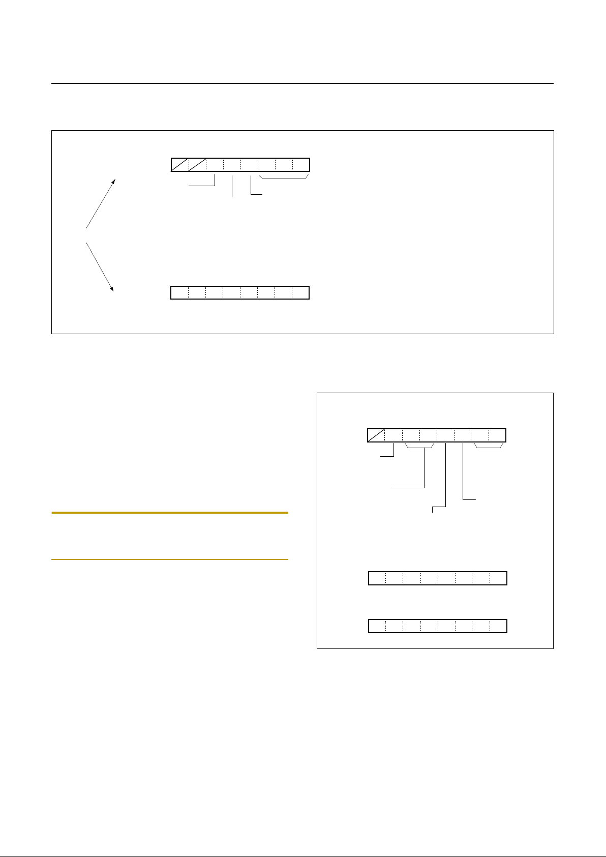
PRELIMINARY
GMS81C4040/87C4060
Nov. 1999 Ver 1.0
PRELIMINARY
35
Figure 11-2 BITR: Basic Int erval Timer Mode Register
11.2 Tim er 0, 1
Timer 0, 1 c onsist s of pres caler , multip lexer, 8-bit c ompar e
data register, 8-bit count register, Control register, and
Comparator as shown in Figure 11-3 .
These Timers can run separated 8bit timer or comb ined
16bit timer. These timers are operated by internal clock.
The co ntents of TDR1 are com pare d with th e cont ents of
up-counter T1. If a match is found, a timer/ counte r 1 interrupt (T1IF) is ge nerate d, and the co unter is c leared. Coun ting up is resumed after the counter is cleared.
Note:
You can read Timer 0, Timer 1 value from TDR0 or
TDR1. But if you write data to TDR0 or TDR1, it changes
Timer 0 or Timer 1 modulo data, not Ti m er val ue.
The c ont ent of TDR 0, T DR 1 m ust be i nit iali ze d (b y soft ware) with the value between 01
H
and FFH,not to 00H.
Or not, Timer 0 or Timer 1 can not count up forever.
The control registers for Timer 0,1 are shown below.
CKCTLR
INITIAL VALUE: Undefined
ADDRESS: 00D6
H
BITR
Both register are in same address,
when write, to be a CKCTLR,
when read, to be a BITR.
Caution
:
8-BIT BINARY COUNTER
ADDRESS : 00D6
H
RESET VALUE : --01 0111
b
WDT
ENPCK BTCL BTS2 BTS1 BTS0
ON
Peri. Clock
0: Stop
1: Supply
Watch-dog
timer select
0: Normal 6bit timer
1: Watch-dog timer
B.I.T set
0: Free run
1: Clear 8-bit counter (BITR) to "0". This bit becomes 0
B.I.T Clock
automatically after 1 machine cycle
WWWWWW
RRRRRRRR
Timer mode register 0
TM0
ADDRESS : 00D0
H
RESET VALUE : -000 0000
b
Timer 0 data register
TDR0
ADDRESS : 00D2
H
RESET VALUE : Undefined
T1SL0 T0ST T0CN T0SL1 T0SL0T1SL1T1ST
Timer 1 data register
TDR1
ADDRESS : 00D3
H
RESET VALUE : Undefined
Timer 0 input clock
00: PS2 (f
ex
/ 22)
01: PS4 (f
ex
/ 24)
10: PS6 (f
ex
/ 26)
11: PS8 (f
ex
/ 28)
Timer 1 input clock
00: Timer 0 overflow (16bit mode)
01: PS2 (f
ex
/ 22)
10: PS4 (f
ex
/ 24)
11: PS6 (f
ex
/ 26)
0: Count Hold
1: Count Continue
Timer 0 control
0: Count Hold
1: Count Clear and Start
Timer 0 start
0: Count Hold
1: Count Clear and Start
Timer 1 start
RW RW RW RW
RW RW RW
RW RW RW RW RW RW RW RW
RW RW RW RW RW RW RW RW
Page 40
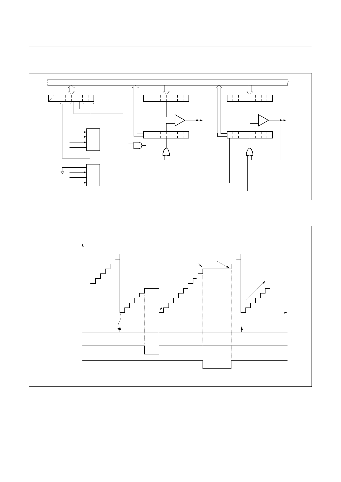
GMS81C4040/87C4060
PRELIMINARY
36
PRELIMINARY
Nov. 1999 Ver 1.0
.
Figure 11-3 Simplified Block Diagram of 8bit Timer0, 1
Figure 11-4 Count Example of Timer
8bit Comparator
Internal bus line
TM0 TDR0
Timer 0
T0IF
Clock
TDR1
Timer 1
ClockClear Clear
8bit Comparator
T1IF
MUX
PS2
PS4
PS6
PS8
MUX
NC
PS2
PS4
PS6
T0CN
T0ST
T1ST
Timer 0 (T0IF)
Interrupt
TDR0
TIME
Occur interrupt Occur interrupt
stop
clear & start
disable
enable
Start & Stop
T0ST
T0CN
Contr ol co unt
u
p-c
o
u
nt
~
~
~
~
T0ST = 0
T0ST = 1
T0CN = 0
T0CN = 1
Page 41
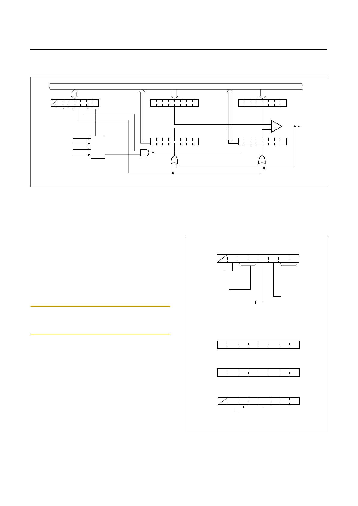
PRELIMINARY
GMS81C4040/87C4060
Nov. 1999 Ver 1.0
PRELIMINARY
37
Figure 11-5 Simplifi ed Block Diagram of 16bit Timer0, 1
11.3 Timer / Event Counter 2, 3
Timer 2, 3 c onsist s of pres caler , multip lexer, 8-bit c ompar e
data register, 8-bit count register, Control register, and
Comparator as shown in Figure 11-5 .
These Timers have two operating modes. One is the timer
mode which is operated by internal c lock, other is event
counter mode whic h is operat ed by extern al cl ock from pin
R25/EC2, R27/EC3.
These Timers can run separated 8bit timer or comb ined
16bit timer.
Note:
You can read Timer 2, Timer 3 value from TDR2 or
TDR3. But if you write data to TDR2 or TDR3, it changes
Timer 2 or Timer 3 modulo data, not Ti m er val ue.
The c ont ent of TDR 2, T DR 3 m ust be i nit iali ze d (b y soft ware) with the value between 01
H
and FFH,not to 00H.
Or not, Timer 2 or Timer 3 can not count up forever.
The control registers for Timer 2,3 are shown below
Internal bus line
TM0 TDR0
Timer 0
Clock
TDR1
Timer 1
ClockClear Clear
16bit Comparator
T1IF
MUX
PS2
PS4
PS6
PS8
T0CN
T0ST
00
Timer mode register 2
TM2
ADDRESS : 00D1
H
RESET VALUE : -000 0000
b
Timer 2 data register
TDR2
ADDRESS : 00D4
H
RESET VALUE : Undefined
T3SL0
T2ST T2CN T2SL1 T2SL0T3SL1T3ST
Timer 3 data register
TDR3
ADDRESS : 00D5
H
RESET VALUE : Undefined
Timer 2 input clock
00: PS2 (f
ex
/ 22)
01: PS4 (f
ex
/ 24)
10: PS6 (f
ex
/ 26)
11: PS8 (f
ex
/ 28)
Timer 3 input clock
00: Timer 2 overflow (16bit mode)
01: PS2 (f
ex
/ 22)
10: PS4 (f
ex
/ 24)
11: PS6 (f
ex
/ 26)
0: Count Hold
1: Count Continue
Timer 2 control
0: Count Hold
1: Count Clear and Start
Timer 2 start
0: Count Hold
1: Count Clear and Start
Timer 3 start
Port function select Register 1
FUNC1
ADDRESS : 00CE
H
RESET VALUE : -000 0000
b
INT4S INT3S INT2S INT1S INT0SEC2SEC3S
R27/EC3
0: R27
1: EC3
R25/EC2
0: R25
1: EC2
RW RW RW RW RW RW RW
RW RW RW RW RW RW RW RW
RW RW RW RW RW
RW RW
RW
WWWW
WWW
Page 42
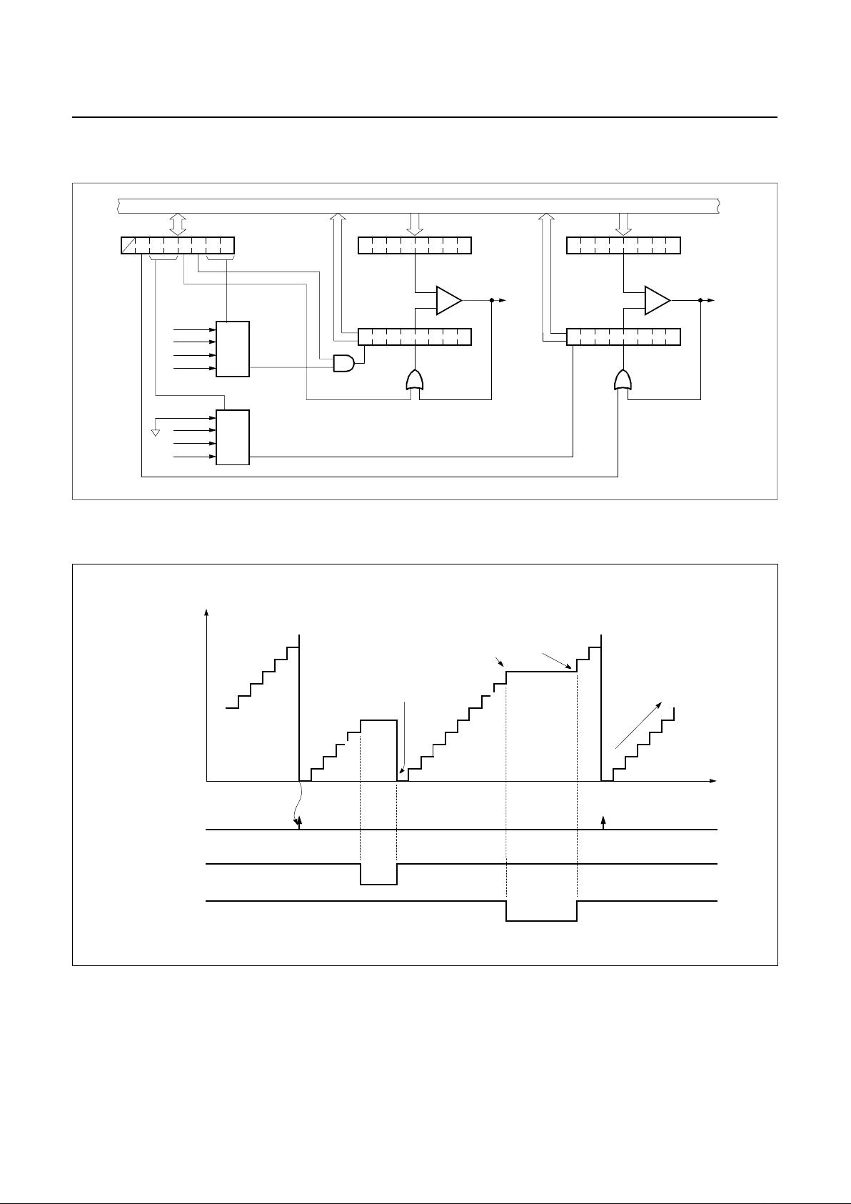
GMS81C4040/87C4060
PRELIMINARY
38
PRELIMINARY
Nov. 1999 Ver 1.0
.
Figure 11-6 Simplified Block Diagram of 8bit Timer/Event Counter 2,3
Figure 11-7 Count Example of Ti me r / Event counter
8bit Comparator
Internal bus line
TM2 TDR2
Timer 2
T2IF
Clock
TDR3
Timer 3
ClockClear Clear
8bit Comparator
T3IF
MUX
EC2
PS2
PS4
PS6
MUX
NC
EC3
PS2
PS4
T2CN
T2ST
T3ST
Timer 2 (T2IF)
Interrupt
TDR2
TIME
Occur interrupt Occur interrupt
stop
clear & start
disable
enable
Start & Stop
T2ST
T2CN
Contr ol co unt
u
p-c
o
u
nt
~
~
~
~
T2ST = 0
T2ST = 1
T2CN = 0
T2CN = 1
Page 43
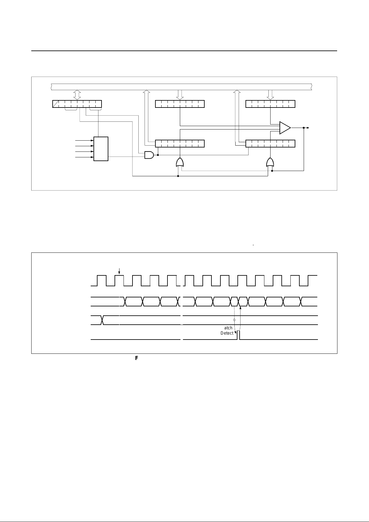
PRELIMINARY
GMS81C4040/87C4060
Nov. 1999 Ver 1.0
PRELIMINARY
39
Figure 11-8 Simplified Block Diagram of 16bit Timer/Event Counter 2,3
Timer Mode
In the timer mode, the internal clock is used for counting
up. Thus, you can think of it as counting internal clock input. The c ontents of TDRn (n=0~3) are compared with the
contents of up-counter, Timer n. If match is found, a timer
n interrupt (T nIF) is generated and the up -counter is
cleared to 0. Counting up is resumed after the up-counter
is clea r ed.
As the value of TDRn is changeable by software, time interval is set as you want
Figure 11-9 Timer Mode Timing Chart
Event counter Mode
In event timer mode, counting up is started by an external
trigger. This tr igger mea ns falling edg e of the ECn (n =2~3)
pin input. Source cl ock is used as an inte rnal clock selected
with TM2. The contents of TDRn are compared with the
contents of the up-count er. If a match is fou nd, an TnIF interrupt is generated, and the counter is cleared to 00
H
. The
counter is restarted by the falling edge of the ECn pin in-
put.
The maximum frequency applied to the E Cn pin is f
ex
/2
[Hz] in main clock mode.
In order to use event counter function, the bit EC2S, EC3
of the Port Function Select Register1 FUNC1(address
0CE
H
) is required to be set to "1".
After reset, the value of TDRn is undefined, it should be
Internal bus line
TM2 TDR2
Timer 2
Clock
TDR3
Timer 3
ClockClear Clear
16bit Comparator
T3IF
MUX
EC2
PS4
PS6
PS8
T0CN
T0ST
00
0
N-2
2
0
N
3
N-1
N
~
~
~
~
~
~
Source clock
Up-counter
TDRn (n=0~3)
TnIF (n=0~3) interrupt
Start co un t
~
~
123
~
~
~
~
1 4
Match
Detect
Counter
Clear
Page 44
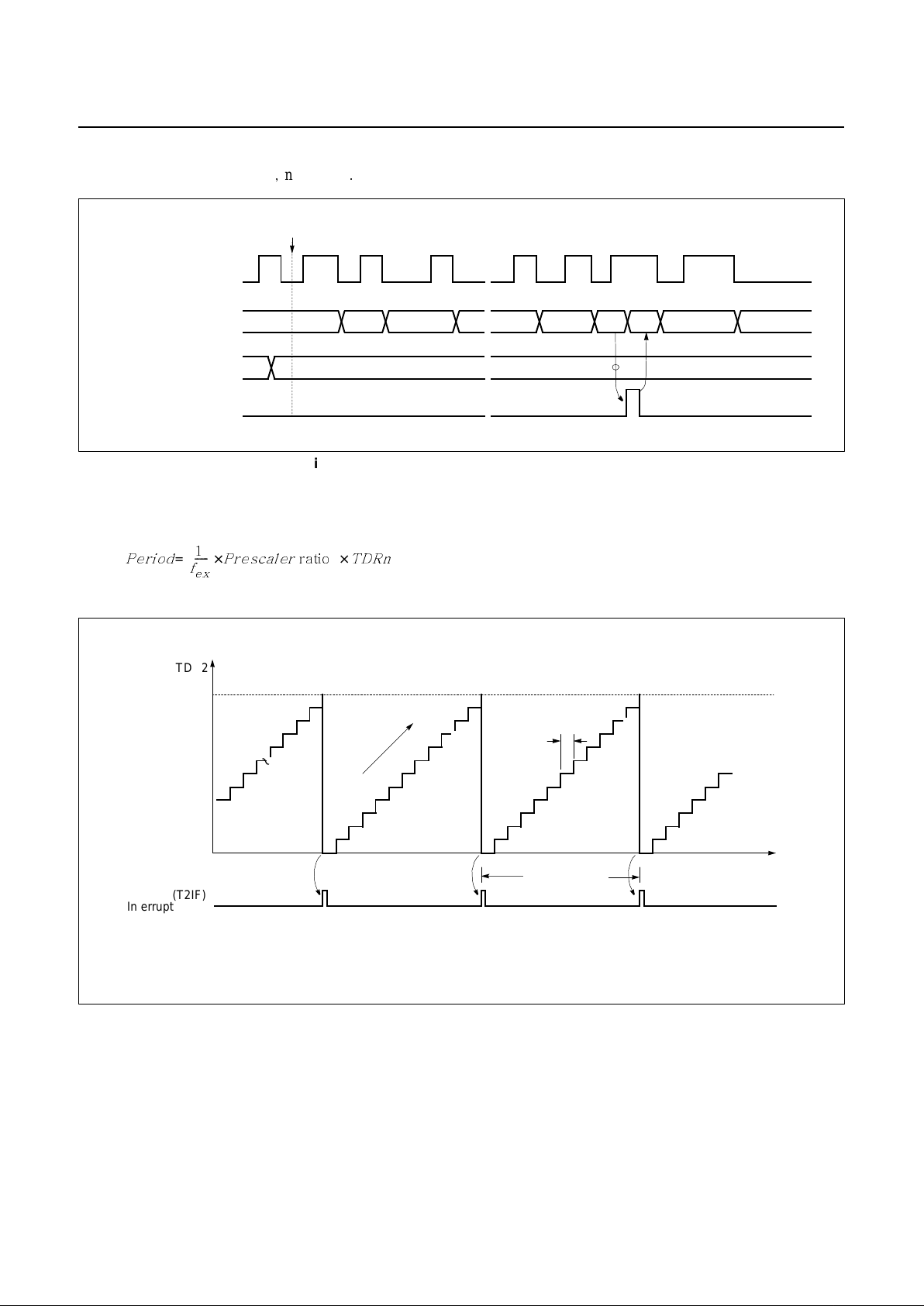
GMS81C4040/87C4060
PRELIMINARY
40
PRELIMINARY
Nov. 1999 Ver 1.0
initialized to between 01H~FFH
not to 00H
Figure 11-10 Event Counter M ode Timing Chart
The interval period of Timer is calculated as below equation.
Figure 11-11 Count Exampl e of Timer / Event counter
0
1
2
1
0N
2
~
~
~
~
~
~
N-1
N
~
~
~
~
~
~
ECn (n=2~3) pin
Up-counter
TDRn ( n=2~3)
TnIF (n=2~3) interrupt
Start count
--------
×
×
=
~
~
Timer 2 (T2IF)
Interrupt
TDR2
TIME
Occur interrupt Occur interrupt Occur interrupt
Interrupt period
u
p
-coun
t
~
~
~
~
0
1
2
3
4
5
6
7
8
n
n-1
P
CP
= P
CP
x n
n-2
TDR2=n
Page 45
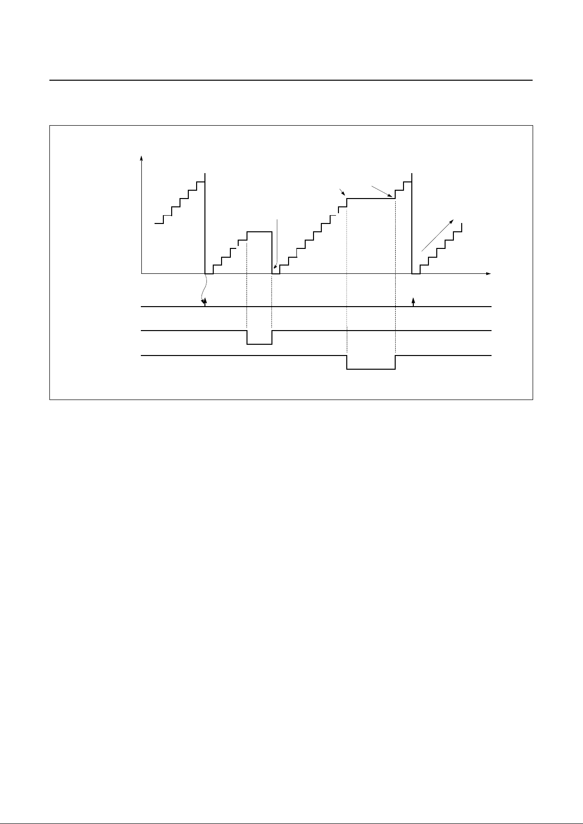
PRELIMINARY
GMS81C4040/87C4060
Nov. 1999 Ver 1.0
PRELIMINARY
41
Figure 11-12 Count Operat ion of Timer / Event counter
Timer 2 (T2IF)
Interrupt
TDR2
TIME
Occur interrupt Occur interrupt
stop
clear & start
disable
enable
Start & Stop
T2ST
T2CN
Contr ol co unt
up-coun
t
~
~
~
~
T2ST = 0
T2ST = 1
T2CN = 0
T2CN = 1
Page 46
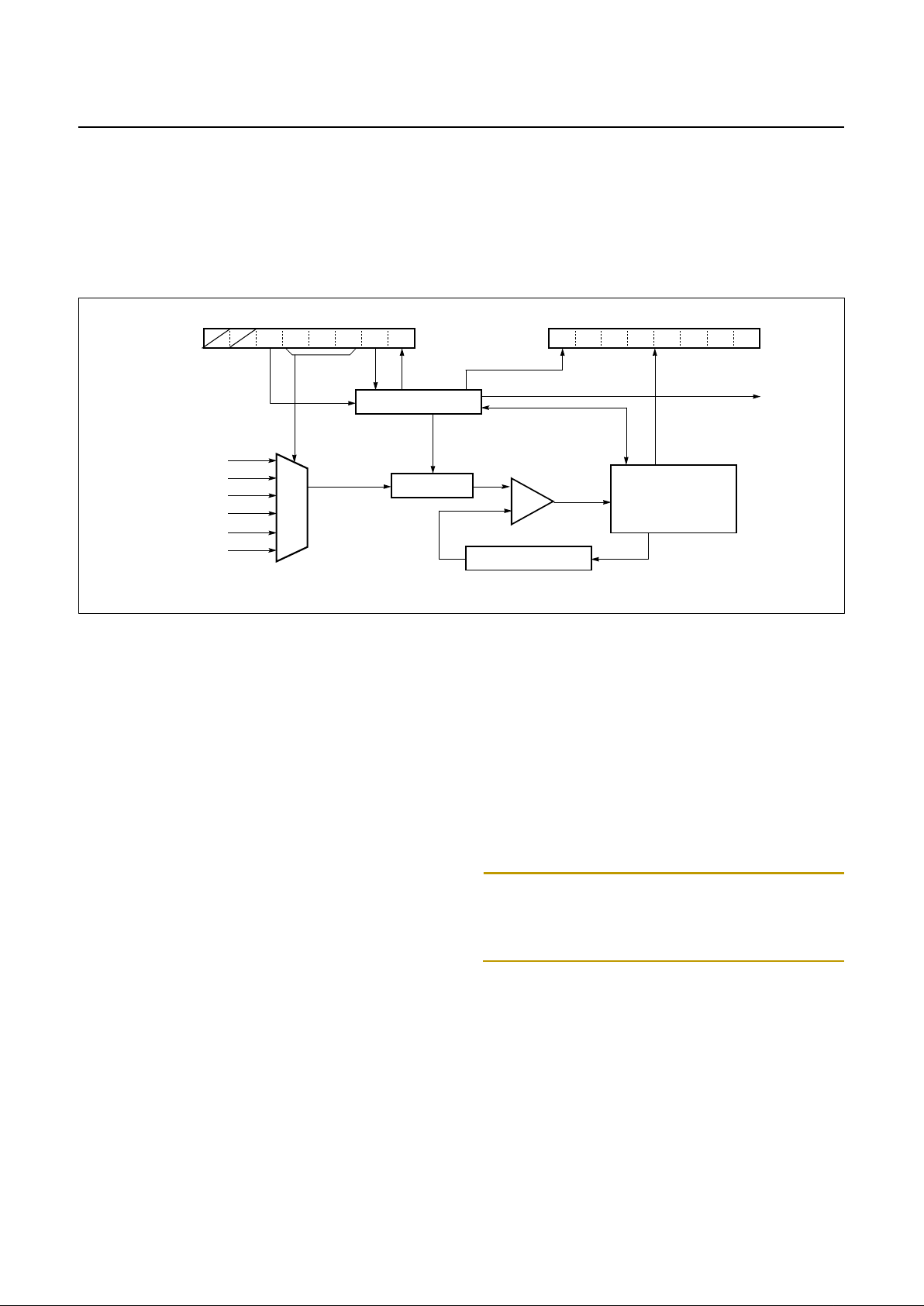
GMS81C4040/87C4060
PRELIMINARY
42
PRELIMINARY
Nov. 1999 Ver 1.0
12. A/D Converter
The A/D convertor circuit is shown in Figure 12-1 .
The A/D conve rtor ci rcuit c onsist s of the com par ator and
control register AIPS(00EF
H
), ADCM(00F0H),
ADR(00F1
H
). The AIPS register select normal port or an-
alog input. The ADCM register control A/D converter’s
activity. The ADR register stores A/D converted 8bit result. The more details are shown Figure 12-2 .
Figure 12-1 Block Diagram of A/D conv ertor circuit
Control
The GMS81C4040/GMS87C4060 contains a A/D converter module which has six analog inputs.
1. First of all , you hav e t o select an alog inp ut pi n by se t th e
ADCM and AIPS.
2. Set ADEN (A/D enable bit : ADCM bit5).
3. Set ADST (A/D start bit : ADCM bit1 ). We rec ommend
you do not set ADEN and ADST at once, it makes worse
A/D converted result.
4. ADST bit will be cleared automatic ally 1cy cle after you
set this.
Example:
:
; Set AIPS, cha ng e ? to what you wan t
; 0 : digital port
; 1 : analog port
LDM AIPS ,# 00 ?? ????b
; Set ADEN, xxx is analog port number
LDM ADCM ,# 00 1x xx00b
; or “SET1 ADEN”
; Set ADST, xxx is analog port number
LDM ADCM ,# 00 1x xx10b
; or “SET1 ADST”
:
:
5. After A/D conversi on is compl et ed, ADSF bit an d int errupt flag IFA will be set. (A/D conversion takes 36 machine cycle : 9uS when f
ex
=8MHz).
Note:
Make sure AIPS bits, if you using a port which is s et
digital input by AIPS, analog voltage will be flow into MCU
internal logic not A/D converter. Sometimes devi ce or port
is damaged permanently.
Comparator
AN0
MUX
AN1
AN2
AN3
port
select
+
−
S/H
ADCM [F0
H
]
ADEN ADS2 ADS1 ADS0 ADST ADSF
ADR [F1H]
AN4
AN5
Control circuit
Register ladder
Succesive
Approximation
Circuit
IFA
Vref
Page 47
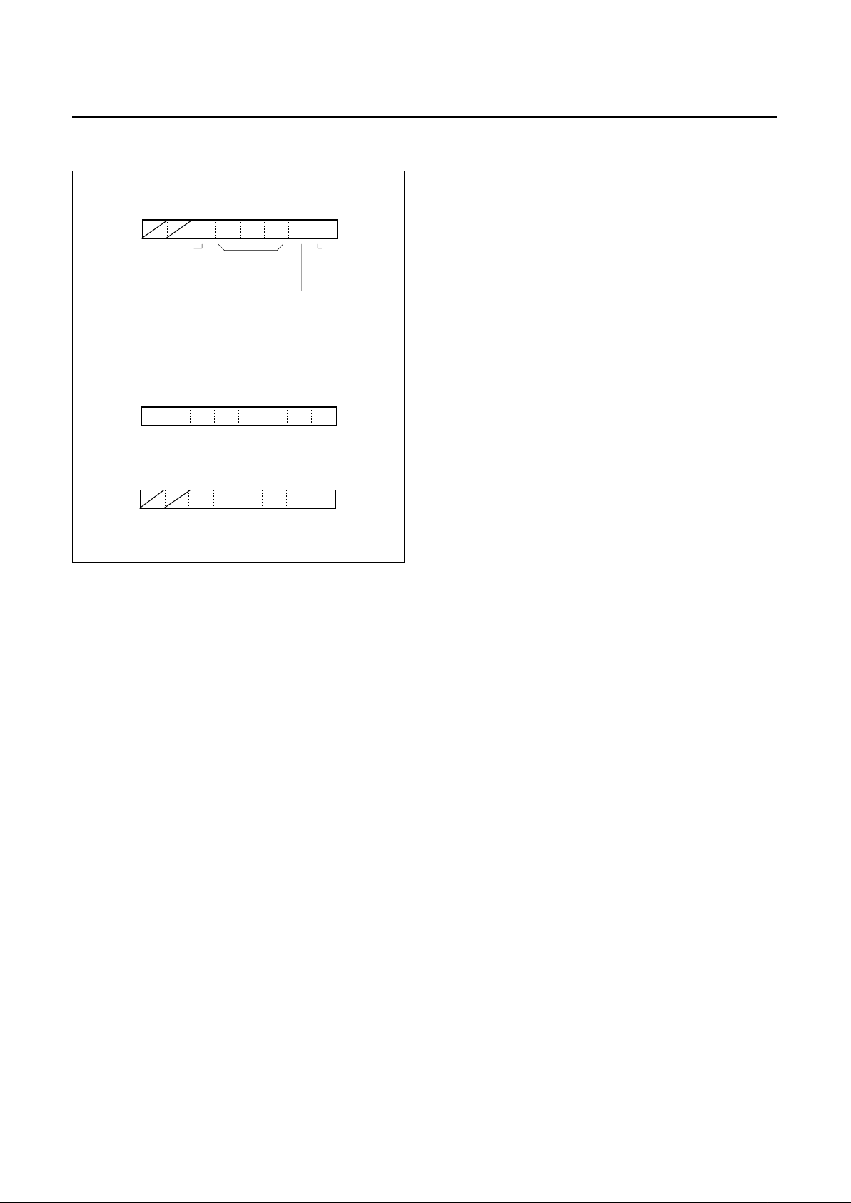
PRELIMINARY
GMS81C4040/87C4060
Nov. 1999 Ver 1.0
PRELIMINARY
43
Figure 12-2 A/D convertor Registers
A/D Result Register
ADR
ADDRESS : 00F1
H
RESET VALUE : Undefined
A/D Convertor mode Register
ADCM
ADDRESS : 00F0
H
RESET VALUE : --01 1101
b
Port Property
Analog input pin selector Register
AIPS
ADDRESS : 00EF
H
RESET VALUE : --00 0000
b
0: Digital I/O
1: Analog Input
ADEN ADS2 ADS1 ADS0 ADST ADSF
A/D Status
0: Busy
1: Finish
A/D Start
0: Ignore
1: A/D start
A/D Port select
000: AN0
001: AN1
A/D Enable
0: Disable
1: Enable
010: AN2
011: AN3
100: AN4
101: AN5
11x: No Analog port
8bit result is stored
RW RW RW
RW RW
R
RRRRRRRR
WWWWWW
Page 48
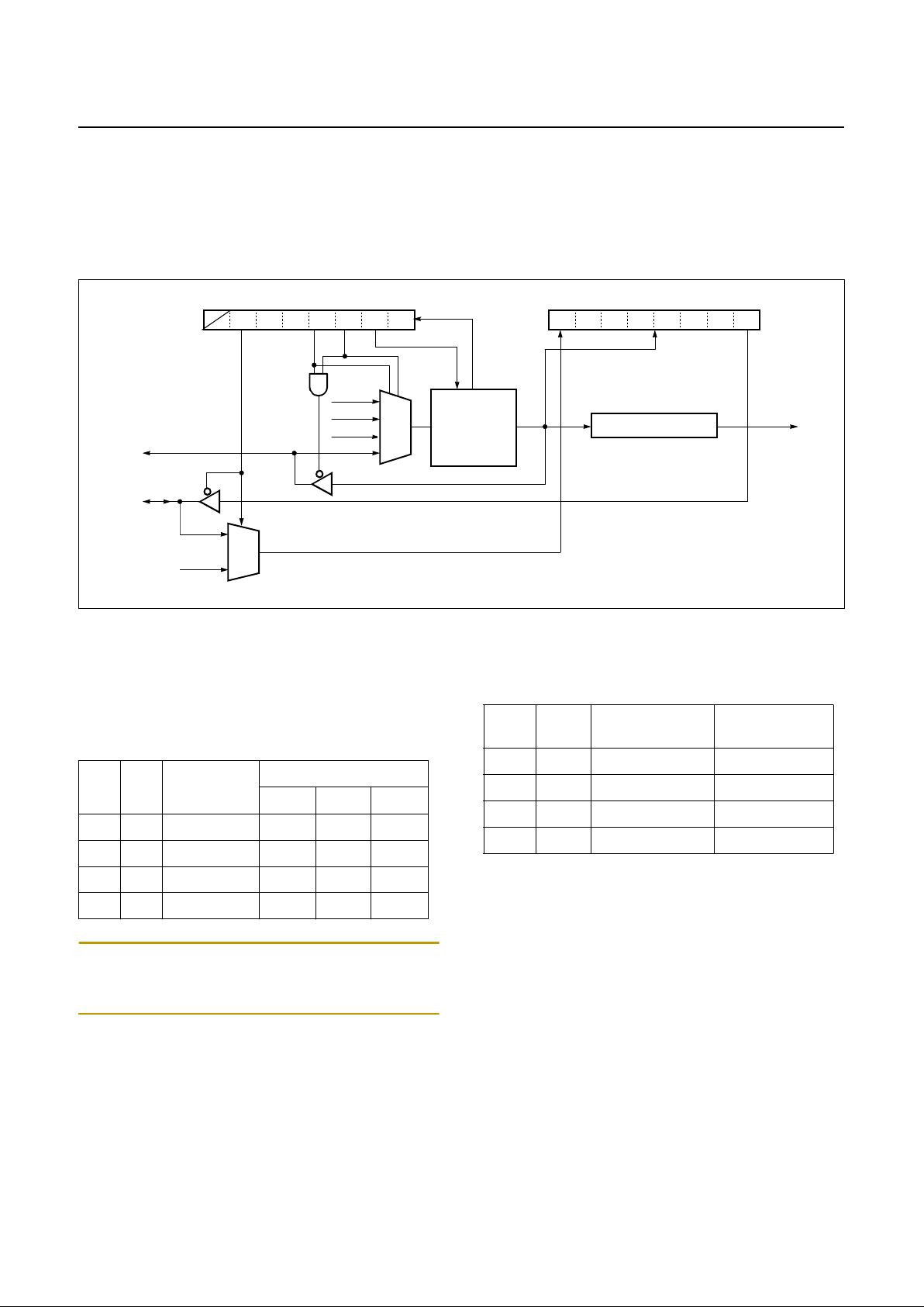
GMS81C4040/87C4060
PRELIMINARY
44
PRELIMINARY
Nov. 1999 Ver 1.0
13. Serial I/O
The Serial I/O circuit is shown in Figure 13-1 .
The Seria l I/O circu it consists o f the octal coun ter, SI-
OR(DF
H
), SIOM(DEH). The SIOR register stores received
data or data which will be transfered. The SIOM register
controls serial communication mode, speed, start, etc.
The more details about registers are shown Figur e 13-2 .
Figure 13-1 Block Diagram of Serial I/O circuit
Control
The GMS81C4040/GMS87 C4060 contains a Synchronous
type Serial I/O module.
1. You have to select serial I/O pins by set the SM1~0.
Note:
Sout pin can handle serial data output or serial data
input. You can input serial data to Sout pin when IOSW bit
is 1. But Sin pin is dedicated serial data input pin.
2. You have to sele ct serial c ommunicati on clock by s et the
SCK1~0.
3. If you want to send data, write it to SIOR. Or not skip
this.
4. Start serial communication by set SIOST(Serial I/O
start, SIOM bit1).
5
. After ser ial c ommunicati on is completed, SIOSF bit and
interrupt flag IFSIO will be set.
MUX
SIOM [DEH]
SM1 SM0 SCK1 SCK0 SIOST SIOSF
SIOR [DFH]
Sout
Sin
Octal counter
Control
Circuit
IFSIO
IOSW
1
0
MUX
PS3
PS5
PS4
Exclk
Sclk
D7 D6 D5 D4 D3 D2 D1 D0
SM1 SM0 Function
Port select
R21 R22 R23
00 - R21R22R23
0 1 Send Sclk Sout R23
10 Receive SclkR22Sin
11 - R21R22R23
SCK1 SCK0 Selected Clock
Ex: Frequency
(f
ex
=8MHz)
0 0 PS3 1uS
0 1 PS4 2uS
1 0 PS5 4uS
1 1 External clock User define
Page 49
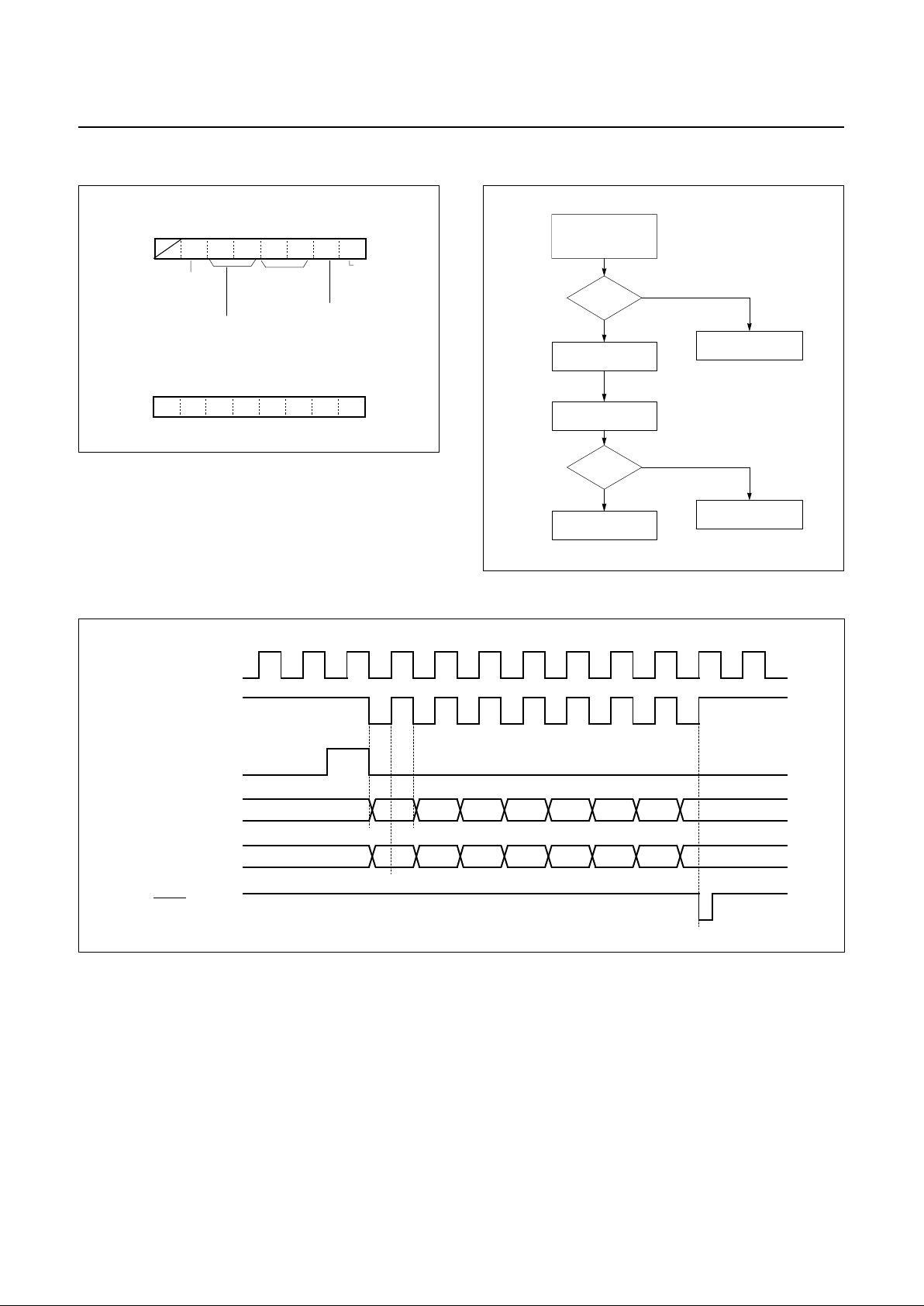
PRELIMINARY
GMS81C4040/87C4060
Nov. 1999 Ver 1.0
PRELIMINARY
45
Figure 13-2 Serial I/O Registers
Figure 13-3 Example for seri al I /O check by S/W
Figure 13-4 Serial I/O Timing Chart
Serial I/O data Register
SIOR
ADDRESS : 0DF
H
RESET VALUE : Undefined
Serial I/O mode Register
SIOM
ADDRESS : 0DE
H
RESET VALUE : -000 0001
b
Serial Status
0: Busy
1: Finish
Serial COMM. Start
0: Ignore
1: COMM. start
Input select
0: Sin
1: Sout
SM1 SM0 SCK1 SCK0 SIOST SIOSFIOSW
Clock Sel ect
Send / Receive
D7 D6 D5 D4 D3 D2 D1 D0
RW RW RW RW
RW RW
R
RW RW RW RW RW RW RW RW
Serial I/O Interrupt
Service routine
SIOSF=1?
SE=0
// SE : Interrupt enable bit
Abnormal operation
Write SIOM
SR=0?
// SR : Interrupt request flag
Normal operation
Overrun error
No
Yes
No
Yes
D0
Input clock
Sout
Sin
IFSIO
Sclk
SIOST
D1 D2 D3 D4 D5 D6 D7
D0 D1 D2 D3 D4 D5 D6 D7
Page 50
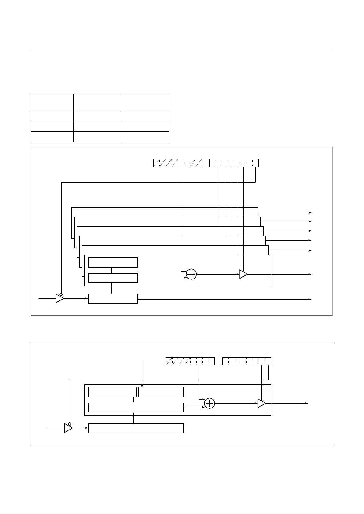
GMS81C4040/87C4060
PRELIMINARY
46
PRELIMINARY
Nov. 1999 Ver 1.0
14. Pulse Width Modulation (PWM)
The PWM circuit is shown in Figure 14-1 , Figure . The PWM circuit cons ists of the counter, comparator, Data
register.
The PWM control registers are PWMR7~0, PWMCR2~1,
PWM8H, PWM8L.
The more details about registers are shown Figur e 14-2 .
Figure 14-1 8bit register (PWM7~0) circui t
Figure 14-2 14bit re gister (PWM8) circuit
Example
(f
ex
=8MHz)
14bit PWM 8bit PWM
Resolution 0.5uS 4uS
Input Clock 2MHz 250KHz
Frame cycle 8,192uS 1,024uS
PWMCR2 [EBH]
8bit counter
PWM0
PWMCR1 [EAH]
8bit comparator
PWMR0 [E0H]
EN5
EN4
EN3
EN2
EN1
EN0
PWMR1 [E1H]
PWMR2 [E2
H
]
PWMR3 [E3
H
]
PWMR4 [E4
H
]
PWMR5 [E5
H
]
PWM5
PWM4
PWM3
PWM2
PWM1
IF1Frame
PS5
CNTB
PWMCR2 [EBH]
14bit counter
PWM8
PWMCR1 [EAH]
14bit comparator
PWMR8H 8bit [E8H]
EN8
PS2
CNTB
PWMR8L 6bit [E9H]
MSB LSB
Internal Control
Page 51
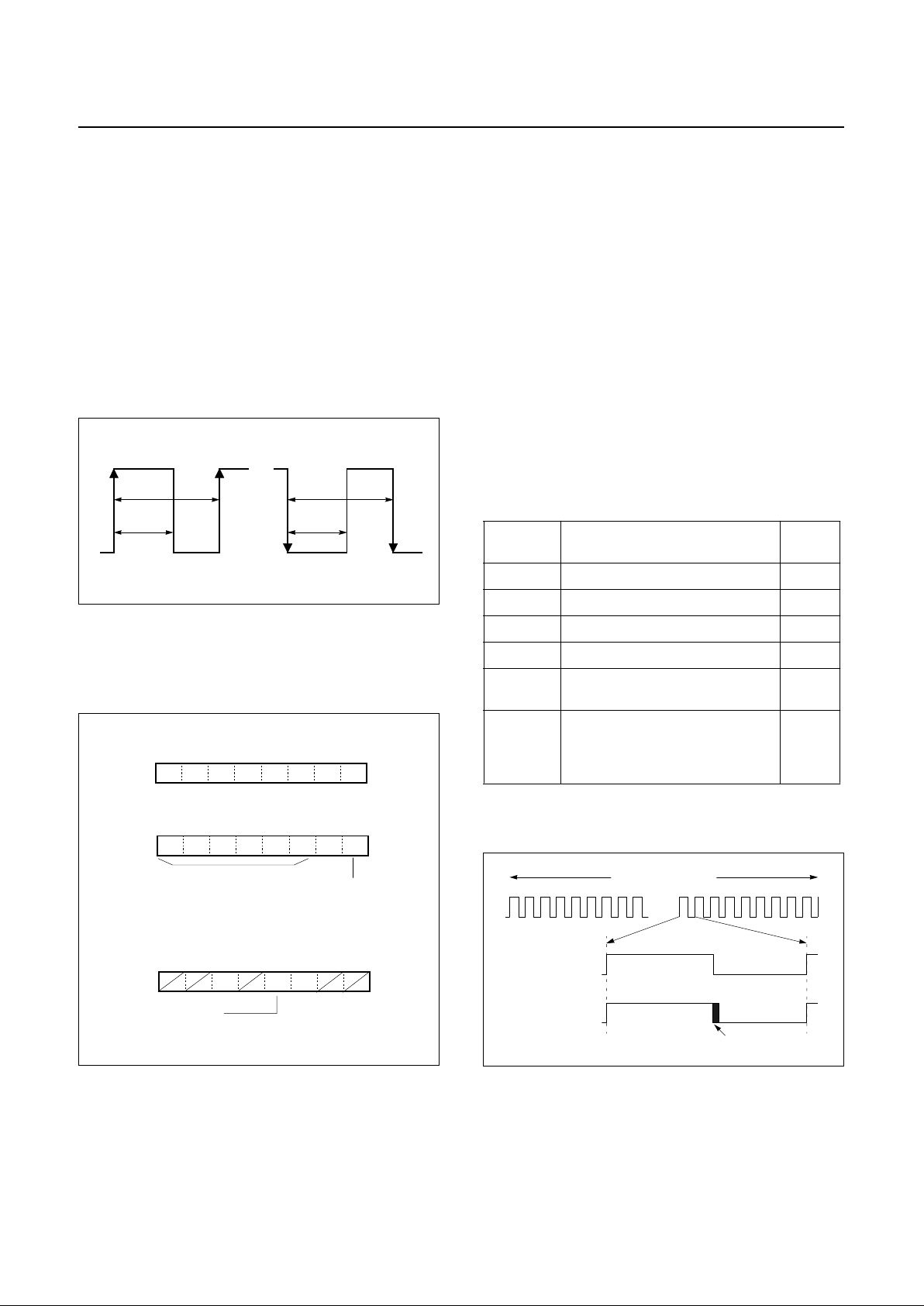
PRELIMINARY
GMS81C4040/87C4060
Nov. 1999 Ver 1.0
PRELIMINARY
47
8bit PWM Control
The GMS81C4040/GMS87C4060 contains a one 14bit
PWM and six 8bit PWM module.
1. 8bit PWM0~5 is wholy same internal circuit, but
PWM0~5 output port is NMOS open drain.
2. Al l PWM polarity has the same by POL2 ’s value.
3. Calulate Frame cycle and Pulse width is as following.
PWM Frame Cycle = 2
13
/ fex (Sec)
PWM Width = (PWMRn+1) * 2
5
/ fex (n=0~5)
Pulse Duty (%) = (PWMRn + 1) / 256 *100( %) (n=0~5)
Figure 14-3 Wave form exampl e for 8bit PWM
4. PWM outp ut is e nabled d uring E Nn(n=0 ~5) bit (See
PWMCR1~2) contain s 1.
Figure 14-4 8bit PWM Registers
5. CNTB controls all PWM counter enable.
If CNTB=0, Counter is enable d.
14bit PWM Control
1. 14bit PWM’s operation concept is not the same as 8bit
PWM.
1 PWM f r a m e c o nt ains 64 sub P W M s.
PWM8H : Set sub PWM’s basic Pulse Width.
PWM8L : Number of sub PWM which is added 1 clock.
2. PWM polarity is selected by POL1’s value.
If POL1=0, Positive Polarity.
3. Calulate Frame cycle and Pulse width is as following.
Main PWM Frame Cycle = 2
16
/ fex (Sec).
Sub PWM Frame Cycle = Main Frame Cycle / 64.
4. Table 14-1, “PWM8L and Sub frame matching table,”
on page 47 show PWM8L function.
Figure 14-5 Wave form example for 14bit PWM
Positive Polarity (POL2=0)
1
2
Negative Polarity (POL2=1)
1
2
1. Frame cycle
2. Pulse Width
PWM Data Register
PWMR0~5
ADDRESS : 0E0~E5
H
RESET VALUE : Undefined
D7 D6 D5 D4 D3 D2 D1 D0
EN5,4,3,2,1 : R47,45,43,42,41,40
PWM control Register 1
PWMCR1
ADDRESS : 0EA
H
RESET VALUE : 0000 0000
b
0: R4x acts normal digital port
1: R4x acts PWM output port
EN2 EN1 EN0 EN8 CNTBEN3EN4EN5
PWM control Register 2
PWMCR2
ADDRESS : 0EB
H
RESET VALUE : --0- 00--
b
POL2 POL1BUZS
8bit PWM Polarity
0: Positive (PWM from Rising edge)
1: Negative (PWM from Rising edge)
14bit Counter enable
0: Counter run
1: Counter stop
WWWWWWWW
RW RW RW RW RW RW RW RW
RW RW RW
Bit value
Sub frame number which is
added 1 clock
Pulse
count
if Bit0=1 32 1
if Bit1=1 16, 48 2
if Bit2=1 8, 24, 40, 56 4
if Bit3=1 4, 12, 20, 28, 36, 44, 52, 60 8
if Bit4=1
2, 6, 10, 14, 18, 22, 26, 30, 34,
38, 42, 46, 50, 54
16
if Bit5=1
1, 3, 5, 7, 9, 11, 13, 15, 17, 19,
21, 23, 25, 27, 29, 31, 33, 35, 37,
39, 41, 43, 45, 47, 49, 51, 53, 55,
57, 59, 61, 63
32
Table 14-1 PWM8L and Sub frame matching tabl e
Main PWM Frame
.....
012 616263
Sub PWM Frame
Sub PWM Frame
which is added
1 clock
1 clock width : PS2
Page 52
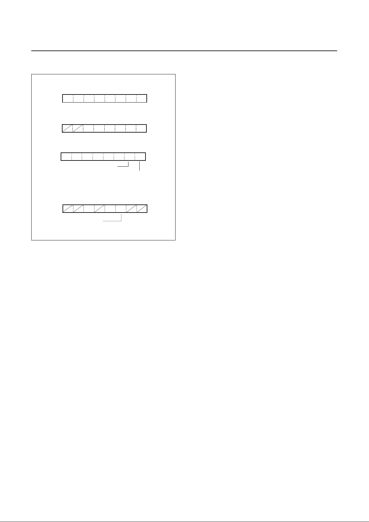
GMS81C4040/87C4060
PRELIMINARY
48
PRELIMINARY
Nov. 1999 Ver 1.0
Figure 14-6 14bit PWM Registers
5. PWM output is enabled during EN8 bit contains 1.
6. CNTB controls PWM counter enable.
If CNTB=0, Counter is enable d.
PWM Width Data Register
ADDRESS : 0E8
H
RESET VALUE : Undefined
D7 D6 D5 D4 D3 D2 D1 D0
PWM Sub-pulse count Register
PWM8L
ADDRESS : 0E9
H
RESET VALUE : Undefined
PWM c ontr ol Register 2
PWMCR2
ADDRESS : 0EB
H
RESET VALUE : --0- 00--
b
POL2 POL1BUZS
14bit PWM Polarity
0: Positive (PWM from Rising edge)
1: Negative (PWM from Rising edge)
PWM8H
D5 D4 D3 D2 D1 D0
PWM control Register 1
PWMCR1
ADDRESS : 0EA
H
RESET VALUE : 0000 0000
b
EN2
EN1 EN0 EN8 CNTBEN3EN4EN5
14bit Counter enable
0: Counter run
1: Counter stop
14bit PWM enable
0: R51
1: PWM8
RW RW RW RW RW RW RW RW
RW RW RW
RW RW RW RW RW
RW RW
RW
RW RW RW RW RW RW
Page 53
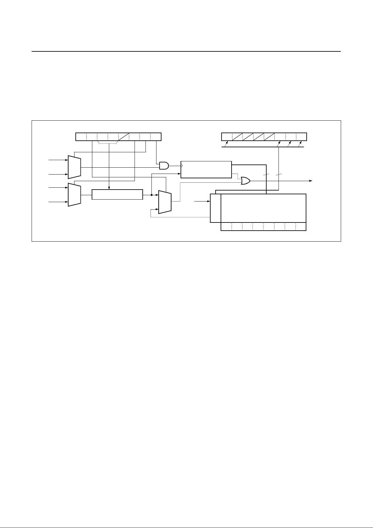
PRELIMINARY
GMS81C4040/87C4060
Nov. 1999 Ver 1.0
PRELIMINARY
49
15. Interrupt interval measurement circuit
The Interrupt interva l measurement circuit i s shown in Figure 15-1 .
The Interrupt interval measurement circuit consists of the
input multipl exer, sam pling cloc k multiple xer, Edge detec-
tor, 8bit co unter, me asured res ult stori ng registe r, FIFO
(9bit, 6level) interrupt, Control register, etc.
The more details about registers are shown Figur e 15-2 .
Figure 15-1 Block Dia gram of Interrupt interval measurement circuit
Control
The GMS81C4040/GMS87C4060 contains a Interrupt interval measurement module.
1. Select interrupt input pin what you want to measure by
set the FUNC1 [00CE
H
].
2. Set IDCR [00F9
H
] : FIFO clear, interrupt mode, interrupt edge select, external interrupt select between INT3
and INT4, sampling clock select.
3. Set IDCR [00F9
H
] : set IDST to star t measuring.
4. Counter value is stored to IDR [00FB
H
] when sele cted
edge is detected. After dat a was wri tten, timer is clea rd automatica lly and it counts continue.
5
. You can select interrupt occuring point by set Interrupt
Mode Select bit (IMS), every edge what you selected or
FIFO 4 level is filled.
6. If input signal’s int erval is larger than maximum counter
value (0FF
H
), counter occu rring an interrupt an d count
again from 00
H
.
7. See Figure 15-4 FIFO operating mechanism.
MUX
IDCR [F9H]
I34H I34L ISEL IDCK IDST
IDFS [FAH]
INT3
INT4
8bit counter
FIFO
(9bit, 6level)
INTV
IMS
1
0
DPOL FOE FFUL FEMPFCLR
MUX
PS8
PS9
1
0
MUX
0
1
Edge detector
Clear
IDR [FBH]
D7 D6 D5 D4 D3 D2 D1 D0
Overflow 8 4
FCLR
Page 54
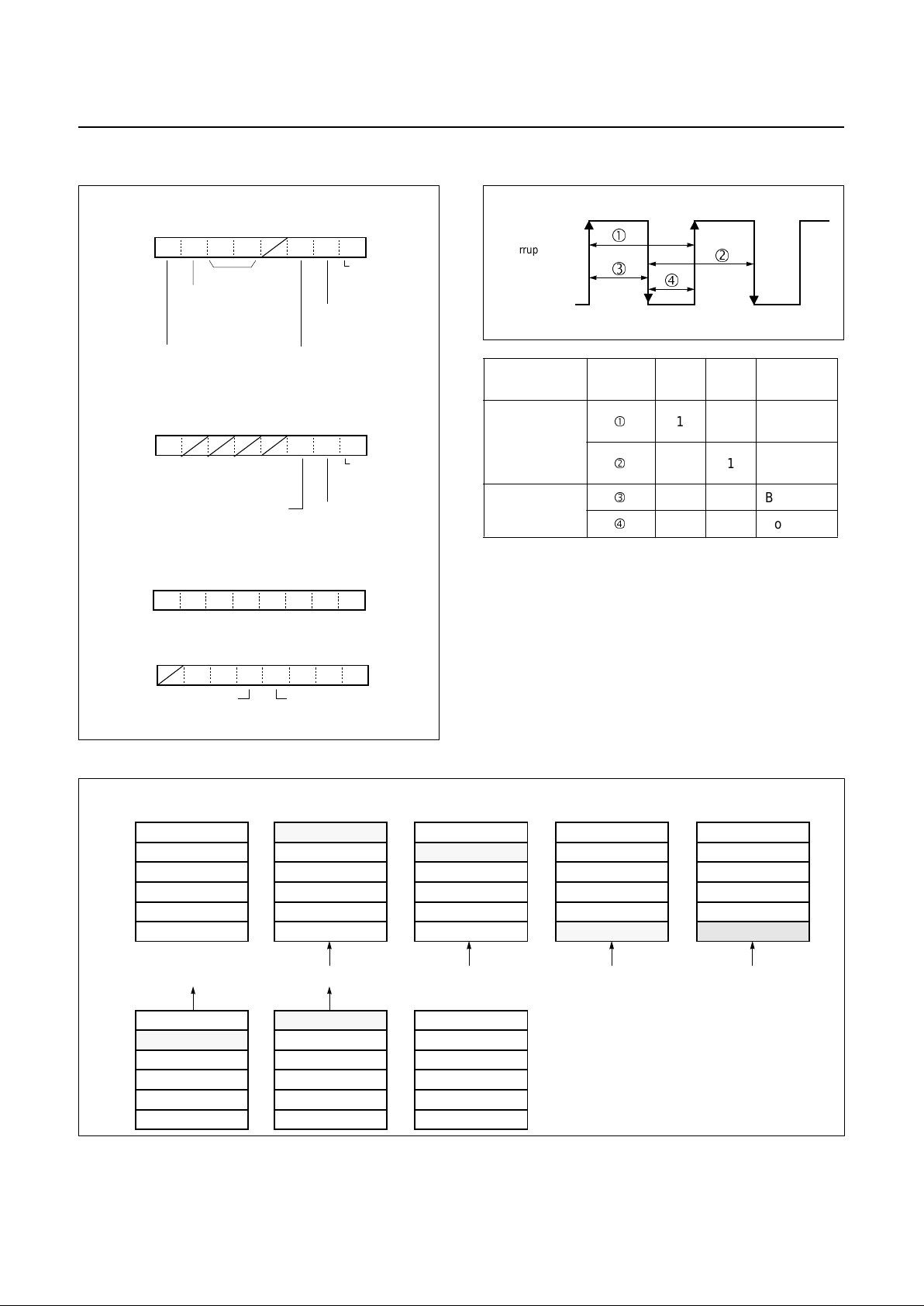
GMS81C4040/87C4060
PRELIMINARY
50
PRELIMINARY
Nov. 1999 Ver 1.0
Figure 15-2 Int. interval measurement Registers
Figure 15-3 Setting for measurement
Figure 15-4 Example for FIFO operating mechanism
IDR
ADDRESS : 00FB
H
RESET VALUE : Undefined
Interrupt interval determination
IDCR
ADDRESS : 00F9
H
RESET VALUE : 0000 -000
b
Counter control
0: stop
1: Clear & count
Sampling clock select
0: PS9
1: PS8
Int. occuring time
0: Every selected
I34H I34LFCLR ISEL IDCK IDSTIMS
See Figure 15-3
D7 D6 D5 D4 D3 D2 D1 D0
R24/INT3
Port function select Register 1
FUNC1
ADDRESS : 00CE
H
RESET VALUE : -000 0000
b
0: R24
1: INT3
INT4S INT3S INT2S INT1S INT0SEC2SEC3S
control Register
External Interrupt select
0: INT3
1: INT4
FIFO clear
0: Ignored
1: Clear and return to 0
edge by I34H/L
1: Every FIFO 4level
is filled
is filled
Interrupt interval determination
IDFS
ADDRESS : 00FA
H
RESET VALUE : 1--- -001
b
FIFO Empty flag
0: Data filled
1: Empty
FIFO Full flag
0: Not full
1: Full
DPOL FOE FFUL FEMP
FIFO status Register
FIFO overrun error flag
0: No Error
1: Error detected
Data polarity
0: Data is stored every Falling edge
Interrupt interval determination
FIFO Data Regi ster
1: Data is stored every Rising edge
R26/INT4
0: R26
1: INT4
RW RW RW RW
RW RW
RW
R RRR
RRRRRRRR
WWWWWWW
Item Symbol I34H I34L
Detecting
edge
Frame Cycle
10
Rising
edge
01
Falling
edge
Pulse width
1 1 Both edge
1 1 Both edge
Interrupt input
1) FIFO storing mechanism
2) FIFO reading mechanism
FEMP=1, FFUL=0 FEMP=0, FFUL=0 FEMP=0, FFUL=0 FEMP=0, FFUL=1 FEMP=0, FFUL=1
FEMP=0
FEMP=0 FEMP=1
Read out
Read out
Data in Data in Data in Data in
Data 6 will be erased.
Data 1 Data 1
Data 2
Data 1
Data 2
Data 3
Data 4
Data 5
Data 6
Data 1
Data 2
Data 2
Data 1
Data 2
Data 3
Data 4
Data 5
Data 7
FOE=1 (Over run error)
Page 55
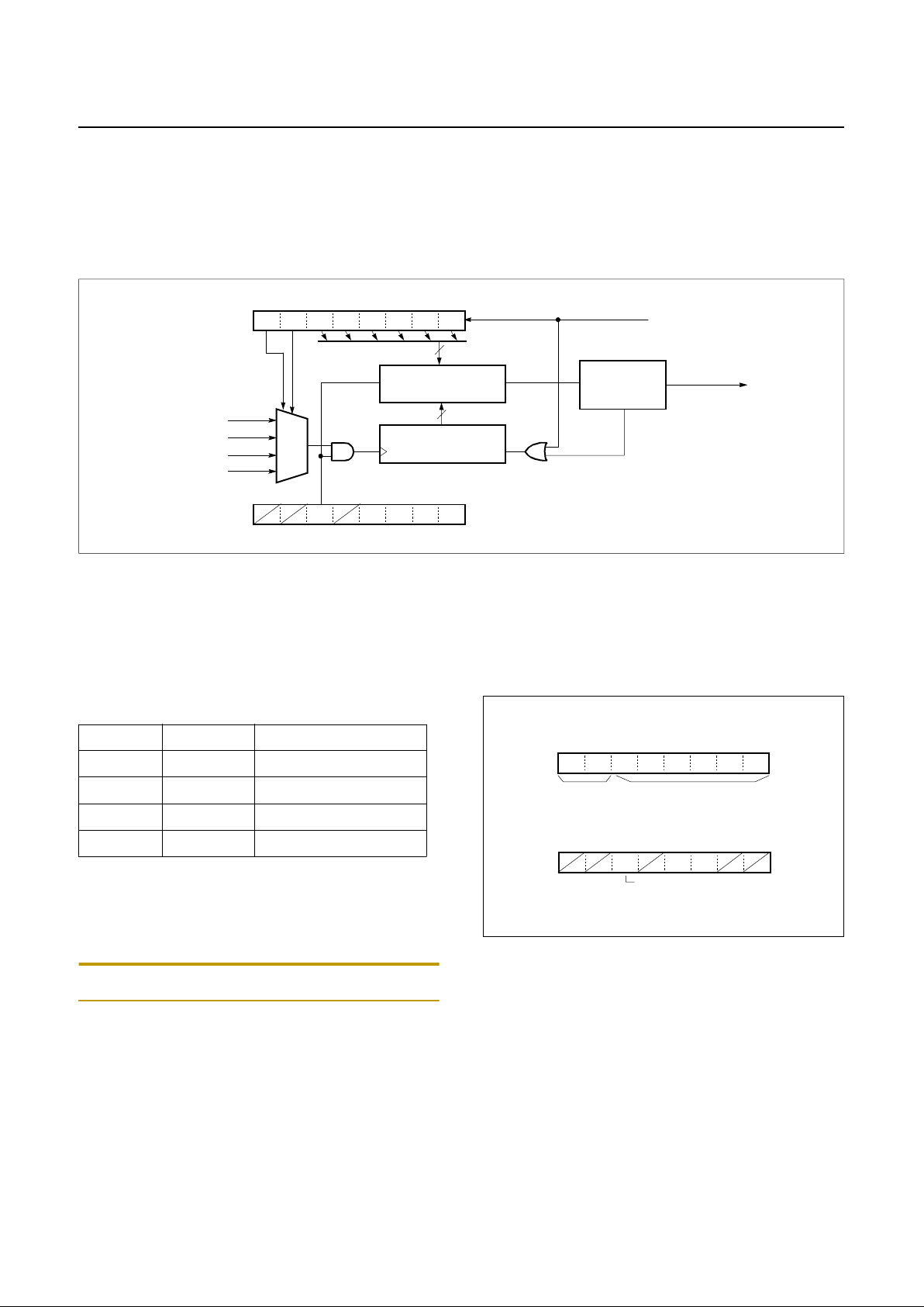
PRELIMINARY
GMS81C4040/87C4060
Nov. 1999 Ver 1.0
PRELIMINARY
51
16. Buzzer driver
The Buzzer driver circuit is shown in Figure 16-1 .
The Buzzer driver circuit consists of the 6bit counter, 6bit
comparator, Buzzer data register BUR(00EE
H
). The BUR
register control s source clock and output frequency.
The more details about registers are shown Figur e 16-2 .
Figure 16-1 Block Diag ram of Buzzer driver circuit
Control
The GMS81C4040/GMS87C4060 contains a Buzzer driver module.
1. Selec t an input clock among P S4~7 by set the
BUCK1~0 of BUR.
2. Select output frequency by change the BU5~0.
Output frequency = 1 / (PSx * BUy *2) Hz.
x=4~7, y=5~0
See example Table 16-1 and Table 16-2.
Note:
Do not select 00
H
to BU5~0. It means counter stop.
3. Set BUZS bit for output enable.
4. Output waveform is recta gle clo ck which has 50% duty.
5. You can use this clock for the other purposes.
Figure 16-2 Buzzer driver Registers
BUR [EEH]
BU5 BU4 BU3 BU2 BU1 BU0
6bit counter
Output
Generator
BUZZ
BUCK
MUX
PS4
PS6
PS5
PS7
BUCK
-1 -0
00
01
10
11
clear
6bit Comparator
clear
PWMCR2 [EBH]
BUZS POL2 POL1 EN7 EN6
BUR write
6
6
BUCK1 BUCK0 Clock source
0 0 PS4
0 1 PS5
1 0 PS6
1 1 PS7
Buzzer data Register
BUR
ADDRESS : 0EE
H
RESET VALUE : ???? ????
b
Input select
Clock Sel ect
PWM control Register 2
PWMCR2
ADDRESS : 0EB
H
RESET VALUE : --0- 00--
b
POL2 POL1BUZS
R50/Buzz select
0: R50
1: Buzz output
BU5 BU4 BU3 BU2 BU1 BU0
BUCKBUCK
-1 -0
WWWWWWWW
RW RW RW
Page 56
GMS81C4040/87C4060
PRELIMINARY
52
PRELIMINARY
Nov. 1999 Ver 1.0
BUR5~0 Output frequency (KHz)
Dec Hex PS4 PS5 PS6 PS7
1
2
3
4
5
6
7
8
9
10
11
12
13
14
15
16
17
18
19
20
21
22
23
24
25
26
27
28
29
30
31
32
33
34
35
36
37
38
39
40
41
42
43
44
45
46
47
48
49
50
51
52
53
54
55
56
57
58
59
60
61
62
63
01
02
03
04
05
06
07
08
09
0A
0B
0C
0D
0E
0F
10
11
12
13
14
15
16
17
18
19
1A
1B
1C
1D
1E
1F
20
21
22
23
24
25
26
27
28
29
2A
2B
2C
2D
2E
2F
30
31
32
33
34
35
36
37
38
39
3A
3B
3C
3D
3E
3F
250
125
83.333
62.5
50
41.666
35.714
31.25
27.728
25
22.728
20.834
19.23
17.858
16.666
15.626
14.706
13.888
13.158
12.5
11.904
11.364
10.87
10.416
10
9.616
9.26
8.928
8.62
8.334
8.064
7.812
7.576
7.352
7.124
6.944
6.756
6.578
6.41
6.25
6.098
5.952
5.814
5.682
5.556
5.434
5.32
5.208
5.102
5
4.902
4.808
4.716
4.63
4.546
4.464
4.386
4.31
4.238
4.166
4.098
4.032
3.968
125
62.5
42.666
31.25
25
20.888
17.858
15.625
13.888
12.5
11.364
10.417
9.615
8.929
8.333
7.813
7.353
6.944
6.579
6.25
5.952
5.682
5.435
5.208
5
4.808
4.63
4.464
4.31
4.167
4.032
3.906
3.788
3.676
3.571
3.472
3.378
3.289
3.205
3.125
3.049
2.976
2.907
2.841
2.778
2.717
2.66
2.604
2.551
2.5
2.451
2.404
2.358
2.315
2.273
2.232
2.193
2.155
2.119
2.083
2.049
2.016
1.984
62.5
31.25
20.833
15.625
12.5
10.461
8.928
7.813
6.944
6.25
5.682
5.209
4.808
4.484
4.166
3.906
3.676
3.472
3.289
3.125
2.976
2.841
2.718
2.604
2.5
2.404
2.315
2.232
2.155
2.084
2.016
1.953
1.894
1.838
1.786
1.736
1.689
1.645
1.602
1.563
1.524
1.488
1.453
1.421
1.389
1.359
1.33
1.302
1.276
1.25
1.225
1.202
1.179
1.157
1.136
1.116
1.096
1.078
1.059
1.042
1.025
1.008
0.992
31.25
15.625
10.436
7.813
6.25
5.208
4.464
3.907
3.472
3.125
2.841
2.604
2.404
2.242
2.083
1.953
1.838
1.736
1.644
1.562
1.438
1.420
1.359
1.302
1.25
1.202
1.158
1.116
1.078
1.042
1.008
0.976
0.947
0.919
0.893
0.868
0.845
0.822
0.801
0.781
0.762
0.744
0.727
0.710
0.694
0.679
0.665
0.651
0.638
0.625
0.613
0.601
0.590
0.579
0.568
0.558
0.548
0.539
0.530
0.521
0.512
0.504
0.496
Table 16-1 . Example for fex=8MHz
BUR5~0 Output frequency (KHz)
Dec Hex PS4 PS5 PS6 PS7
1
2
3
4
5
6
7
8
9
10
11
12
13
14
15
16
17
18
19
20
21
22
23
24
25
26
27
28
29
30
31
32
33
34
35
36
37
38
39
40
41
42
43
44
45
46
47
48
49
50
51
52
53
54
55
56
57
58
59
60
61
62
63
01
02
03
04
05
06
07
08
09
0A
0B
0C
0D
0E
0F
10
11
12
13
14
15
16
17
18
19
1A
1B
1C
1D
1E
1F
20
21
22
23
24
25
26
27
28
29
2A
2B
2C
2D
2E
2F
30
31
32
33
34
35
36
37
38
39
3A
3B
3C
3D
3E
3F
375
187.5
125
93.75
75
62.5
53.572
46.875
41.666
37.5
34.09
31.25
28.846
26.786
25
23.436
22.058
20.833
19.736
18.75
17.858
17.045
16.304
15.625
15
14.424
13.888
13.393
12.932
12.5
12.096
11.718
11.364
11.03
10.714
10.416
10.136
9.868
9.616
9.375
9.146
8.929
8.72
8.523
8.334
8.152
7.978
7.813
7.654
7.5
7.352
7.212
7.076
6.944
6.818
6.696
6.578
6.466
6.356
6.25
6.148
6.048
5.952
187.5
93.75
62.5
46.875
37.5
31.25
26.786
23.436
20.833
18.75
17.045
15.625
14.423
13.393
12.5
11.719
11.029
10.417
9.868
9.375
8.929
8.523
8.152
7.813
7.5
7.212
6.944
6.696
6.466
6.25
6.048
5.859
5.682
5.515
5.357
5.208
5.068
4.934
4.808
4.688
4.573
4.464
4.36
4.261
4.167
4.076
3.989
3.906
3.827
3.75
3.676
3.606
3.538
3.472
3.409
3.348
3.289
3.233
3.178
3.125
3.074
3.024
2.976
93.75
46.875
31.35
23.436
18.75
15.625
13.393
11.719
10.417
9.375
8.523
7.813
7.211
6.696
6.25
5.859
5.515
5.208
4.934
4.688
4.464
4.261
4.076
3.906
3.75
3.606
3.472
3.348
3.233
3.125
3.024
2.930
2.841
2.757
2.679
2.604
2.534
2.467
2.404
2.344
2.287
2.232
2.18
2.131
2.083
2.038
1.995
1.953
1.913
1.875
1.838
1.802
1.769
1.736
1.705
1.674
1.645
1.616
1.589
1.563
1.537
1.512
1.488
46.875
23.438
15.625
11.719
9.375
7.813
6.696
5.895
5.208
4.688
4.261
3.906
3.606
3.348
3.125
2.930
2.757
2.604
2.467
2.344
2.232
2.131
2.038
1.953
1.875
1.803
1.736
1.674
1.616
1.563
1.512
1.465
1.420
1.379
1.339
1.302
1.267
1.234
1.202
1.172
1.143
1.116
1.09
1.065
1.042
1.019
0.997
0.977
0.957
0.938
0.919
0.901
0.884
0.868
0.852
0.837
0.822
0.808
0.795
0.781
0.768
0.756
0.744
Table 16-2 . Example for fex=12MHz
Page 57
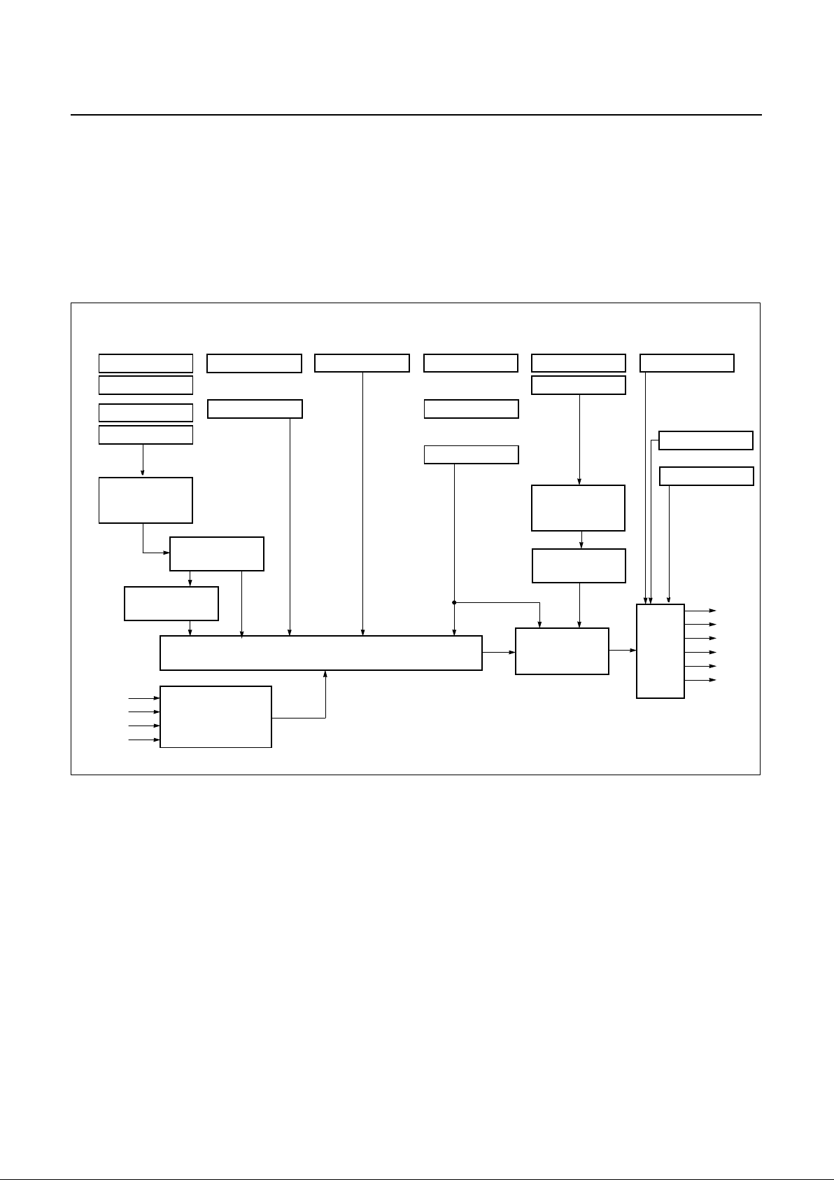
PRELIMINARY
GMS81C4040/87C4060
Nov. 1999 Ver 1.0
PRELIMINARY
53
17. On Screen Display (OSD)
The On Screen Display circuit is shown in Figure 17-1 .
The GMS81C4040/GM S87C4060 can support 5 12 OSD
chacters, but the last 6 characters (number 506 ~ 511,
1FA
H
~ 1FFH) are reserved for IC test a nd its pattern is
fixed by manufacturer. So you can use 506 characters for
your own.
The OSD circuit consists of the Position attribute register,
Line register, Full screen screen contr ol register, sprite
control register, sprite position reigster, I/O polarity register, sprite RAM, font ROM, VRAM, etc. The more details
about registers are shown Figure 17-2.
Figure 17-1 Block Diagram of On Screen Dis play circuit
L1ATTR [AF0H]
OSD Control
Circuit
OSDLN [AE5H] OSDCON1 [AE0H] O SDCON2 [AE1H] SPVPOS [AE8H] OSDPOL [AE2H]
Line 1,2 Attribute,
Position register
Line register
Full screen control
Sprite position register I/O polarity registerSprite control register
register
L1VPOS [AF1
H
]
L2ATTR [AF3H]
L2VPOS [AF4H]
SPHPOS [AE9H]
LHPOS [AE6H]
Horizontal position register
FDWSET [AE3
H
]
Field detection register
EDGECOL [AE4
H
]
Edge color register
VRAM
Font ROM
Sprite Control
Circuit
Sprite RAM
OSD, Sprite Generation Circuit
Sprite Control
Circuit
Output
Control
Circuit
Synchronization
Circuit
HSYNC
VSYNC
OSC1
OSC2
R
G
B
I
YS
YM
Color Mode Register
COLMOD [0AEF
H
]
Mesh Control Register
MESHCON [0AEB
H
]
Page 58
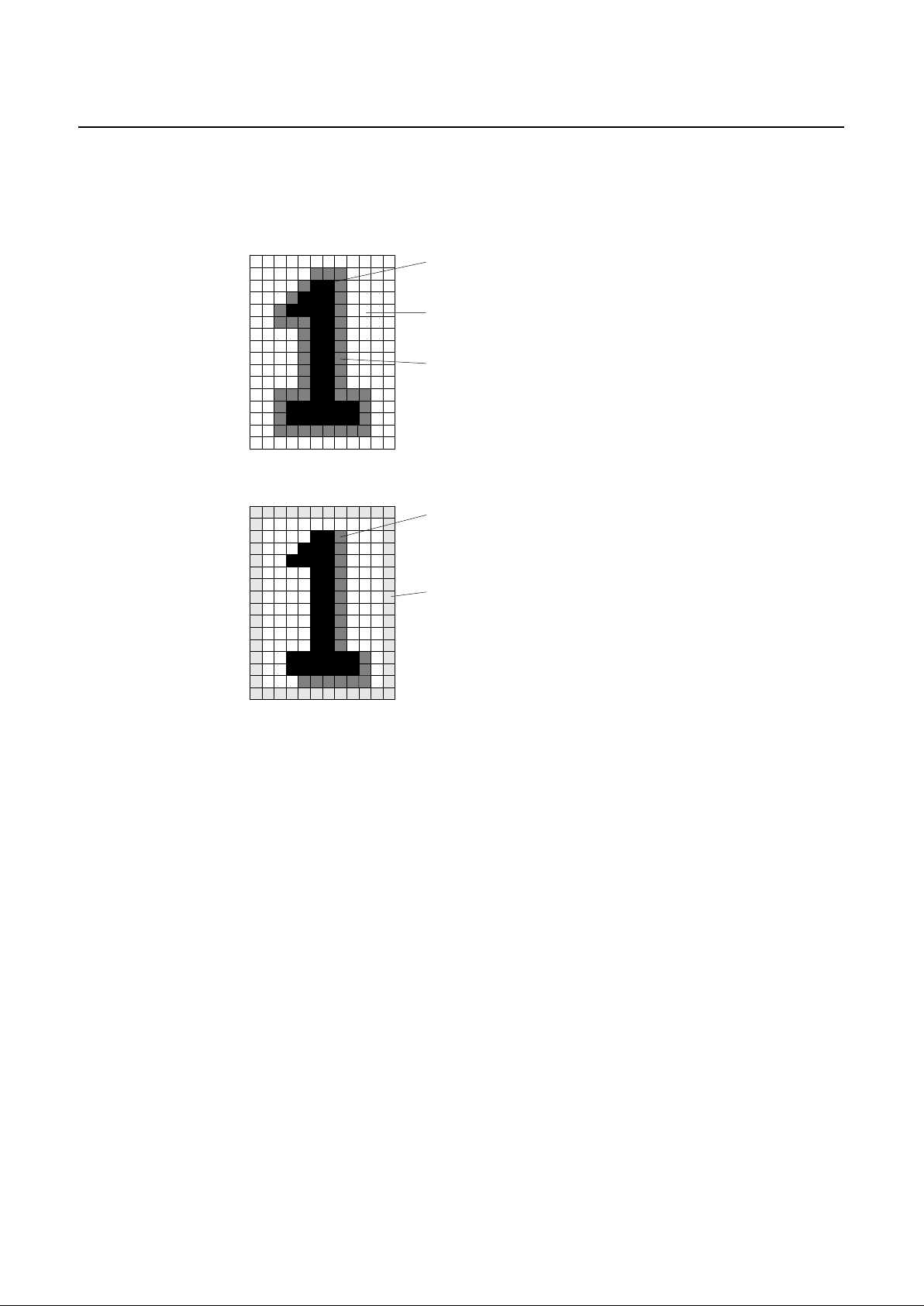
GMS81C4040/87C4060
PRELIMINARY
54
PRELIMINARY
Nov. 1999 Ver 1.0
Figure 17-2 OSD Character Font Example
Character(foreground)
Background
Characte(foreground) Outline
Character Shadow
Background Shadow
- 16 color with half intensity
- Color selecting: VRAM n-character bit19~16(see VRAM)
- 16 color with half intensity
- Color selecting :VRAM n-character bit23-20(see VRAM)
- Controled by LnATTR register(see LnATTR)
- 16 color with half intensity
- Color selecting : EDGECOL register(see EDGECOL)
- Controlled by VRAM n-character bit15-12
- Controlled by LnATTR register(see LnATTR) and
- Color selecting : EDGECOL register(see EDGECOL)
- 16 color with half intensity
VRAM n-character bit11-10(see VRAM)
- Color selecting : EDGECOL(see EDGECOL)
- 16 color with half intensity
(No Character Outline Case)
Page 59
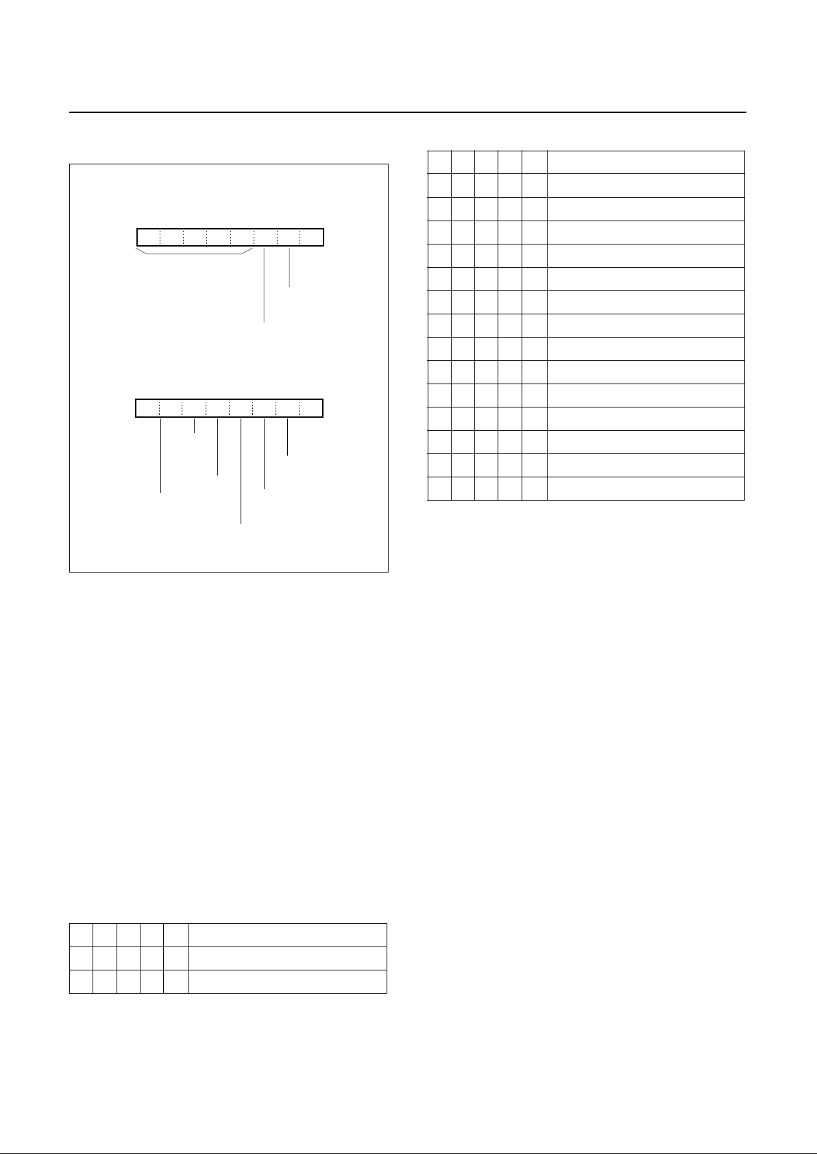
PRELIMINARY
GMS81C4040/87C4060
Nov. 1999 Ver 1.0
PRELIMINARY
55
Figure 17-3 OSD Control Registers - 1
OSDCON1
bit 0: STOCK
It contr ols OSD LC oscil lation. If os cillation is s toped,
IC’s power consumptio n is decreased.
bit 1: DDCLK
If you set this bit to 1, OSD input cl ock is doubled from LC
oscillation. It makes OSD horisontal image size as doubled.
bit 2: DLINE
If you s et this bit to 1, OSD vertical scan co unter input
clock is doubled from normal state. It makes OSD vertical
imag e siz e as d ou b l ed .
bit 7~3: FULLM, I, B, G, R
It controls back ground color as bel ow.
OSDCON2
bit 0: OSDON
It controls OSD, Sprite , Full s cree n backgr ound a t once. It
does not affect a nything t o Vsync in terrupt and OSD int errupt, etc.
bit 1: PROSD
It controls screen output priority between sprite and OSD.
If its value is 1, OSD hide sprit e patte rn in overa pped area .
bit 2: ENSP
It enables sprite display.
bit 3: DUSP
It doubles sprite’s horizontal & vertical size during this
value is 1.
bit 4: ONL1
It enables OSD line 1 display. If it is enabled, OSD inter-
rupt is activated.
bit 5: ONL2
It enables OSD line 2 display. If it is enabled, OSD inter-
rupt is activated.
bit 6: OBGW
It controls character’s width. Default width is 12dots. If its
value is set, 2 dots (background color) are added both left
M I B G R Color
0 0 0 0 0 Transparent (Normal TV)
00001 RED
Table 17-1 Full Screen Back ground color selection
Sprite OSD control Register
OSDCON2
ADDRESS : 0AE1
H
RESET VALUE : 0000 0000
b
Full screen control Register
OSDCON1
ADDRESS : 0AE0
H
RESET VALUE : 0000 0000
b
STOP OSD clock
0: Release
1: Stop
FULB FULG FULR DLINE DDCLK STOCKFULI
OBGW ONL2 ONL1 DUSP ENSP
PRO OSD
FULM
Double dot clock mode
0: Normal
1: Double
Double scan line mode
0: Normal
1: Double
Full screen background
FULLM
FULLI
FULLB
FULLG
FULLR
: Half blank
: Half intensity
: Blue
: Green
: Red
OSD, Sprite
0: All Off
1: All On
Priority
0: Sprite > OSD
1: OSD > Sprite
Sprite enable
0: Disable
1: Enable
Sprite size
0: Normal
1: Double
Background width
0: 12dots
1: 14dots
OSD line 2
0: Off
1: On
OSD line 1
0: Off
1: On
per 1 character
RW RW RW RW RW RW RW RW
RW RW RW RW RW RW RW
DUSP
CL
RW
SD ON
Double sprite
dot clock
(Sprite size)
0: x1, x2
1: x2, x4
00010 GREEN
0 0 0 1 1 RED+GREEN
0 0 1 0 0 BLUE
0 0 1 0 1 BLUE+RED
0 0 1 1 0 BLUE+GREEN
0 0 1 1 1 RED+GREEN+BLUE (WHITE)
0 1 0 0 0 BLACK
0 1 0 0 1 Half intensity RED
0 1 0 1 0 Half intensity GREEN
0 1 0 1 1 Half intencity RED+GREEN
0 1 1 0 0 Half intensity BLUE
0 1 1 0 1 Half intensity GREEN+BLUE
0 1 1 1 1 Half intensity WHITE
1 0 0 0 0 Half BLANK
M I B G R Color
Table 17-1 Full Scre en Back ground color selection
Page 60
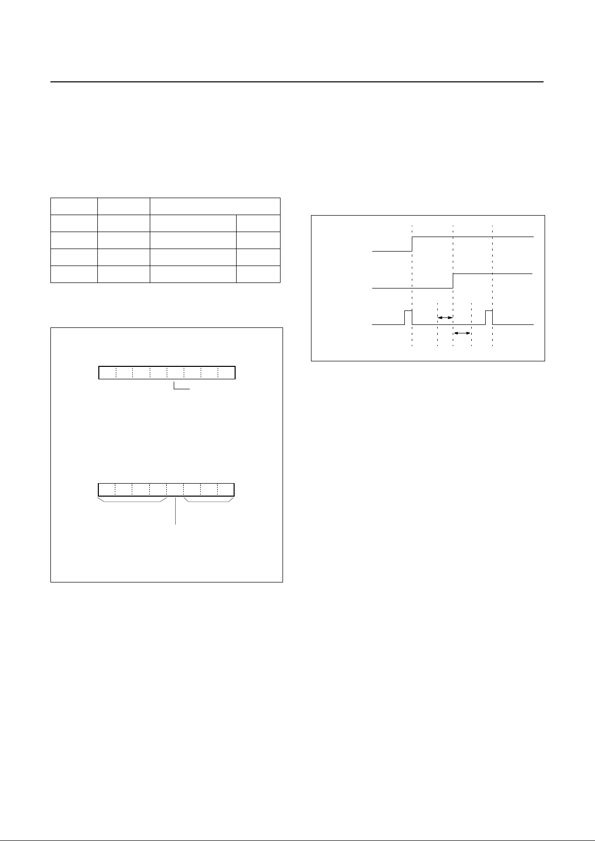
GMS81C4040/87C4060
PRELIMINARY
56
PRELIMINARY
Nov. 1999 Ver 1.0
and right side of character.
bit 7: DUSPCL
It controls spri te’s dot clock an d scan line speed. It d oes not
affect t o O SD. Sprite size is controlled as b elow.
Figure 17-4 OSD Registers - 2
OSDPOL
bit7~0 : POL HS, VS, I, YM, YS, B, G, R
It controls HS, VS, I, YM, YS, B, G, R port’s polarity. If
its value is 1, polarity is active high.
FDWSET
FDWSET (Field D etection Window Seting) register detects the begin of VSync(Vertical Sync.) signal and distinguishs its current field is Even field or Odd field.
Figure 17-5 FDWSET detection region
The region of FMIN[2:0] ~ FMAX[3:0] is field detection
window.
FMAX[3:0] can divide the region between HSyn c(Horizontal Sync.) by 16. You can assum e there i s 4 bit horizontal counter, for example HCOUNT[3:0] whic h count 0~15.
If the start of VSync is detected at the window, next field
is even. Else if VSync is detected another region of the
window, next field is odd.
It means start of VSync is detected dur ing FMIN[2:0 ] <
HCOUNT[3:0] < FMAX[3:0] and FPOL value is 0, it distinguish odd field.
And, star t of VSync is detected du ring FMIN[2: 0] <
HCOUNT[3:0] < FMAX[3:0] and FPOL value is 1, it distinguish even field.
FMIN[ 2 :0 ] , FM A X [ 3 : 0] ar e compar ed w it h th e h ori zo n ta l
counter in OSD block.
DUSPCL DUSP Size
0 0 Normal 12x16
0 1 x 2 24x32
1 0 Not used 1 1 x 4 48x64
Table 17-2 Sprite pattern size
I/O Polarity ( initial ) Register
OSDPOL
ADDRESS : 0AE2
H
RESET VALUE : Undefined
POL
POLI
POL
POL
POLB POLG
POLR
POL
YS
YMVSHS
0: Active Low
1: Active High
OSD display enable,POLHS
POLVS
POLI
POLYM
POLB
POLG
POLR
: Hsync. input
: Vsync. input
: Half intensity output
: Half blank output
: Blue output
: Green output
: Red output
include the edge color.
0: Off
1: On
Field detection Register
FDWSET
ADDRESS : 0AE3
H
RESET VALUE : 0111 1010
b
FPOL
FMIN2 ~ 0
FMAX3 ~ 0
Field detection polarity
0: Detect Odd field
Field detection
Maximum pointer
Field detection
Minimum pointer
Masking range : Min.~Max.
1: Detect Even field
Detecting range : Min.~Max.
WWWWWWWW
WWWWWWWW
HSync
Ex1: VSync(Odd)
Ex2: VSync(Even)
FMIN
FMAX
Page 61
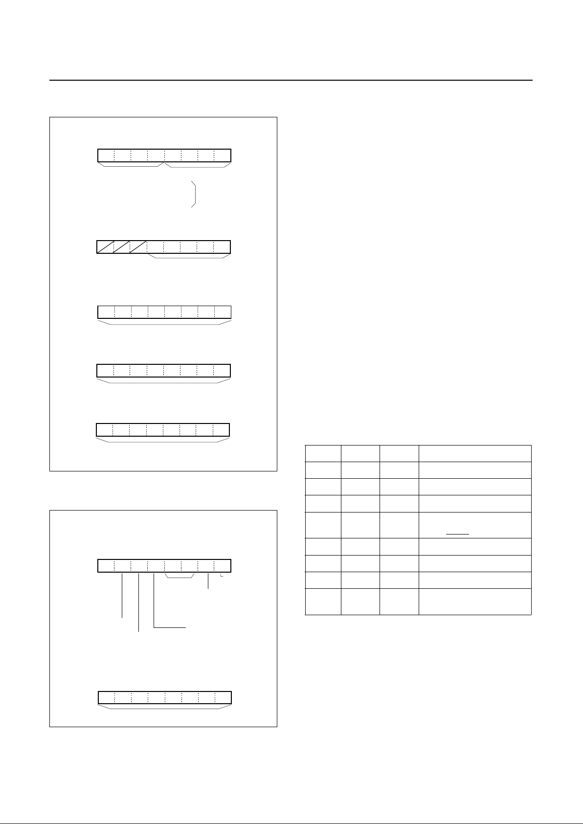
PRELIMINARY
GMS81C4040/87C4060
Nov. 1999 Ver 1.0
PRELIMINARY
57
Figure 17-6 OSD Registers - 3
Figure 17-7 OSD Registers - 4
L1ATTR
bit 0 : LIV8
It is equivalent with L1VPOS’s bit 8. See more details in
L1VPOS.
bit 1: FSC1
It selects charact er outline and shadow color. If it is 1, it se-
lect EDGE2 color in EDGECOL register. Or not, it select
EDGE1 color. According to EDGECOL register and this
bit character and shadow colors are selected simulteneously
bit 3~2: CSZ11~CSZ10
It controls OSD character’s size ( x1 , x2, x3). You can use
this register and DDCLK, DLINE bit, horizontal / vertical
size can be controlled (x2, x4, x6).
bit 4: ENSH1
It enables line 1’s character(fore ground) shadow.
bit 5: ENOL1
It enables line 1’s cha r acter(foreground) outline.
bit 6: WDSL1
It shows thickness of line 1’s shadow and outline.
bit 7: OBGH1
It controls character’s height. Default height is 16dots. If
its value is set, 2 dots (background color) are added both
top and bottom side of character.
OSD line Register
OSDLN
ADDRESS : 0AE5
H
RESET VALUE : ---0 0000
b
Background shadow / edge
EDGECOL
ADDRESS : 0AE4
H
RESET VALUE : Undefined
EDGnI
EDG
Edge 2 color
VLR4 ~ 0
color Register
2I
EDG2BEDG2GEDG2REDG
1I
EDG1GEDG
1R
EDG
1B
Edge 1 color
EDGnB
EDGnG
EDGnR
: Half Intensity
: Blue
: Green
: Red
n : 1 ~ 2
Current displayed OSD line number
( 00000 ~ 11111
b
: 0 ~ 63 )
OSD line horizontal
LHPOS
ADDRESS : 0AE6
H
RESET VALUE : Undefined
OSD line’s horizontal position (00 ~ FFH)
Sprite vertical
SPVPOS
ADDRESS : 0AE8
H
RESET VALUE : Undefiend
Sprite horisontal
SPHPOS
ADDRESS : 0AE9
H
RESET VALUE : Undefined
position Register
position Register
position Register
D7
D6 D5 D4 D3 D2 D1 D0
D7
D6 D5 D4 D3 D2 D1 D0
D7 D6 D5 D4 D3 D2 D1 D0
Sprite’s vertical position (00 ~ FFH)
Sprite’s horisontal position (00 ~ FF
H
)
WWWWWWWW
RRRRR
WWWWWWWW
WWWWWWWW
WWWWWWWW
OSD line 1’s
L1VPOS
ADDRESS : 0AF1
H
RESET VALUE : Undefined
OSD line 1’s
L1ATTR
ADDRESS : 0AF0
H
RESET VALUE : Undefined
Vertical position
Foreground shadow
ENOL ENSH C SZ CSZ
FSC1 L1V8
WDSL
Character size
L1V7 L1V6 L1V5 L1V4 L1V3 L1V2 L1V1 L1V0
attribute Register
vertical position Register
OSD line 1’s vertical position (include L1V8 : 000 ~ 1FFH)
OBGH
111111
10
L1VPOS’s bit8
out line color
0: Edge 1’s color
1: Edge 2’s color
00: Normal
01: 2 times
10: 3 times
11: Reserved
Character Shodow
0: Disable
1: Enable
charcater outline
0: Disable
1: Enable
Shadow / Outline
0: 1dot
1: Propotional
Character
0: 16dots
1: 18dots
background
height
width
to character
size
WWWWWWWW
WWWWWWWW
control
control
WDSL ENOL ENSH outline, shadow
0 0 0 No outline, No shadow
0 0 1 Thin shadow
0 1 0 Thin outline
011
Thin outline
Thick
shadow
1 0 0 No outline, No shadow
1 0 1 Thick shadow
1 1 0 Thick outline
111
Thick outline
Thick shadow
Table 17-3 Character Outl ine, Shadow table
Page 62
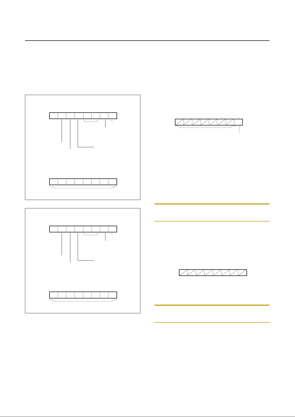
GMS81C4040/87C4060
PRELIMINARY
58
PRELIMINARY
Nov. 1999 Ver 1.0
L1VPOS
It shows OSD line 1’s vertical position in 9bit format
(LIV8 + L1VPOS, 000 ~ 1FF
H
).
Figure 17-8 OSD Registers - 5
Figure 17-9 OSD Register - 6
L2ATTR
It controls OSD line 2’ s attributes. Its function is the same
as L1ATTR.
L2VPOS
It shows OSD line 2’s vertical position. Its function is the
same as L1VPOS.
COLMOD
It controls OSD output m ode-RGB direct half intencity.
Figure 17-10 OSD Register - 7
bit 0: C16EN
It ena b les RG B p o r t h a l f in tenci ty ou tput. W hen this bi t is
set, RGB port gener at es hal f intenc it y output. Hal f int encity output is 3.5V voltage level output of RGB port. When
you use this bit, you must fill all the other bit with ‘0’.
Note:
When you do not use RGB direct half intncsity out-
put , please initi alize this register as 00h.
MESHCON
It controls OSD mesh mode color.
Figure 17-11 OSD Register - 8
Note:
Please ini tialize this re gister as 00h. Though thi s
register is for mesh mode color, it is not used currently.
VRAM
VRAM contains 1 OSD line, 24 character’s attributes.
Each character’s attribute is constructed with 3 bytes, it
contains color data for backgro und, shadow, outline, character and character number ( 000
H
~ 1FFH, 512 characters
OSD line 2’s
L2VPOS
ADDRESS : 0AF4
H
RESET VALUE : Undefined
OSD line 2’s
L2ATTR
ADDRESS : 0AF3
H
RESET VALUE : Undefined
Vertical position
Foreground shadow
ENOL ENSH C SZ CSZ
FSC2 L2V8
WDSL
Character size
L2V7L2V6L2V5L2V4L2V3L2V2L2V1L2V0
attribute Register
vertical position Register
OSD line 2’s vertical position (include L2V8 : 000 ~ 1FFH)
OBGH
22222120
L2VPOS’s bit8
out line color
0: Edge 1’s color
1: Edge 2’s color
00: Normal
01: 2 times
10: 3 times
11: Reserved
Shodow control
0: Disable
1: Enable
Out line control
0: Disable
1: Enable
Shadow / Outline
0: 1dot
1: Propotional
Character
0: 16dots
1: 18dots
background
height
width
to character
size
WWWWWWWW
WWWWWWWW
OSD line 2’s
L2VPOS
ADDRESS : 0AF4
H
RESET VALUE : Undefined
OSD line 2’s
L2ATTR
ADDRESS : 0AF3
H
RESET VALUE : Undefined
Vertical position
Foreground shadow
ENOL ENSH C SZ CSZ
FSC2 L2V8
WDSL
Character size
L2V7L2V6L2V5L2V4L2V3L2V2L2V1L2V0
attribute Register
vertical position Register
OSD line 2’s vertical position (include L2V8 : 000 ~ 1FFH)
OBGH
22222120
L2VPOS’s bit8
out line color
0: Edge 1’s color
1: Edge 2’s color
00: Normal
01: 2 times
10: 3 times
11: Reserved
Shodow control
0: Disable
1: Enable
Out line control
0: Disable
1: Enable
Shadow / Outline
0: 1dot
1: Propotional
Character
0: 16dots
1: 18dots
background
height
width
to character
size
WWWWWWWW
W
WWWW
WWW
Color Output Mode
COLMOD
ADDRESS : 0AEF
H
RESET VALUE : Undifined
RGB Half intensity enable
C16EN
Register
W
1: Enable
0: Enable
(see Note)
Fill with ‘0’
Mesh Mode Color
MESHCON
ADDRESS : 0AEB
H
RESET VALUE : See Note
Register
Page 63
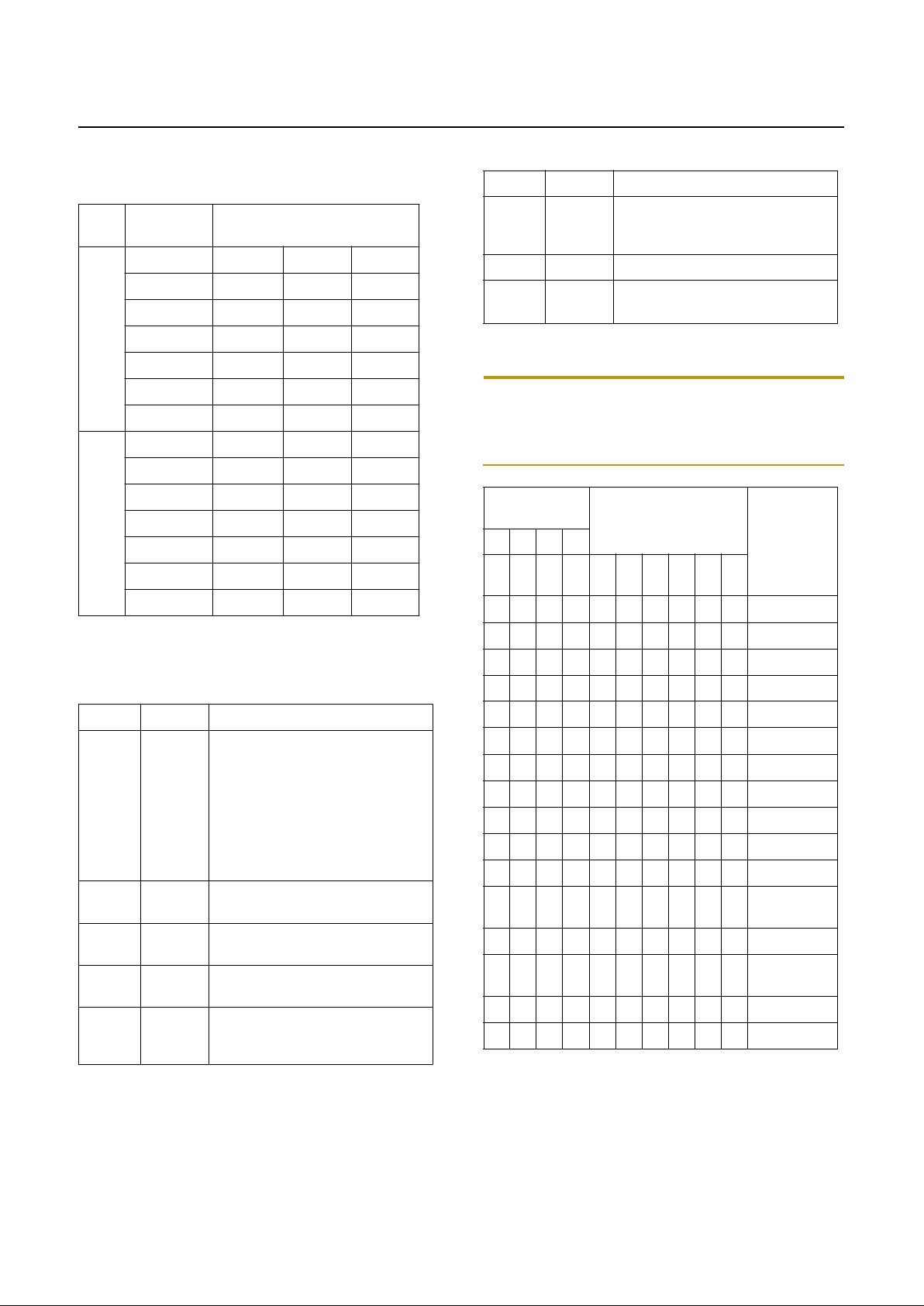
PRELIMINARY
GMS81C4040/87C4060
Nov. 1999 Ver 1.0
PRELIMINARY
59
), etc.
Note:
if (BSL = 1) & (BSCUL = 0) & (LnATTR,ENSHn = 1),
then the right bottom shadow of font character is shifted to
1 dot right side. This shadow effect will continue until that
(BSR) of adjacent charac ter attri buti on become (BSR = 1).
Line
No.
Character
No.
Address (bit 23~0)
Hexa decimal
1
1 A40 A20 A00
2 A41 A21 A01
3 A42 A22 A02
::::
22 A55 A35 A15
23 A56 A36 A16
24 A57 A37 A17
2
1 AC0 AA0 A80
2 AC1 AA1 A81
3 AC2 AA2 A82
::::
22 AD5 AB5 A95
23 AD6 AB6 A96
24 AD7 AB7 A97
Table 17-4 VRAM memory map
Bit No. Name Function
15 BSR
Enable right side background
shadow.
cf
. If BSL=1 and BSCUL=1 and
LnATTR.ENSHn=1, character’s
right bottom shadow is shifted to
right side by 1dot unit.
It acts continued until current
character’s r ight side chacter’ s
BSR is set to 1.
14 BSL
Enable left side background
shadow.
13 BSD
Enable bottom side backg round
shadow.
12 BSU
Enable top side background
shadow.
11 BSCDR
Select color of right and bo ttom
side shadow of the background
0: Edge1, 1: Edge2 color
Table 17-5 VRAM (bit15~0) funct ion
10 BSCUL
Select color of left and top side
shadow of the background
0: Edge1, 1: Edge2 color
9 ENRND Enable character’s rounding
8~0 CG8~0
Character font numb er
( among 000 ~ 1FF
H
)
Bit No. &
Name
Output ( Po larity :
Through)
Character
color
19 18 17 16
IBGR
YMY
S
IBGR
0000000000 Clear
0001010001 Red
0010010010 Green
0011010011 Yellow
0100010100 Blue
0101010101 Magenta
0110010110 Cyan
0111010111 White
1000010000 Black
1001010001 Half-I,Red
1010010010Half-I,Green
1011010011
Half-I,
Yellow
1100010100Half-I,Blue
1101010101
Half-I,
Magenta
1110010110Half-I,Cyan
1111010111Half-I,White
Table 17-6 VRAM (bit19~16) function
Bit No. Name Function
Table 17-5 VRAM (bit15~0) function
Page 64
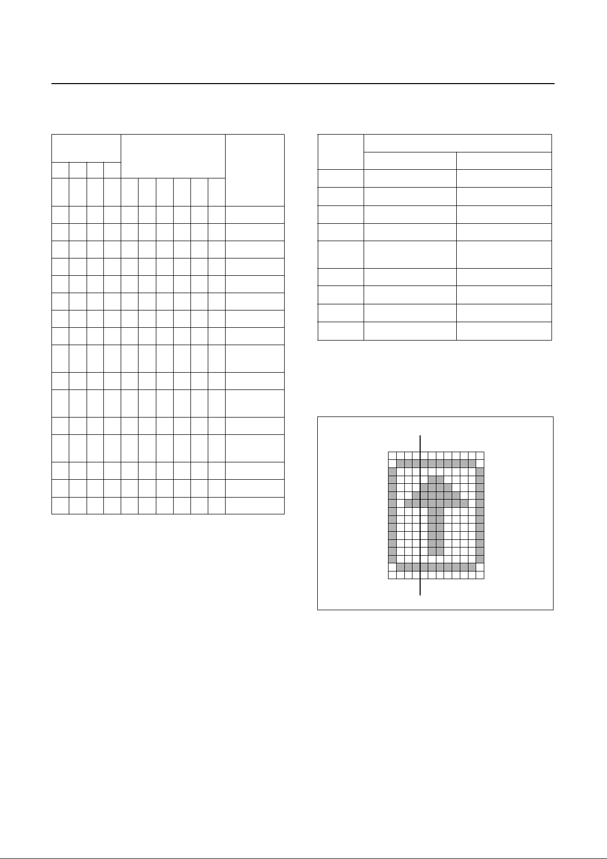
GMS81C4040/87C4060
PRELIMINARY
60
PRELIMINARY
Nov. 1999 Ver 1.0
Font ROM
The GMS81C4040/GMS 87C4060 OSD cha racter size is
fixed as 12dots (Horisontal) * 16dots (Vertical).
1. Each horisontal data (12dots) needs 2byte ROM.
2. One character is constructed with 16 horisontal data to
vertically. As a result, one chara cter needs 32bytes (2 * 16
bytes).
3. GMS81C4040/GMS87C4060 contains 512 characters.
Total Font ROM memory s ize is calu lated as 16,3 84bytes
( 32bytes / character * 512 character )
4. Font ROM memory is located from 10000
H
~ 13FFFH,
this memory can not be accessed by user program.
5. A character’s address and dot position in font ROM is
described in Figure 17- 12 .
Figure 17-12 Example for a character (53H)
Sprite RAM
The GMS81 C4040/GMS87 C4060 contains a 32b ytes
(12dot * 16dot) sprite RAM.
1. In view point, sprite is similar to character font but it is
not using font ROM.
2. You can selct color by dot unit.
3. Using above 1 an d 2, you c an mak e any of pa ttern s what
you want by software. For example, ar row cursor or some-
Bit No. &
Name
Output ( Po larity :
Through)
Back
ground
color
23 22 21 20
IBGR
YMY
S
IBGR
0000000000 Clear
0001010001 Red
0010010010 Green
0011010011 Yellow
0100010100 Blue
0101010101 Magenta
0110010110 Cyan
0111010111 White
1000100000
Half
blanking
1001011001Half-I,Green
1010011010
Half-I,
Yellow
1011011011Half-I,Blue
1100011100
Half-I,
Magenta
1101011101Half-I,Cyan
1110011110Half-I,White
1111010111 Black
Table 17-7 VRAM (bit 23 ~ 20) function
Charact
er code
Address range
Upper 4bit Lower 8bit
000
H
12000H ~ 1200F
H
10000H ~ 1000F
H
001
H
12010H ~ 1201F
H
10010H ~ 1001F
H
002
H
12020H ~ 1202F
H
10020H ~ 1002F
H
:: :
xyz
H
(12000H + xyz0H) ~
(12000H + xyzFH)
(10000H + xyz0H) ~
(10000H + xyzFH)
:: :
1FD
H
13FD0H ~ 13FDF
H
11FD0H ~ 11FDF
H
1FE
H
13FE0H ~ 13FEF
H
11FE0H ~ 11FEF
H
1FF
H
13FF0H ~ 13FFF
H
11FF0H ~ 11FFF
H
Table 17-8 Font ROM memory map
MSB LSB
Address
12530
H
12531
H
12532
H
12533
H
12534
H
12535
H
12536
H
12537
H
12538
H
12539
H
1253A
H
1253B
H
1253C
H
1253D
H
1253E
H
1253F
H
00
H
07
H
08
H
08
H
08
H
09
H
0B
H
08
H
08
H
08
H
08
H
08
H
08
H
08
H
07
H
00
H
Data Address
10530
H
10531
H
10532
H
10533
H
10534
H
10535
H
10536
H
10537
H
10538
H
10539
H
1053A
H
1053B
H
1053C
H
1053D
H
1053E
H
1053F
H
00
H
FE
H
01
H
61
H
F1
H
F9
H
FD
H
61
H
61
H
61
H
61
H
61
H
61
H
01
H
FE
H
00
H
Data
Page 65
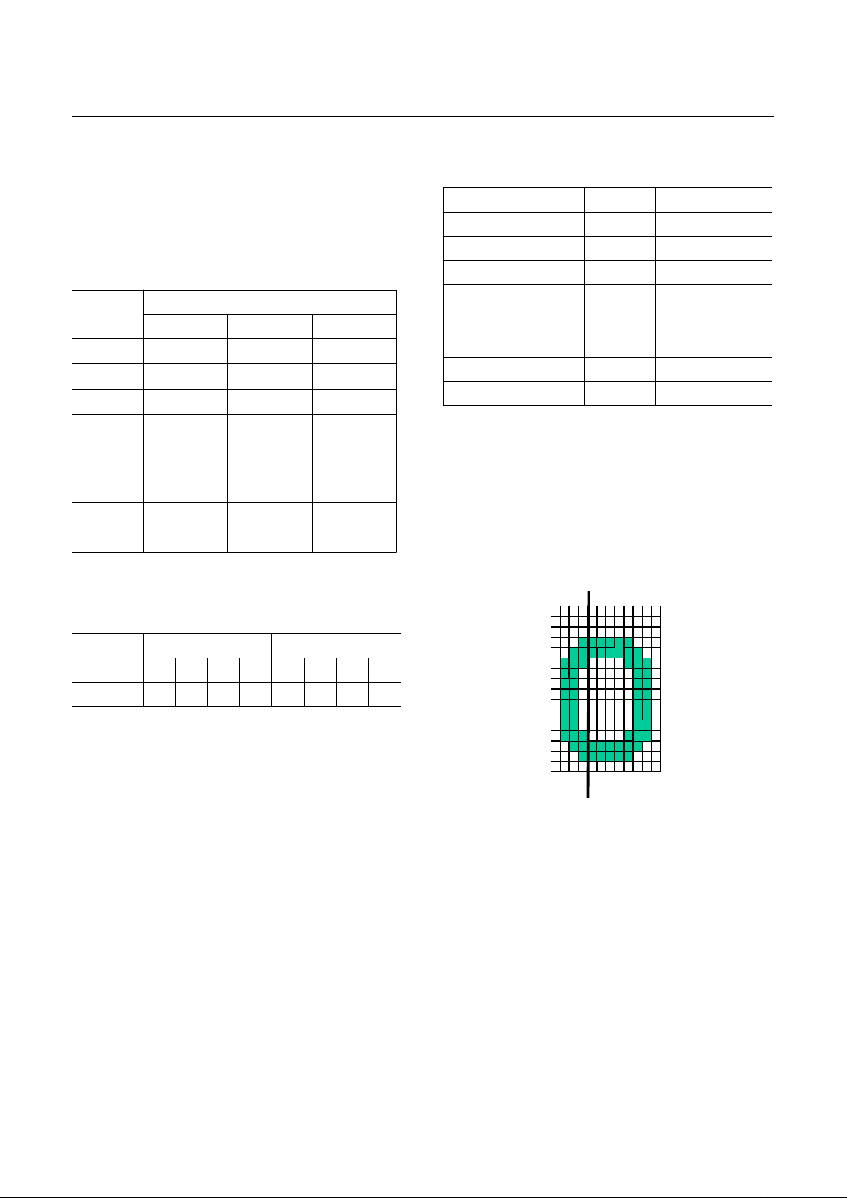
PRELIMINARY
GMS81C4040/87C4060
Nov. 1999 Ver 1.0
PRELIMINARY
61
thing.
4. Sprite position is controlled by sprite position register
SPVPOS[0AE8
H
] and SPHPOS[0AE9H].
5. Sprite RAM is located 0C00~0CF5
H
. One s pri te RA M
byte contains 2 dot’s color data. See more details in Table
17-9 ~ Table 17-11.
T est Font
GMS81C4040 use first O SD font as tes t purpose(see
Fig17-13). When you de sign OSD charact e font, you ince rt
following font t o Font ROM 00h. If you like t o use thi s font
originally, please contact us
Figure 17-13 Test Font Patter n
Column
number
Row number
MSB ~ LSB
00
H
0C05
H
~
0C00
H
01
H
0C15
H
~
0C10
H
02
H
0C25
H
~
0C20
H
:: ~ :
0n
H
(n=0~F)
0Cn5
H
~
0Cn0
H
:: ~ :
0E
H
0C05
H
~
0C00
H
0F
H
0C05
H
~
0C00
H
Table 17-9 Sprite RAM address map
Odd dot color Even dot color
bit No. 76543210
Function
-BGR-BGR
Table 17-10 A sprite RAM’s contents
B G R Color
000 Clear
001 Red
010 Green
011 Yellow
100 Blue
101 Black
110 Cyan
111 White
Table 17-11 Sprite RAM Color Table
1000H 00H
1001H 00H
1002H 00H
1003H F8H
1004H FCH
1005H 0EH
1006H 06H
1007H 06H
1008H 06H
1009H 06H
100AH 06H
100BH 06H
100CH 0EH
100DH FCH
100EH F8H
100FH 00H
1200H 00H
1201H 00H
1202H 00H
1203H 01H
1204H 03H
1205H 07H
1206H 06H
1207H 06H
1208H 06H
1209H 06H
120AH 06H
120BH 06H
120CH 07H
120DH 03H
120EH 01H
120FH 00H
MSB
LSB
address data
address data
Page 66
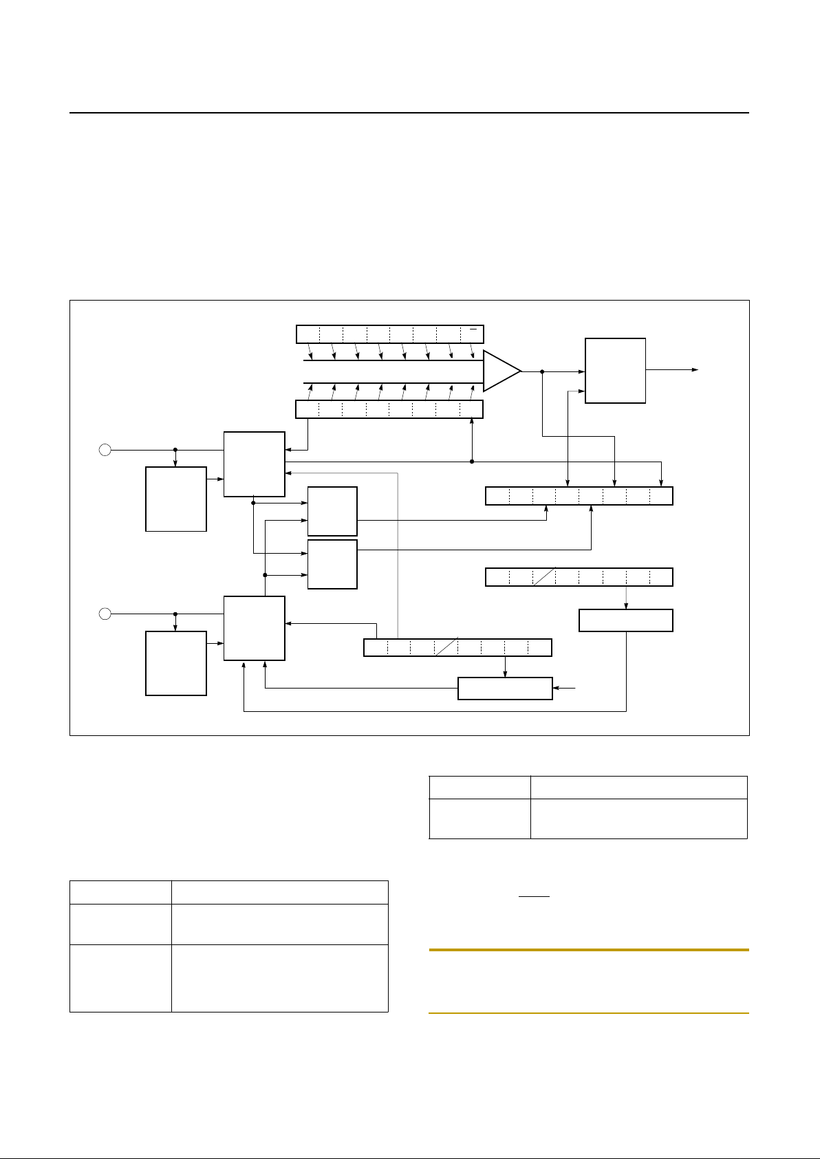
GMS81C4040/87C4060
PRELIMINARY
62
PRELIMINARY
Nov. 1999 Ver 1.0
18. I2C Bus Interface
The I2C Bus interface circuit is shown in Figure 18-1 .
The multi-mas t er I
2
C Bus interface is a serial communica-
tions circuit, conforming to the Phlips I
2
C Bus data transfer format. This interface, offering both arbitration lost
detection and a synchronous fun ctions, is useful for the
mult i- master s er i al co m mu n icatio ns.
This multi-master I
2
C Bus interface circuit consists of the
I
2
C address register, the I2C data shift register , the I2C
clock control register, the I
2
C control register, the I2C sta-
tus register and other control circuits.
The more details about registers are shown Figure 18-2 ~
Figure 18-6 .
Figure 18-1 Block Diagram of mult i-master I2C circuit
Control
The GMS81C4040/G MS87C4060 contains two I
2
C Bus
interface modules. It supports multi-master function, so it
contains arbitration lost detection, synchronization function, etc.
I
2
C address register
It contains slave address (7bit) which is used during slave
mode and Read/Write
bit.
Bit 7 ~ 0 : Slave address 6~0
Note:
Bit 7~0 (SAD6~0) store slave address. The address
data transmitted fro m the master is compared wit h the contents of these bits.
ICAR [D8H]
IFI2CR
Bit counter
SCL
Address
comparator
ICDR [D9H]
D7 D6 D5 D4 D3 D2 D1 D0
Interrupt
Generation
Circuit
Data
Control
Circuit
ICSR [00DA
H
]
MST TRX BB PIN AL AAS AD0 LRB
Noise
Elimination
Circuit
AL
Circuit
BB
Circuit
Clock
Control
Circuit
Noise
Elimination
Circuit
ICCR1 [00DB
H
]
BSEL1~0
ALS ESO
BC2~0
ICCR2 [DCH]
ACLK ACK 1
CCR3~0
Clock division
External clock
SDA
SAD6 SDA5 SDA4 SDA3 SDA2 SDA1 SDA0 R/W
ITEM Function
Format
Philips
I2C standard
7bit addressing format
Communication
mode
Master transmitter
Master recei ver
Slave transmitter
Slave receiver
SCL clock
frequency
66.6KHz ~ 500KHz (f
ex
=12MHz)
44.4KHz ~ 333.3KHz (f
ex
=8MHz)
ITEM Function
Page 67
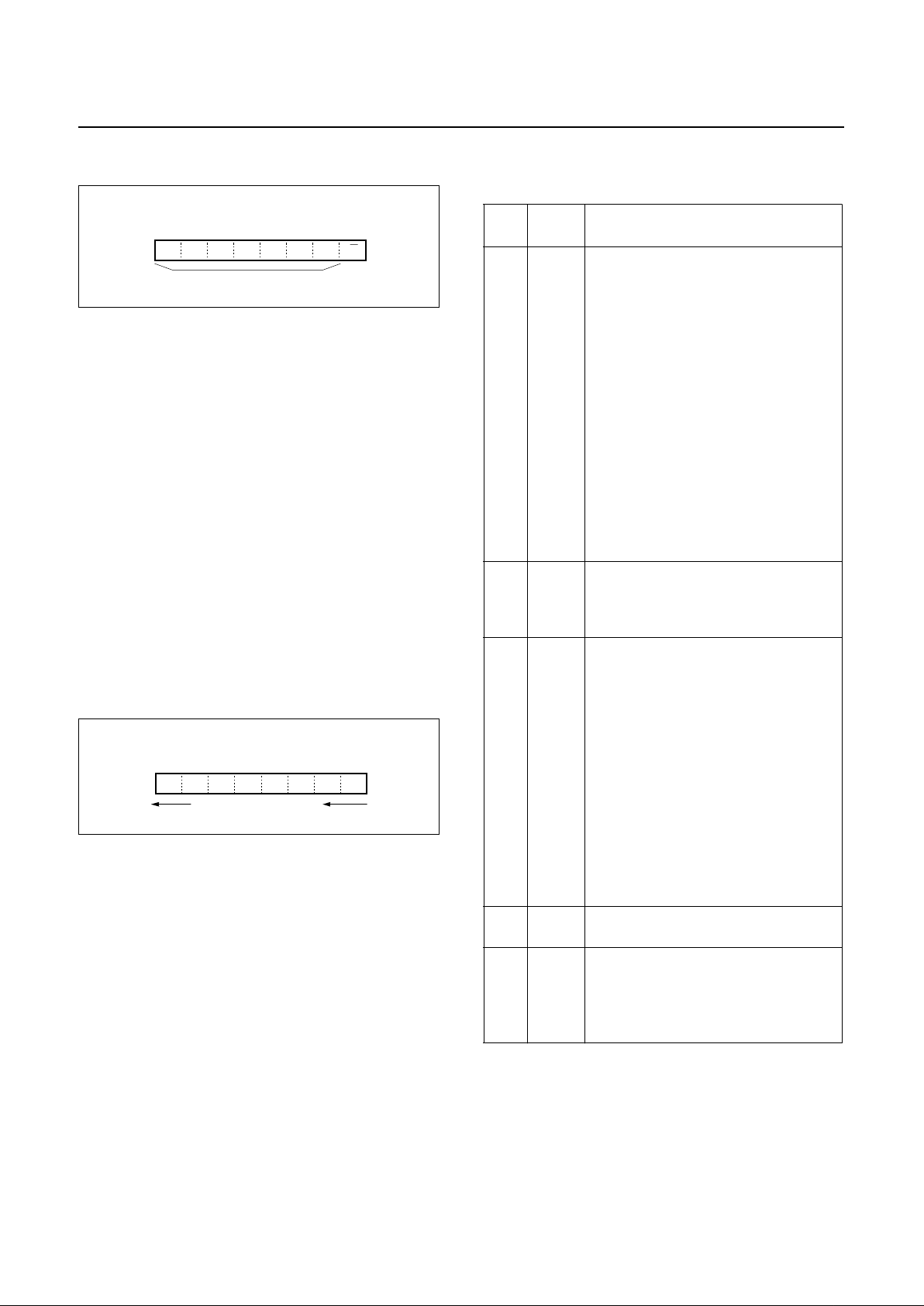
PRELIMINARY
GMS81C4040/87C4060
Nov. 1999 Ver 1.0
PRELIMINARY
63
Figure 18-2 I2C address Register
I2C data shift register [ICDR]
The I
2
C data sh ift r e gist er i s a n 8b it s hif t re gis ter to sto re
received data and write transmit data.
When transmit data is written into this register, it is trans-
fered to the outside from bit7 in synchronization with the
SCL clock, and each time one-b it data is outp ut, the data of
this register are shifted one bi t to the left. Wh en data is received, it is input to this register from bit0 in sync hronization with the SCL clock, and each time one-bit data is
input, the data of this register ar e shifted one bit to the left.
The I
2
C data shift register is in a write enable status only
when the ESO bit of the I
2
C control register (address
00DC
H
) is “1”. The bit counter is reset by a write instruc-
tion to the I
2
C data shift register. Reading data from the
I
2
C data shift register is always enabled regardless of the
ESO bit value.
Figure 18-3 Data shift register
I2C status register
The I
2
C status register controls the I2C Bus interface status. The low-order 4bits are read only bits and the high -order 4bits can be read out and writt en to.
The more details about its bits are shown Table 18-1.
ICAR
ADDRESS : 00D8
H
RESET VALUE : 0000 0000
b
SAD6
SDA5 SDA4 SDA3 SDA2 SDA1 SDA0 R/W
Slave address
RW RW RW RW RW RW RW R
ICDR
ADDRESS : 00D9
H
RESET VALUE : 0000 0000
b
RW RW RW RW RW
RW RW
RW
D7 D6 D5 D4 D3 D2 D1 D0
Sh ift left 1 - b it e a ch SC L
Bit
No.
Name Function
7
6
MST
TRX
00: Slave / Receiver mode
01: Slave / Transmitter mo de
10: Master / Receiver mode
11: Master / Transmitter mode
MST is cleared when
- After reset.
- After the arbitrat ion lost is occured and
1 byte data transmission is finished.
- After stop condition is detected.
- When start condition i s disabled by
start condition duplication preventation
function.
TRX is cleared when
- After reset.
- When arbitration lost or stop condition
is occured .
- When MST is ‘0’, and start condi ti on
or ACK non-return mode is detected.
5BB
BB(Bus busy)bit is 1 during bus is busy.
This bit can be wri tten b y S/W. it s valu e
is ‘1’ by start condition, and cleared by
stop condition.
4PIN
PIN(Pending Interr upt Not )bit is interrupt request bit.
If I
2
C interrupt request is issued, its
value is 0.
PIN is cleared when
- After 1 byte trasmission / receive is finished.
PIN is set when
- After reset.
- After write instruction is excuted into
I
2
C data shift register ICDR.
- When PIN bit low, the output of SCL is
pulled down, So if you want to release
SCL, you must perfor m writ e instr ucti on
CDR.
3AL
Arbitration los t detection flag.
If arbitration lost is detected, AL=1, or 0.
2 AAS
Slave address compari son flag.
It shows compared result with received
address data and I
2
C address register
(ICAR).
It is 1, when two of data is same.
Table 18-1 Bit functi on
Page 68
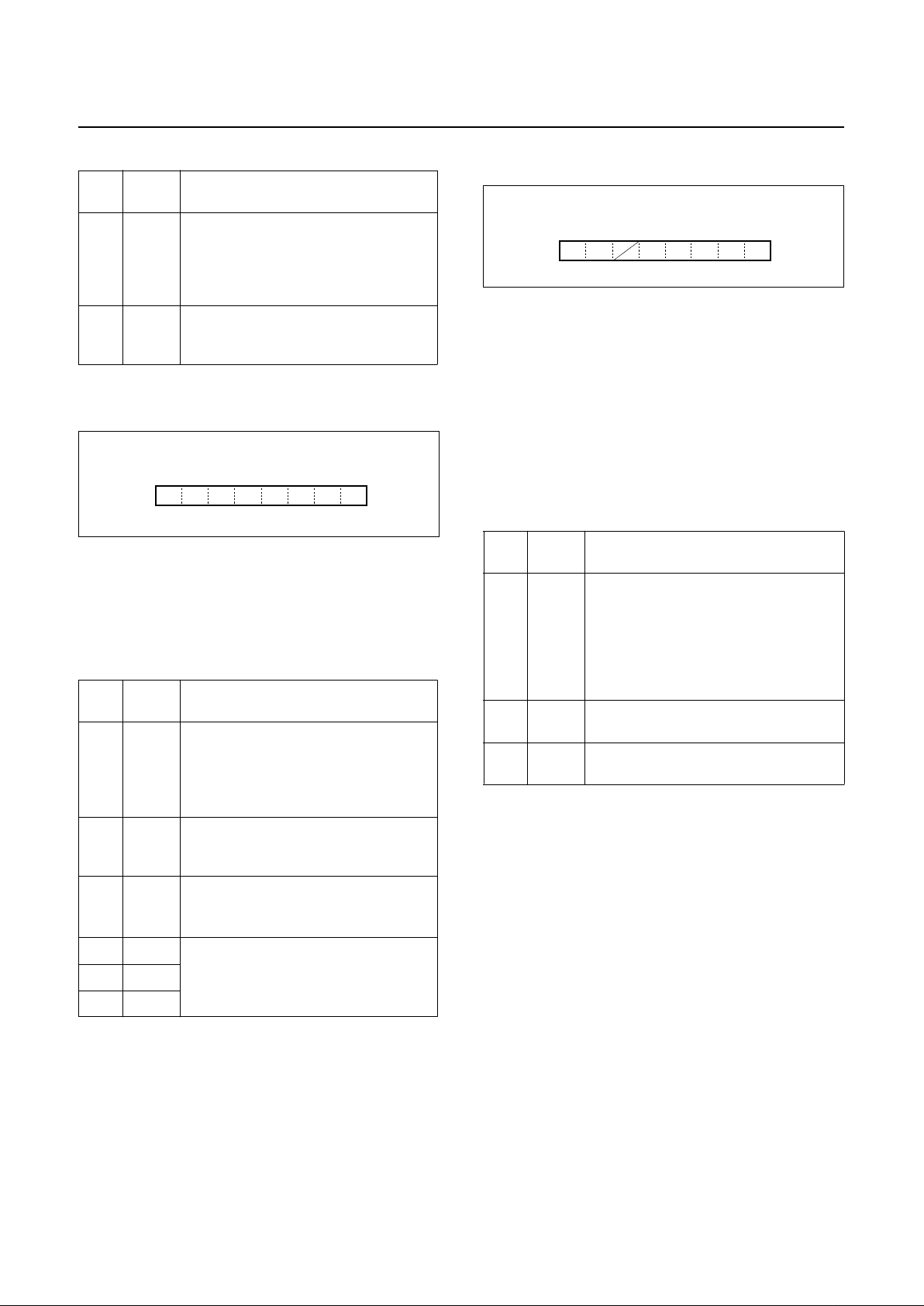
GMS81C4040/87C4060
PRELIMINARY
64
PRELIMINARY
Nov. 1999 Ver 1.0
Figure 18-4 I2C status Register
I2C control register 1
It controls communication data format.
Figure 18-5 I2C control Register 1
I2C control register 2
It controls SCL mode, SCL frequency, etc.
It contains 8bit data to transmit to external device when tr -
asmitt er m o de, or re ceiv ed 8bi t d ata f rom ex ter nal devi ce
when receive mod e .
1AD0
General call detection flag.
If general call is detected, AD0=1, or
not 0.
* General call : If recei ved add ress is all
‘0’ . it is called general call.
0LRB
Last received bit.
it is used for receive confirmation. If
ACK is returned, LRB=0, or not 1.
Bit
No.
Name Function
76BSEL1
BSEL0
I
2
C connection cont rol.
00: No connection
01: SCL1, SDA1
10: SCL2, SDA2
11: SCL1, SDA1, SCL2, SDA2
4ALS
Data format sele cti on.
0: Addressing f ormat
1: Free data format
3 ESO
I
2
C Bus interface use ena ble flag
0: Disabled
1: Enabled
2BC2
Bit counter.
000
b
: 8bit
001
b
~111b: 1~7bit
1BC1
0BC0
Table 18-2 Bit function
Bit
No.
Name Function
Table 18-1 Bit function
ICSR
ADDRESS : 00DA
H
RESET VALUE : 0001 0000
b
RW
RW RW RW R
RRR
MST TRX BB PIN AL AAS AD0 LRB
Bit
No.
Name Function
7ACLK
Select acknowledge clock (ACK) mode.
0: No acknowledge clock mode.
acknowledge clock is not generated
after data was transmismitted.
1: acknowledge clock mode .
acknowledge clock is generated after
data was transmismitted.
6ACK
If acknowledge cl ock is r eturne d, t his bi t
is 0. Or not 1.
5
1
(fixed)
Not used.
Table 18-3 Bit function
ICCR1
ADDRESS : 00DB
H
RESET VALUE : 00-0 0000
b
ALS ESO BC2 BC1 BC0
BSELBSEL
10
RW RW
RW
RW RW RW RW
Page 69
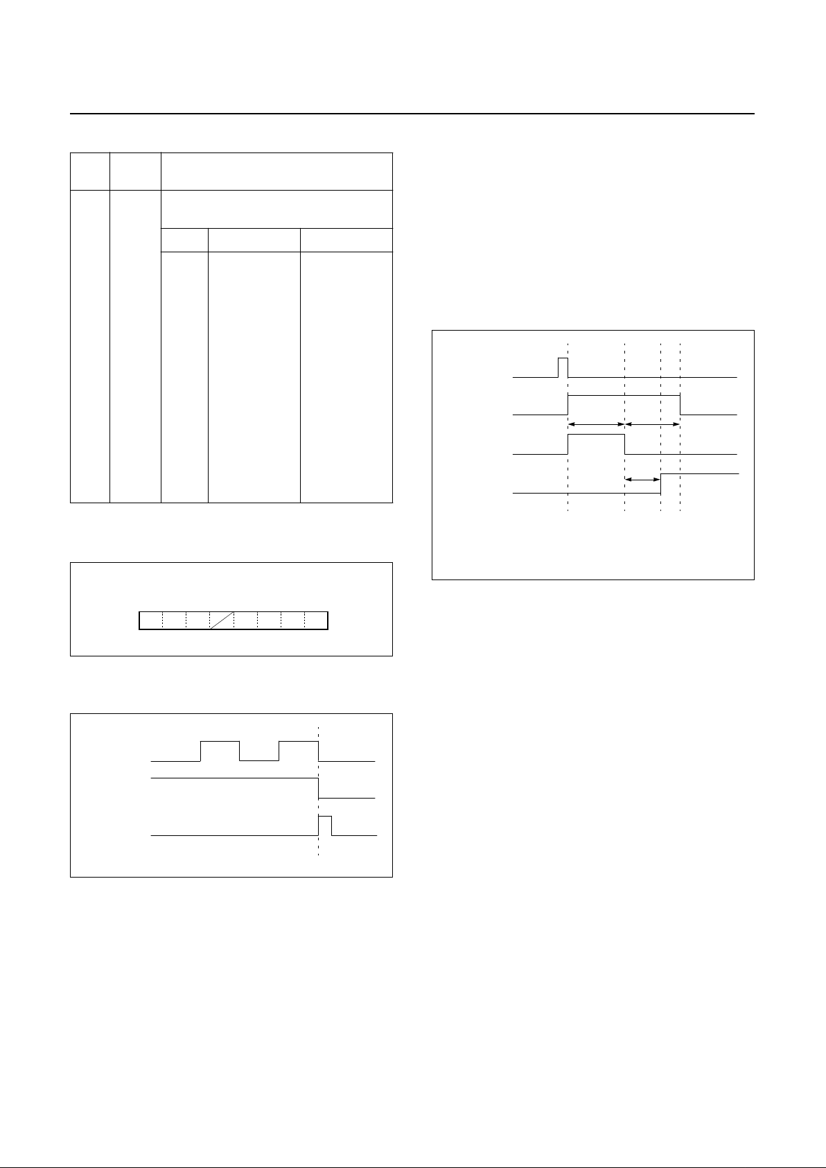
PRELIMINARY
GMS81C4040/87C4060
Nov. 1999 Ver 1.0
PRELIMINARY
65
Figure 18-6 I2C control Register 2
Figure 18-7 Interrupt request signal generation timing
START conditi on gene ra tion
When the ESO bit of the I
2
C control register (00DBH) is
“1”, wr it ing t o t he I
2
C status regist er wi ll gene rate ST ART
condition. Refer to Figure 18-8 for the START condition
generation ti mi ng diagram.
Figure 18-8 START condition generation timing
RESTART condi t i on gene ration
RESTART conditi on’s setting sequen ce is as followings.
1. Write 020
H
to I2C status register (ICSR, 00DAH)
2. Write slave a ddress to I
2
C data shift register (ICD R,
00D9
H
)
3. Write 0F0
H
to I2C status register (ICSR, 00DAH)
STOP condition gen erati on
Writing ‘C0 h’ to ICSR will genera te a s top c onditio n,
3
2
1
0
CCR3
CCR2
CCR1
CCR0
SCL Frequency selection
SCL frequency = f
ex
/ (12 * CCR)
Value
f
ex
= 12MHz fex = 8MHz
0000
0001
0010
0011
0100
0101
0110
0111
1000
1001
1010
1011
1100
1101
1110
1111
Not allowed
Not allowed
500.0KHz
333.3KHz
250.0KHz
200.0KHz
166.6KHz
142.9KHz
125.0KHz
111.1KHz
100.0KHz
90.0KHz
83.3KHz
76.4KHz
71.4KHz
66.6KHz
Not allowed
Not allowed
333.3KHz
222.2KHz
166.6KHz
133.3KHz
111.1KHz
95.2KHz
83.3KHz
74.1KHz
66.6KHz
60.6KHz
55.5KHz
51.3KHz
47.6KHz
44.4KHz
Bit
No.
Name Function
Table 18-3 Bit function
ICCR2
ADDRESS : 00DC
H
RESET VALUE : 000- 0000
b
RW RW RW RW RW RW
ACLK
ACK 1
CCR3
CCR2
CCR1 CCR0
SCL
PIN
I
2
C Request
ICSR write signal
SCL
SDA
BB (Bus busy) flag
t
SETUP
t
HOLD
t
BB
: Setup time
: Hold time
: Set time for BB
t
SETUP
t
HOLD
t
BB
(I2C status reg.)
Page 70
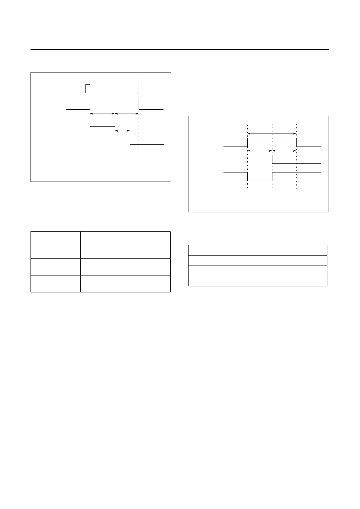
GMS81C4040/87C4060
PRELIMINARY
66
PRELIMINARY
Nov. 1999 Ver 1.0
w h e n E S O ( I C C R b i t 3 ) is ‘ 1 ’
Figure 18-9 STOP condi tion generating t iming diagram
START / STOP condition generation time is shown Table
18-4.
START / STOP condition detect
START / STOP condition is detected when Table 18-4 is
satisfied.
Figure 18-10 START / STOP condition detection timing
START / STOP detection time is showed Table 18-5.
ITEM Timing SPEC.
Setup time
( t
SETUP
)
3.3uS (n=20cycles )
Hold time
( t
HOLD
)
3.3uS (n=20cycles )
Set/Reset time for
BB flag ( t
BB
)
3.0uS (n=18cycles )
Table 18-4 Example time ( f
ex
=12MHz )
ICSR write signal
SCL
SDA
BB (Bus busy) flag
t
SETUPtHOLD
t
BB
: Setup time
: Hold time
: Set time for BB
t
SETUP
t
HOLD
t
BB
(I2C status reg.)
ITEM Timing SPEC.
SCL release time > 2.0uS (n=12cycles)
Setup time > 1.0uS (n=6cycles)
Hold time > 1.0uS (n=6cycles)
Table 18-5 Example time ( f
ex
=12MHz )
SCL
SDA (START)
SDA (STOP)
t
SETUPtHOLD
: Setup time
: Hold time
t
SETUP
t
HOLD
SCL release time
Page 71
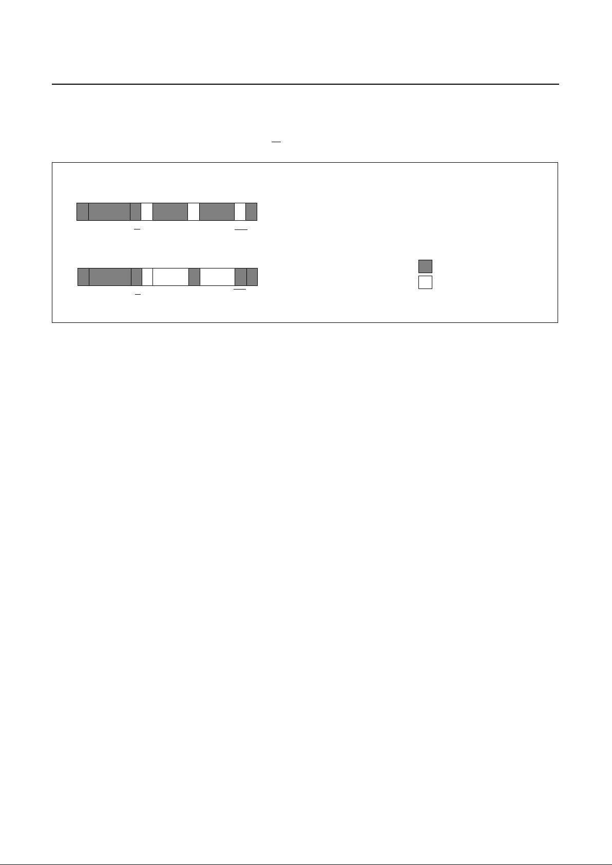
PRELIMINARY
GMS81C4040/87C4060
Nov. 1999 Ver 1.0
PRELIMINARY
67
Address data communication
The first transmitted data from master is compared with
I
2
C address registe r (ICA R, 00D 8H). At this time R/W is
not compared but it determines next data ope ration. i.e,
transmitting or receiving data
Figure 18-11 Address data comm unication format
Master -> Slave (with 7bit address)
START
R/W
ACK
ACK
ACK
/ACK
Data
STOP
Slave addr.
Slave -> Master (with 7bit address)
Data block from master to slave
Data block from slave to master
7bit
Data
START
R/W
ACK
ACK
ACK
Data
STOP
Slave addr.
7bit
Data
(“1”)
(“0”)
Page 72
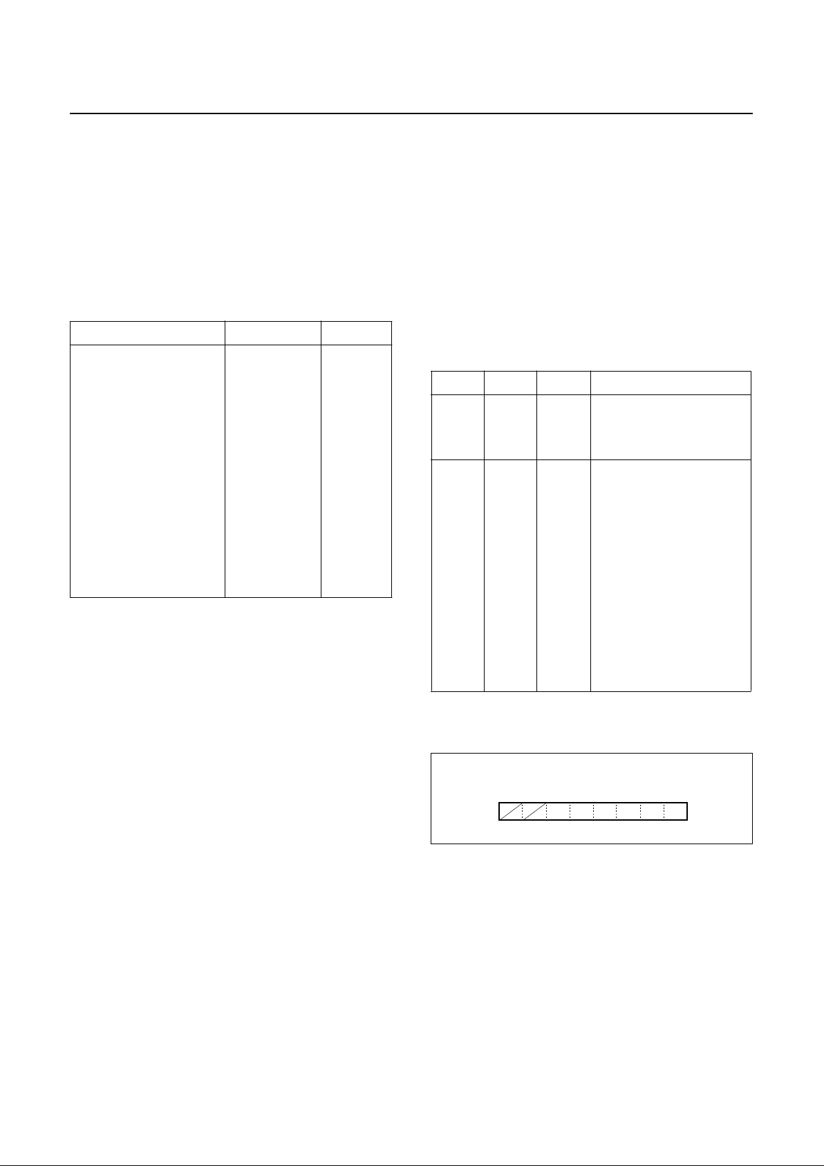
GMS81C4040/87C4060
PRELIMINARY
68
PRELIMINARY
Nov. 1999 Ver 1.0
19. INTERRUPTS
The GMS81C4040/G MS87C4060 interrupt c ircuits consist of Interrupt enable register (IENH, IENL) , Interrupt request flags of IRQH , IRQL, Priority circuit and Master
enable flag ("I" flag of PSW). 16 interr upt sourc es are provided. The configuration of interrupt circuit is shown in
Figure 19-2 .
Below table shows the Interrupt priority
The External I nterrupt s c an each be t ransi tion-a ctiva ted (1to-0 or 0-to-1 transition ).
When an external interrupt is generated, the flag that generated it is cleared by the hardware when the service routine is vect ored to o nly if the int errupt was tr ansitio nactivated.
The Timer/Counter Interrupts are generated by
TnIF(n=0~3), which is set by a match in their respective
timer/counter register.
The Basic Interval Timer Interrupt is generated by BITIF
which are set by a over f low in the timer regi ster.
The inte rr upt s ar e cont rol l ed b y th e i nte rrup t ma st er ena bl e
flag I-flag (bit 2 of PSW), the interrupt enable register
(IENH, IENL) and the interrupt request flags (in
IRQH,IRQL) except Power-on reset and software BRK interrupt.
Interrupt Mode Register
It controls interr upt priority . I t takes only one specified interrupt.
Of course, interrupt’s priority is fixed by H/W, but sometimes user want to get specified interrupt even if higher
prior ity int err upt was occ u red . Hi ghe r pr iori ty int err up t is
processed the next time.
It contains 2bit data to enable priority selection and 4bit
data to select specified interrupt.
Figure 19-1 Interrupt Mode Register
Reset/Interrupt Symbol Priority
Hardware Reset
Extern a l In te r ru p t 0
OSD Inte r ru pt
Extern a l In te r ru p t 1
Extern a l In te r ru p t 2
Timer/Counter 0
Timer/Counter 2
1 Frame Interrupt
VSync Interrupt
Timer/Counter 1
Timer/Counter 3
Interrupt interval measure
Watchdog Timer
Basic Interval Timer
Serial I/O Interrupt
I
2
C Interr u p t
RESET
INT0
OSD
INT1
INT2
Timer 0
Timer 2
1Frame
VSync
Timer 1
Timer 3
INTV(INT3/4)
WDT
BIT
SIO
I2C
1
2
3
4
5
6
7
8
9
10
11
12
13
14
15
Bit No. Name Value Function
5,4 IM1~0
00
01
1X
Mode 0: H/W priority
Mode 1: S/W priority
Interrupt is disabled, even
if IE is set.
3~0 IP3~0
0000
0001
0010
0011
0100
0101
0110
0111
1000
1001
1010
1011
1100
1101
1110
1111
INT0
OSD
INT1
INT2
Timer 0
Timer 2
1Frame
VSync
Timer 1
Timer 3
INTV(INT3/4)
WDT
BIT
SIO
I2C
Not used
Table 19-1 Bit functi on
IMOD
ADDRESS : 00F3
H
RESET VALUE : Undefined
IM0 IP3 IP2
IP1
IP0
RW RW RW RW RW RW
IM1
Page 73
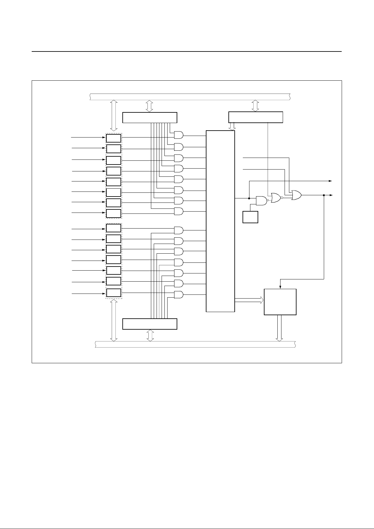
PRELIMINARY
GMS81C4040/87C4060
Nov. 1999 Ver 1.0
PRELIMINARY
69
Figure 19-2 Block Diagram of Interrupt
T0
Timer 0
INT2
INT1
INT2
INT1
IFOSD
OSD
INT0
INT0
IENH [00F6H]
Interrupt Enable
IRQH
Interrupt
Vector
Address
Generator
Internal bus line
Register (Higher byte)
To CPU
Interrupt Master
Enable Flag
I Flag
Priority Control
I-flag i s in PS W, it i s c leare d by "DI", s e t by
"EI" instruction. When it goes interrupt service,
I-flag is cleared by hardw are, thus any other
interrupt are inhibited. When interrupt service is
comp le ted b y "RET I" in s truct ion, I- fla g is s et to
"1" by hardware.
T2
Timer 2
1Frame
1 Frame
VSync
IFVSync
WDT
IFWDT
IFBIT
IFS
BIT
SR
IFI2C
I2C
IENL [00F4H]
IRQL
INTV
Intr. interva l
T3
Timer 3
T1
Timer 1
[00F5H]
Internal bus line
IMOD [00F3H]
Bit5
Interrupt Enable
Register (Lower byte)
RESET
BRK
[0F7
H
]
Page 74
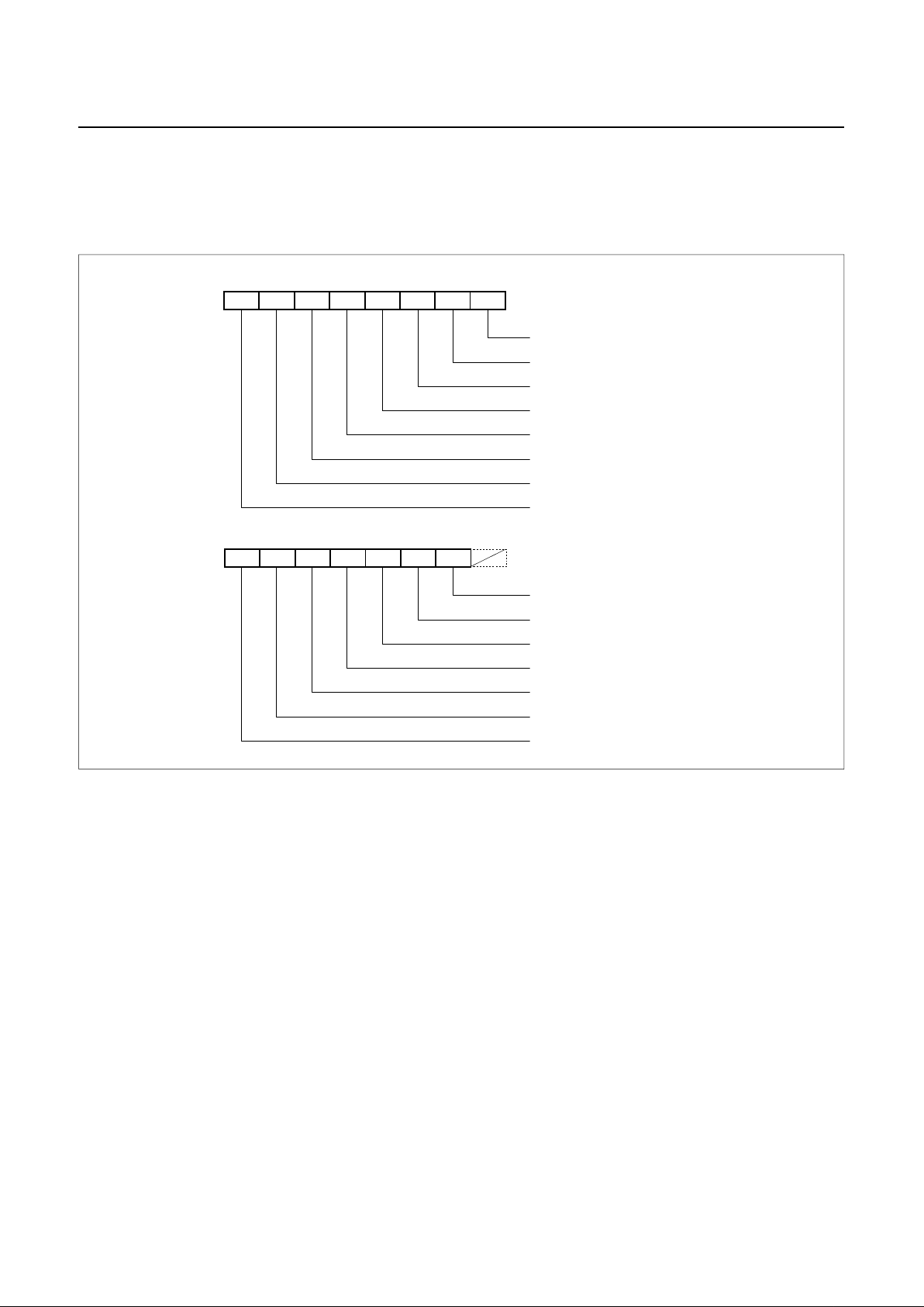
GMS81C4040/87C4060
PRELIMINARY
70
PRELIMINARY
Nov. 1999 Ver 1.0
Interrupt enable registers are shown in Figure 19-4 . These
registers are composed of interrupt enable flags of each interrupt source, these flags determines whether a n interrupt
will be accept ed or not. W hen enab le flag is "0", a co rre-
sponding interrupt sour ce is prohibited. No te that PSW
contains also a master enable bit, I-flag, which disables all
interrupts at once.
Figure 19-3 Inte rrupt Request Flags
INT2
R/W
INT0
VSync interrupt request flag
INITIAL VALUE: 0000 0000
b
ADDRESS: 00F7
H
IRQH
OSD
MSB LSB
1Frame
VSync
T0
T2INT1
R/W R/W
WDT
R/W
T1
INITIAL VALUE: 0000 000-
b
ADDRESS: 00F5
H
IRQL
T3
MSB
I2CBIT
INTV
R/W
R/W R/W
SR
R/W R/W R/W
R/W R/W R/W R/W R/W
1 Frame interrupt request flag
Timer / Counter 2 interrupt request flag
Timer / Counter 0 interrupt request flag
External interrupt 2 interrupt request flag
External interrupt 1 interrupt request flag
On screen display interrupt request flag
External interrupt 0 interrupt request flag
I
2
C interrupt request flag
LSB
Serial I/O interrupt request flag
Basic interval timer interrupt request flag
Watch-dog timer interrupt request flag
Interrupt interval measurement interrupt request flag (INT3/4)
Timer / Counter 3 interrupt request flag
Timer / Counter 1 interrupt request flag
Page 75
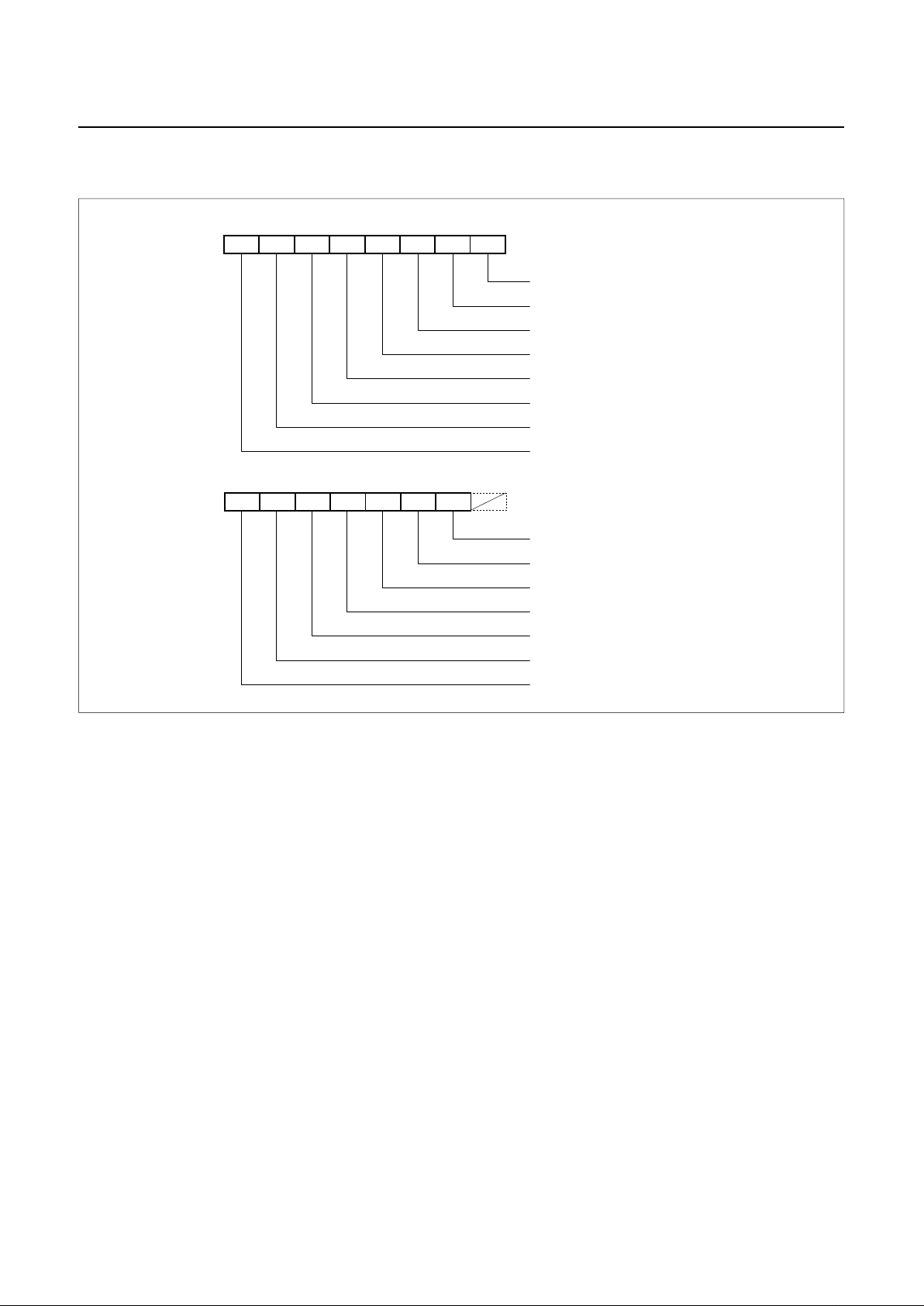
PRELIMINARY
GMS81C4040/87C4060
Nov. 1999 Ver 1.0
PRELIMINARY
71
Figure 19-4 Interrupt Enable Flags
INT2
R/W
INT0
VSync interrupt enable flag
INITIAL VALUE: 0000 0000
b
ADDRESS: 00F6
H
IENH
OSD
MSB LSB
1Frame
VSync
T0
T2INT1
R/W R/W
WDT
R/W
T1
INITIAL VALUE: 0000 000-
b
ADDRESS: 00F4
H
IENL
T3
MSB
I2CBIT
INTV
R/W
R/W R/W
SR
R/W R/W R/W
R/W R/W R/W R/W R/W
1Frame interrupt enable flag
Timer / Counter 2 interrupt enable flag
Timer / Counter 0 interrupt enable flag
External interrupt 2 interrupt enable flag
External interrupt 1 interrupt enable flag
On screen display interrupt enable flag
External interrupt 0 interrupt enable flag
I
2
C interrupt enable flag
LSB
Serial I/O interrupt enable flag
Basic interval timer interrupt enable flag
Watch-dog timer interrupt enable flag
Interrupt interval measurement interrupt enable flag (INT3/4)
Timer / Counter 3 interrupt enable flag
Timer / Counter 1 interrupt enable flag
Page 76
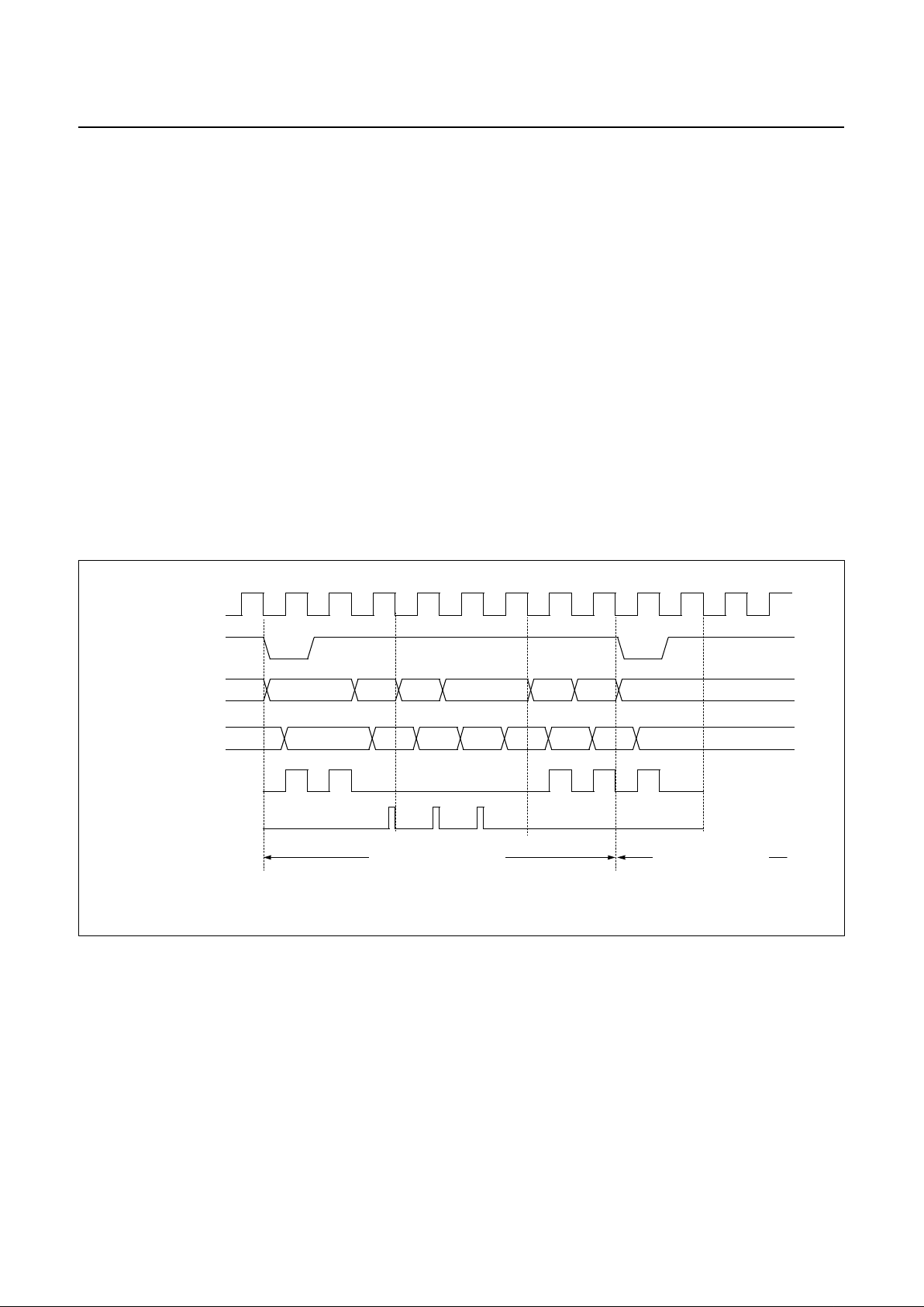
GMS81C4040/87C4060
PRELIMINARY
72
PRELIMINARY
Nov. 1999 Ver 1.0
19.1 Interrupt Sequence
An inte rru pt requ est is held u ntil th e inter rupt is acce pted
or the interrupt latch is cleared to "0" by a reset or an instruction. Interrupt acceptance sequence requires 8 f
ex
(2
µs at f
MAIN
=4MHz) after the c ompletion of the curren t instruction execution. The interrupt service task terminates
upon execution of an interrupt return instruction [RETI].
Interrupt acceptance
Figure 19-5 Inte rrupt Service routine Ente ring Timing
1. The interrupt master enable flag (I-flag) is cleared to
"0" to temporarily disable the acceptance of any following maskable interrupts. When a non-maskable interrupt is accepted, the acceptance of any following
inter r u pt s is tempo r ar ily dis a bled.
2. Interrupt request flag for the int errupt source accepted
is clear ed to "0".
3. The contents of the program counter (return address)
and the program status word are saved (pushed) onto
the stack area. The stack pointer decrements 3 times.
4. The entry address of the interrupt service program is
read from the vector table address, and the entry address is loaded to the pro gram counter.
5. The instruction stored at the entry address of the interrupt service program is executed.
V.L.
System clock
Address Bus
PC
SP SP-1
SP-2 V.H. New PC
V.L.
Data Bus
Not used
PCH PCL
PSW ADL OP codeADH
Instruction Fetch
Internal Read
Internal Write
Interrupt Processing Step Interrupt Service Task
V.L. and V.H. are vector addresses.
ADL and ADH are start addresses of interrupt service routine as vector contents.
Page 77
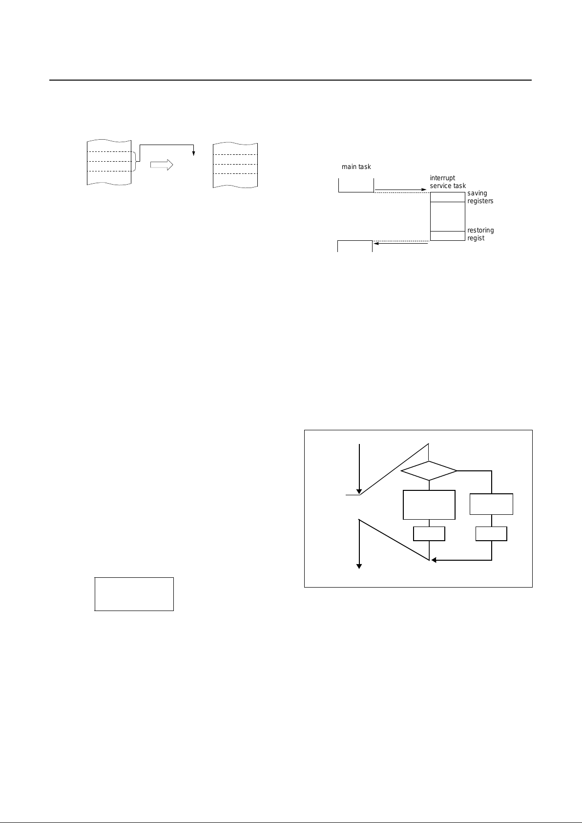
PRELIMINARY
GMS81C4040/87C4060
Nov. 1999 Ver 1.0
PRELIMINARY
73
A maskable interrupt is not accepted until the I-flag is set
to "1" even if a maskable interrupt of higher priority than
that of the curre nt interrupt being serviced.
When nested interrupt se rvice is nece ssary, the I-flag is set
to "1" in the in ter rupt servi ce prog ram. In t his c ase , a ccep table interrupt sources are selectively enabled by the individual interrupt enable flags.
Saving/Restoring General-purpose Register
During inter rupt acceptance process ing, the program
counter and the program status word are automatically
saved on the stack, but not the accumulator and other registers. These registers are saved by the program if necessary. Also, when nesting multiple interrupt services, it is
necessary to avoid using the same data memory area for
saving registers.
The following method is used to save/restore the generalpurpose registers.
Example: Register save using push and pop instructions
General-purpose register save/restore using push and pop
instructions;
19.2 BRK Interrupt
Software interrupt can be invoked by BRK instruction,
which is the lowest priority order.
Interrupt vector address of BRK is shared with the vector
of TCALL 0 (Refer to Program Memory Section). When
BRK interrupt is generated, B-flag of PSW is set to distinguish BRK from TCALL 0.
Each processing step is determined by B-flag as shown in
Figure 19-6 .
Figure 19-6 Execution of BRK/TCALL0
INTxx: PUSH A
PUSH X
LDA DPGR
PUSH A
;SAVE ACC.
;SAVE X REG.
;SAVE DPGR
; Direct page
; accessable reg.
;
:
interrupt processing
:
POP A
STA DPGR
POP X
POP A
RETI
;RESTORE DPGR
;RESTORE X REG.
;RESTORE ACC.
;RETURN
Basic Interval Timer
012
H
0E3
H
0FFE6
H
0FFE7
H
0E
H
2E
H
0E312
H
0E313
H
Entry Address
Correspondence between vector table address for BIT interrupt
and the entry address of the interrupt service program.
Vector Table Address
main task
interrupt
service task
saving
registers
restoring
registers
acceptance of
inter ru p t
interrupt return
B-FLAG
BRK
INTERRUPT
ROUTINE
RETI
TCALL0
ROUTINE
RET
BRK or
TCALL0
=0
=1
Page 78
GMS81C4040/87C4060
PRELIMINARY
74
PRELIMINARY
Nov. 1999 Ver 1.0
19.3 Multi Interrupt
If two requests of different priority levels are received simultaneously, the request of higher priority level is serviced. If requests of the same priority level are received
simultaneously, an internal polling sequence determines
by hardware which request is serviced.
Figure 19-7 Executi on of Multi Interrupt
However, multip le proc essin g t hrough s oftware for s peci al
features is possible. Gene rally when an i nterrupt is accepted, the I-flag is cle ared t o disable any furt her interrup t. But
as user set I-fl ag in inte rrupt rou tine, s ome furt her int errupt
can be serviced even if certain interrupt is in prog ress.
Example: Even though Timer1 interrupt is in progress,
INT0 interrupt serviced without any suspend.
TIMER1: PUSH A
PUSH X
PUSH Y
LDM IENH,#80H ;Enable INT0 only
LDM IENL,#0 ;Disable other
EI ;Enable Interrupt
:
:
:
:
:
:
LDM IENH,#FFH ;Enable all interrupts
LDM IENL,#FEH
POP Y
POP X
POP A
RETI
enable INT0
TIMER 1
service
INT0
service
Main Program
service
Occur
TIMER1 interrupt
Occur
INT0
EI
disable other
enable INT0
enable other
In this example, the INT0 interrupt can be serviced without any
pending, even TIMER1 is in progress.
Because of re-setting the interrupt enable registers IENH,IENL
and master enable "EI" in the TIMER1 routine.
Page 79
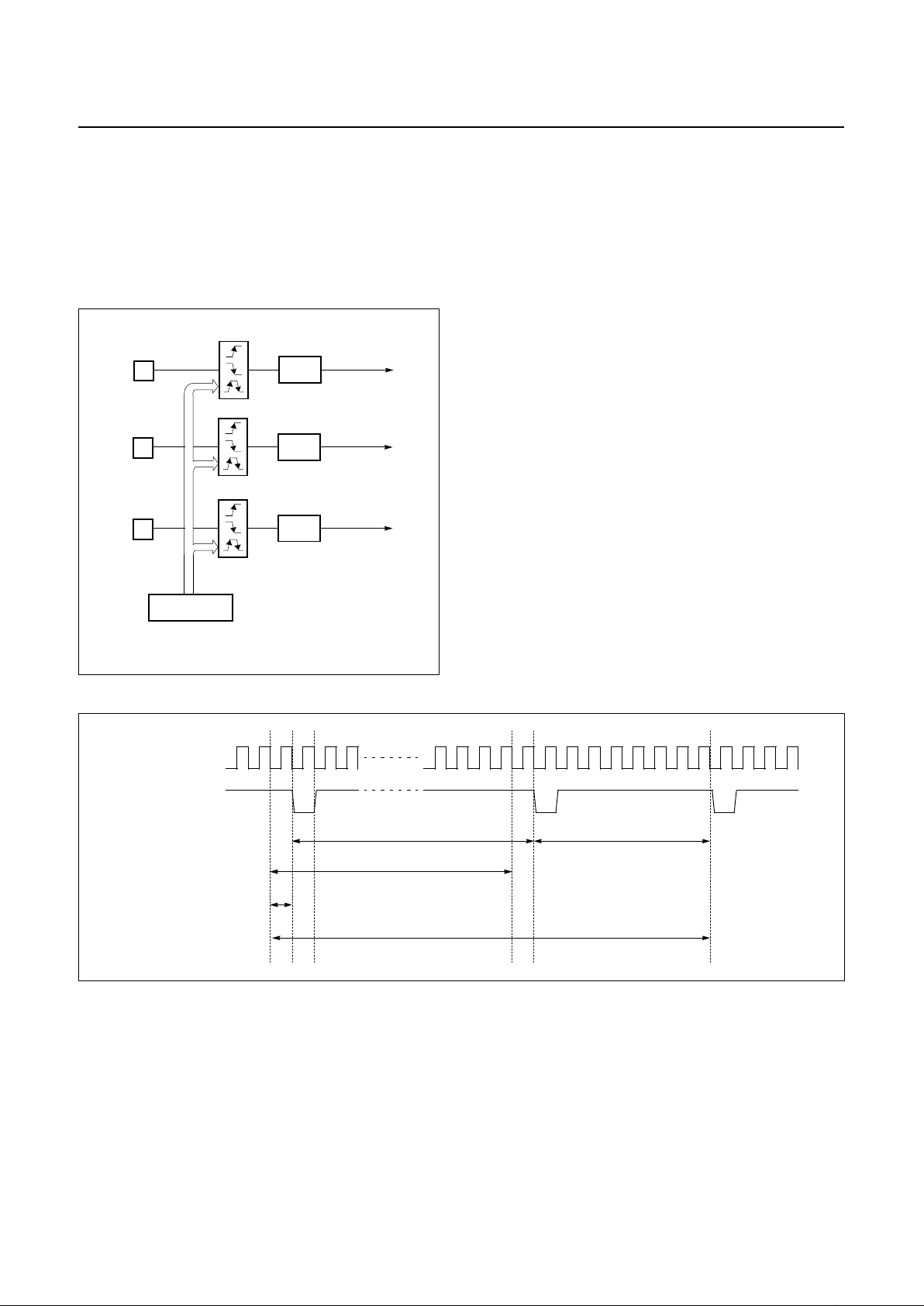
PRELIMINARY
GMS81C4040/87C4060
Nov. 1999 Ver 1.0
PRELIMINARY
75
19.4 External Interrupt
The external interrupt on INT0, INT 1.. . pins are edge triggered depending the edge selection register.
Refer to “6. PORT STRUCTURES” on page 9.
The edge dete ction of exter nal int erru pt has thre e tra nsition
activated mode: ris ing edge, falling edge, bot h edge .
Figure 19-8 External Interrupt Block Diagram
INT0, INT1 and INT2 are multiplexed with g eneral I/O
ports. To use external interr upt pin, the bit of port funct ion
register FUNC1 should be set to "1" correspondingly.
Response Time
The INT0 , IN T1 an d IN T2 ed ge ar e latch ed in to I NT0IF ,
INT1 IF and INT2IF at ever y mach ine cyc le. The values
are not actually polled by the circuitry until the next machine cycle. If a request is active and conditions are right
for it to be acknowled ged, a hardware subro utine call to t he
requested se r vice routine will be the next instruction to be
executed. For example, the DIV instruction takes twelve
machine cycles. Thus, a minimum of twelve complete machine cycles elapse between activation of an external interrupt request and the beginning of execution of the first
instruction of the service routine
Figure 19-9 Interrupt Response Timing Diagram ( Interrupt overhead )
INT0IF
INT0 pin
INT0 INTERRUPT
INT1IF
INT1 pin
INT1 INTERRUPT
INT2IF
INT2 pin
INT2 INTERRUPT
IEDS
[00F2
H
]
edge selection
System clock
Instruction Fetch
Last i nstruction execution (0~12cycle) Enter interrupt service routine (8cycle)
Interrupt request sampling
1cycle
Interrupt over haed (9~ 21cycle)
Page 80
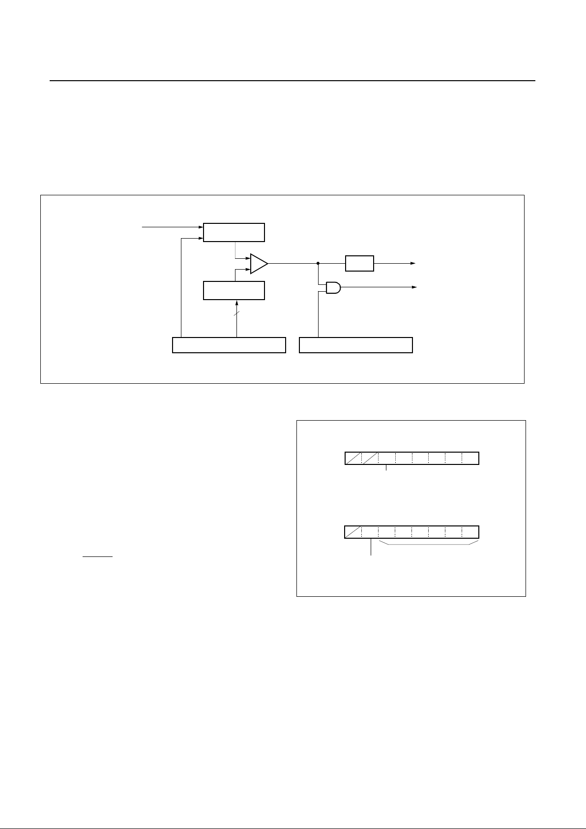
GMS81C4040/87C4060
PRELIMINARY
76
PRELIMINARY
Nov. 1999 Ver 1.0
20. WATCHDOG TIMER
The watchdog timer rapidly detects the CPU malfunction
such as endless l oopin g caused b y noise or the like, and resumes the CPU to the normal state.
The watchdog timer signal for detecting malfunction can
be selected either a reset CPU or a interrupt request.
When the watchdog timer is not being used for malfunction detection, it can be used as a timer to generate an interrupt at fixed intervals.
Figure 20-1 Block Diagram of Watchdog Timer
Watchdog Timer Control
Figure 2 0-2 shows the w atchdog ti mer control r egister.
The watchdog timer is automatically disabled after reset.
The CPU malfunction is detected as setting the detection
time, sele cting o utpu t, and c leari ng t he bina ry counte r. Repeatedly clearing the binary counter within the setting detection time.
If the malf unction occurs for any cause, the watchdog timer output will become active at the rising overflow from
the binary counters unless the binary counter are cleared.
At this time, when WDTON=1 a reset is generated, which
drives the RESET
pin low to reset the internal hardware.
When WDTON=0, a watchdog ti mer inte rrup t (I FWDT) is
generated.
Figure 20-2 Watchdog timer register
to reset CPU
WDTR
Watchdog Timer Register
(BIT overflow : IFBIT)
Clock source
6-bit up-counter
enable
WDT
6-bit compare data
comparator
6
WDTR[bit5~0]
Watchdog Timer interrupt
WDTCL[bit6]
clear
[00D7
H
]
IFWDT
CKCTLR
Clock control Register
[00D6
H
]
WDTON[bit5]
CKTCLR
ADDRESS : 00D6
H
RESET VALUE : 0000 0000
b
WDT ENP
BTCL BTS2 BTS1 BTS0
Watchdog timer On/Off control
WWWWWR
WDTR
ADDRESS : 00D7
H
RESET VALUE : -011 1111
b
WDT
WDTR5 ~ 0
Slave address
WWWWWWW
ON CK
0: Normal 6bit timer, Watchdog off
1: Watchdog timer
CL
Watchdog timer Clear
0: Watchdog timer free run
1: Watchdog timer clear and free run
Automatically cleared this bit after 1cycle
Page 81
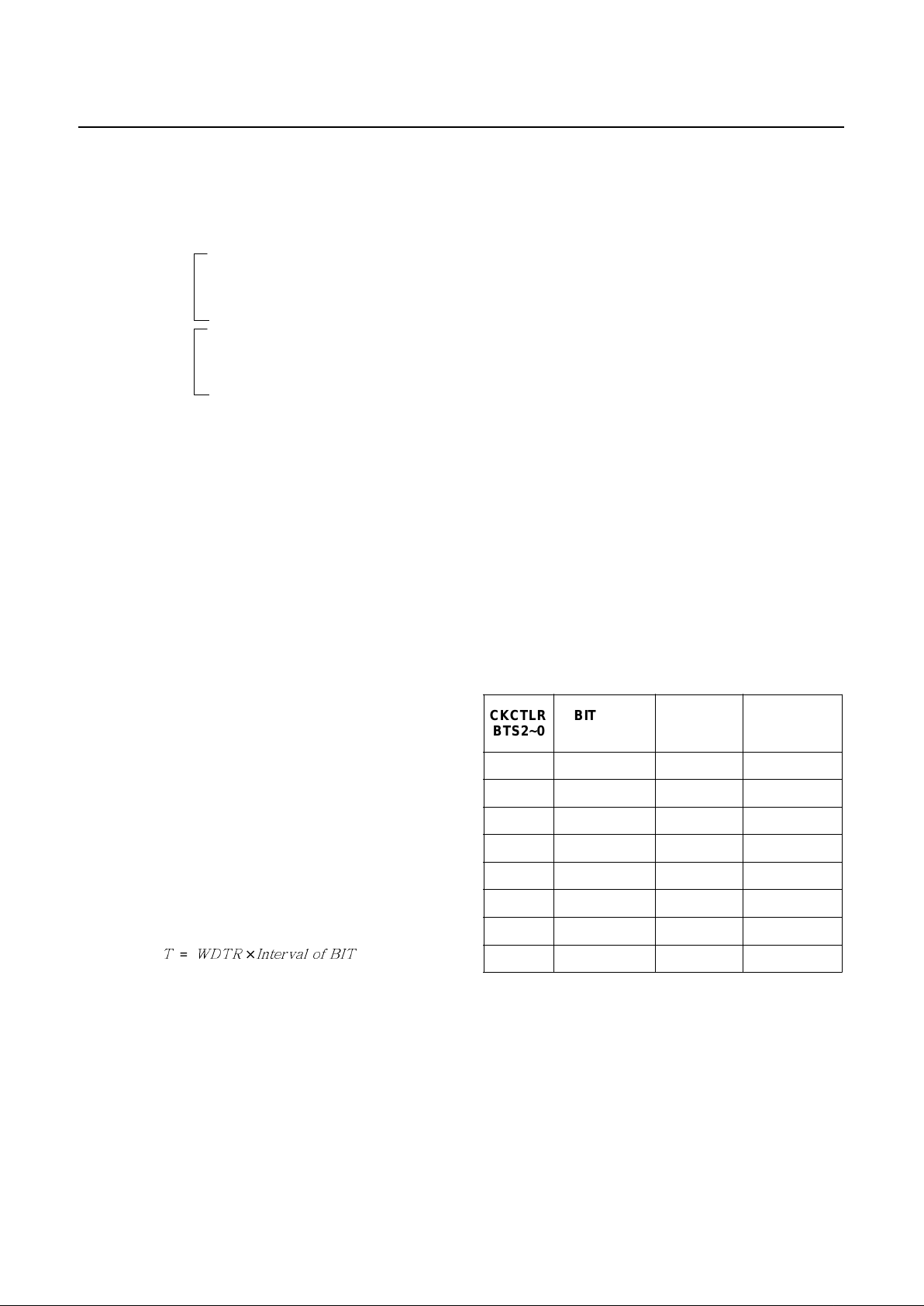
PRELIMINARY
GMS81C4040/87C4060
Nov. 1999 Ver 1.0
PRELIMINARY
77
Example: Sets the watchdog timer detecti on time
Enable and Disable Watchdog
Watchdog timer is ena bled by setting WDTO N (bit 5 in
CKTCLR) to "1". WDTON is initialized to "0" during reset, WDTON should be set to "1" to operate after reset is
released.
Example: Enables watc hdog timer reset
:
LDM CKTCLR ,# 00 1? ????b ;WD TO N←1
:
:
The watchdog timer is disab led by clearing bit 5 (WDTON) of CKTCLR.
Watchdog Timer Int errupt
The watchdog timer can also be used as a simple 6-bit timer by clearing bit 5 (WDTON) of CKTCLR. The interval
of watchdog timer interrupt is de cided by Basic Interval
Timer.
Interval equation is shown as below.
The stack pointer (SP) should be initialized before using
the watchdog timer output as an interrupt source.
Example: 6-bit timer interrupt setting up.
LDX #03FH
TXSP ;SP ← 3F
LDM CKTCLR,#000?????b ;WDTON←0
LDM WDTR,#01??????b ;WDTCL←0
:
:
Refer table and see BIT timer ().
LDM WDTR,#01??????b ;Clear Counter and set value(??????b)
;You have to set WDTR first, for prevent unpredictable interrupt
;when you set WDTON bit.
LDM CKCTLR,#00111???b ;Sele ct clock source(???b) and WDTON=1
LDM WDTR,#01??????b ;Clear counter
:
:
:
:
LDM WDTR,#01??????b ;Clear counter
:
:
:
:
LDM WDTR,#01??????b ;Clear counter
Within WDT
detection tim e
Within WDT
detection time
×=
CKCTLR
BTS2~0
BIT input
clock
Watchdog
timer input
clock
IFWDT cycle
000
b
PS4 (2uS) 512uS 32,256uS
001
b
PS5 (4uS) 1,024uS 64,512uS
010
b
PS6 (8uS) 2,048uS 129,024uS
011
b
PS7 (16uS) 4,096uS 258,048u S
100
b
PS8 (32uS) 8,192uS 516,096u S
101
b
PS9 (64uS) 16,384uS 1,032,192uS
110
b
PS10 (128uS) 32,7 68uS 2,06 4,384uS
111
b
PS11 (256uS) 65,5 36uS 4,12 8,768uS
Table 20-1 Watchdog timer MAX. cycle (Ex:f
ex
=8MHz)
Page 82
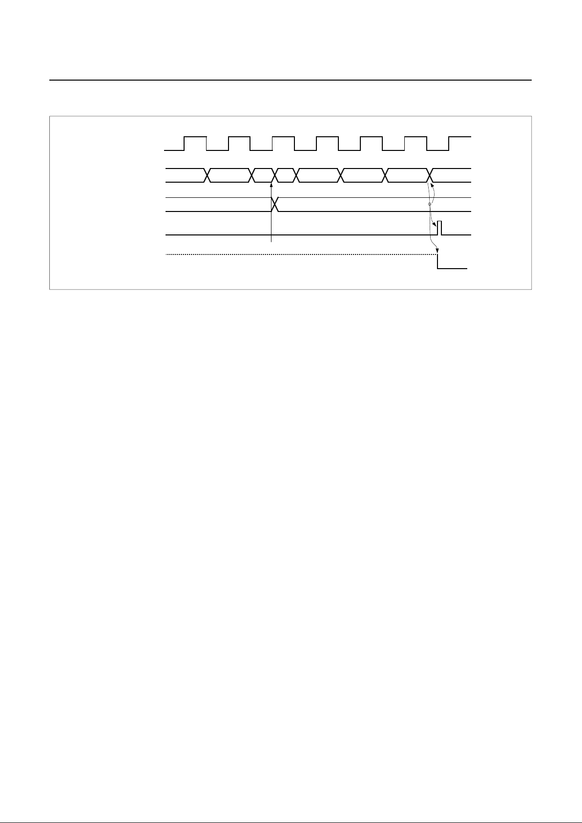
GMS81C4040/87C4060
PRELIMINARY
78
PRELIMINARY
Nov. 1999 Ver 1.0
Figure 20-3 Watchdog ti me r Tim ing
Minimizi ng Current Co nsumption
It should be set properly that curren t flow through po rt
doesn't exist.
First conseide r th e setti ng t o input mode. Be s ure tha t t here
is no current flow after considering its relationship with
external circuit. In input mode, the pin impedance viewing
from external MCU is very high that the current doesn’t
flow.
But input voltage level should be V
SS
or VDD. Be careful
that if unspecified voltage, i.e. if unfirmed voltage level is
applied to input pin, there can be little current (max. 1mA
at around 2V) flow.
If it is not appropriate to set as an input mode, then set to
output mode considering there is no current flow. Setting
to High or Lo w is de cided consi deri ng its rela tio nship wi th
external cir cuit . For ex ample, if th ere is exte rnal p ull-up resistor then it is se t to output mode , i.e . to Hig h, and if there
is external pull-down register, it is set to low. See Figure
20-4 .
2
3
n
Source clock
Binary-counter
WDTR
IFWDT interrupt
WDTR ← "0100_0011b"
10
Match
Detect
Counter
Clear
1
2
30
BIT ov erflow
3
WDT reset reset
Page 83
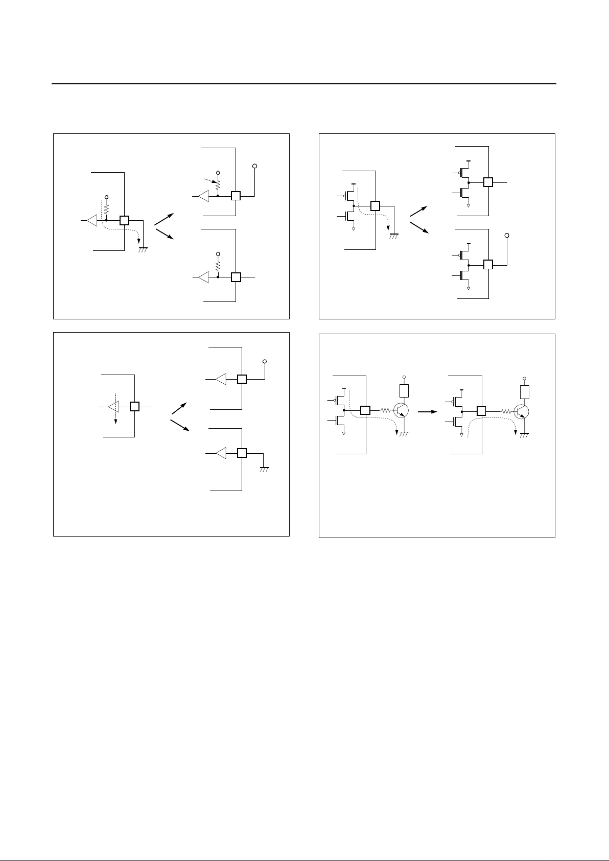
PRELIMINARY
GMS81C4040/87C4060
Nov. 1999 Ver 1.0
PRELIMINARY
79
Figure 20-4 Applicati on exam ple of Port under Power Consumption
INPUT PIN
V
DD
GND
i
V
DD
OUTPUT PIN
GND
i
X
Weak pull-up current flows
In the left case, much current flows from port to GND.
X
ON
OFF
V
DD
internal
pull-up
OUTPUT PIN
GND
i
In the left case, Tr. base current flows from port to GND.
i=0
X
OFF
ON
V
DD
L
ON
OFF
OPEN
GND
V
DD
L
ON
OFF
To avoid power consumption, low output to the port .
INPUT PIN
i
V
DD
X
Very weak current flows
V
DD
O
O
OPEN
ON
OFF
OPEN
i=0
O
O
V
DD
O
i=0
O
GND
O
When port is configured as an input, input level should
be closed to 0V or 5V to avoid power consumption.
Page 84
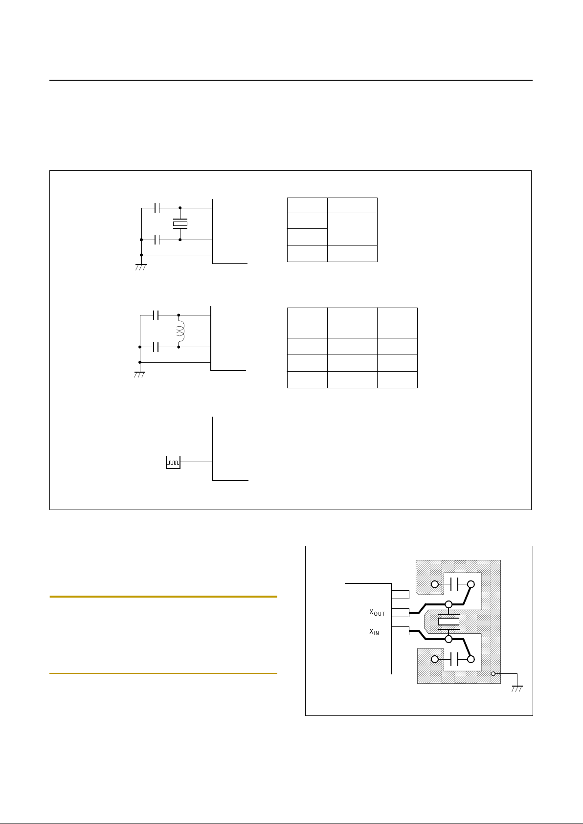
GMS81C4040/87C4060
PRELIMINARY
80
PRELIMINARY
Nov. 1999 Ver 1.0
21. OSCILLATOR CIRCUIT
The GMS81C4040/GMS87C4060 has two oscillation circuits internally. X
IN
and X
OUT
are input an d output for
main frequency and OSC1 a nd OS C2 are input and output
for OSD(On Screen display) frequency, respectively, of a
inverting amplifier which can be configured for use as an
on-chip oscillator, as shown in Figure 21-1 .
Figure 21-1 Oscillation Circuit
Oscillation components have their own characteristics, so
user should consult the component manufacturers for appropriate values of external components.
In addition, see Figure 21-2 for the layout of the crystal.
Note:
Minimize the wir ing length. Do n ot allow wiring to intersect with other signal conductors. Do not allow wiring to
come near changing high current. Set the potential of the
grounding position of the oscillator capacitor to that of V
SS
.
Do not ground to any ground pattern where high current is
present. Do not fetch si gnals from the oscillator.
Figure 21-2 Layout example of Oscillator PCB circuit
X
OUT
X
IN
V
SS
Recommend
C1
C2
X
OUT
X
IN
External Clock
Open
External Oscill ator
LC Oscillator
Crystal Oscillator
fc (MHz)
you have to tune the
For selection L,C valu e ,
OSC2
OSC1
V
SS
frequency to appropriate
range which is dependent
to your target set.
C1
C2
L1
fc (MHz)
10
12
16
C1 & C2 (pF)
30
5
Recommend
fc (MHz)
8
12
16
C1 & C2 (pF)
L (uH)
20
5
20
10
5
100
15
15
15
X
OUT
X
IN
Page 85
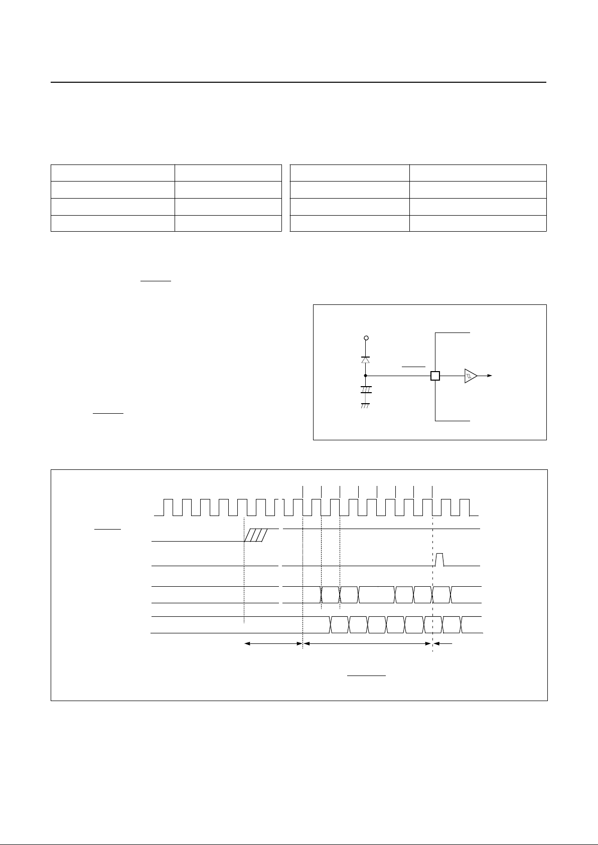
PRELIMINARY
GMS81C4040/87C4060
Nov. 1999 Ver 1.0
PRELIMINARY
81
22. RESET
The GMS81C4040/GMS87C4060 have two types of reset
generation procedures; one is an external reset input, other
is a watch-dog tim er rese t. Tabl e 22-1 shows o n-chip ha rdware initialization by reset action.
Table 22-1 Initial izing Internal Status by Reset Actio n
22.1 External Reset Input
The reset input is the RESET pin, which is the input to a
Schmitt Trigger. A reset in accomplished by holding the
RESET pin low for at least 8 oscillator periods, within the
operating volta ge range and oscillat ion stable, a reset is applie d an d th e int er n al s t at e is ini ti alize d. A f ter reset, 64ms
(at 4 MHz) add w ith 7 oscillator periods are required to
start execution as shown in Figure 22-2 .
Internal RAM is not affect ed by reset. When V
DD
is turned
on, the RAM content is indeterminate. Therefore, this
RAM should be initialized before reading or testing it.
When the RESET
pin input goes high, the reset operation
is released and the program execution starts at the vector
address stored at addresse s FFFE
H
- FFFFH.
A connecting for simple power-on-reset is s hown in Figure
22-1 .
Figure 22-1 Simple Power-on-Reset Circuit
Figure 22-2 Timing Diagram after RESET
On-chip Hardware Initial Value On-chip Hardware Initial Value
Program counter PC
(FFFF
H
) - (FFFEH)
Peripheral clock Off
RAM page register DPGR
00
H
Watchdog timer Disable
G-flag of PSW G 0 Control registers Refer to Table 8-1 on page 22
RESET
+
−
V
DD
GND
MCU
MAIN PROGRAM
Oscillator
(X
IN
pin)
?
?
FFFE FFFF
Stabilization Time
t
ST
= 62.5mS at 4.19MHz
RESET
ADDRESS
DATA
1 2 3 4 5 6 7
??
Start
?
??
FE?ADL
ADH
OP
BUS
BUS
RESET Process Step
~
~
~
~
~
~
~
~
~
~
~
~
t
ST
= x 256
f
MAIN
÷1024
1
Fetch
~
~
Page 86

GMS81C4040/87C4060
PRELIMINARY
82
PRELIMINARY
Nov. 1999 Ver 1.0
22.2 Watchdog Timer Reset
Refer to “20. WATCHDOG TIMER” on page 76.
Page 87

PRELIMINARY
GMS81C4040/87C4060
Nov. 1999 Ver 1.0
PRELIMINARY
83
23. OTP Programming
23.1 GMS87C4060 OTP Programming
You can burn out GMS87C4060 OTP through the gen eral
Gang programmer using Intel 27010/C010 mode. In Devleopment tool pa ckage auxil iar y, GMS87C40 60-to -2701 0/
C010 conversion socket is included. GMS87C4060 have
two ROM memory areas. One is Program ROM memory
and the other is Font ROM memory. Progra m ROM a rea is
from 1000h to FFFFh Font ROM area is from 10000h to
13FFFh. When you acquire new OTP, actually, the OTP is
not fully blank. The OPT have six test pattern in the OSD
Font ROM memory(see figure23-1). The test pattern are
written at 11FA0h ~ 11FFFh and 13FA0h ~ 13FFFh.
Note:
DO NOT wr ite any data in this area(11FA0h ~
11FFFh, 13FA0h ~ 13FFFh)
Blank Check
If you run bla nk check fun ction of ROM write r, ROM
writer inform blank error be ca use of test pattern. To avoid
this situation, you must run the blank check function seperetely. For example, check OTP address rage of 1000h ~
11F9Fh at first. And then check OPT address range of
12000h ~ 13F9Fh. If you have ROM writer wit hout part ia l
blank check function, please do not run blank check function.
Figure 23-1 GMS87C4060 OTP Memory Map
Program Writing
There are two kind of OTP file. One is program OT P
file(** *.OTP) and th e other is font OTP file(*** .FNT).
You can make each file through ASMLINKER.exe and
OSDFONT.exe respectively. All OTP file is Motolora Sformat. You can burn the p rogra m file and font fi le respe ctively or together. To burn program file and font file respectively, refe r following procedure
1. Make pro gram OTP file and f ont OTP file repe ctively.
2. Check whether six test pattern is included in font
OTP file(see below Six Text Pattern)
3. Burn program OTP file(Set chip target addres s
1000h ~ FFFFh)
4. Burn font OTP file(Set chip target address 10000h
~13FFFh)
Note:
When you pro gram the OTP fil e, DO NOT check the
blank. Because there are already written data(Six test pattern / 11FA0h ~ 11FFF h, 13FA0h~13 FFFh) It w ill occur
blank error
To burn program fil e and font fil e toge ther, refer f oll owing
procedure
1. Add program OTP file and font OTP file
2. Check whether six test pattern is included in font
OTP file(see below Six Text Pattern)
3. Burn OTP file(Set chip target address 1000h ~
13FFFh)
About other details, re fer ROM wirter manual.
Six Test Patte rn
When you make font file through OSDFONT.exe, please
confirm whether six test patte rn is inc luded or not in character addres s 1FAh ~ 1FFh, T o include six test p atern, refer
following procedure.
1. Make Font file and save it to your PC
2. Reopen the font file and save it to your HDD once
again.
3. Then six test pattern will be included automatically.
(Character address 1FAh ~ 1FFh)
1000H
FFFFH
13FFFH
OSD Font
Memory
Program
Memory
Page 88
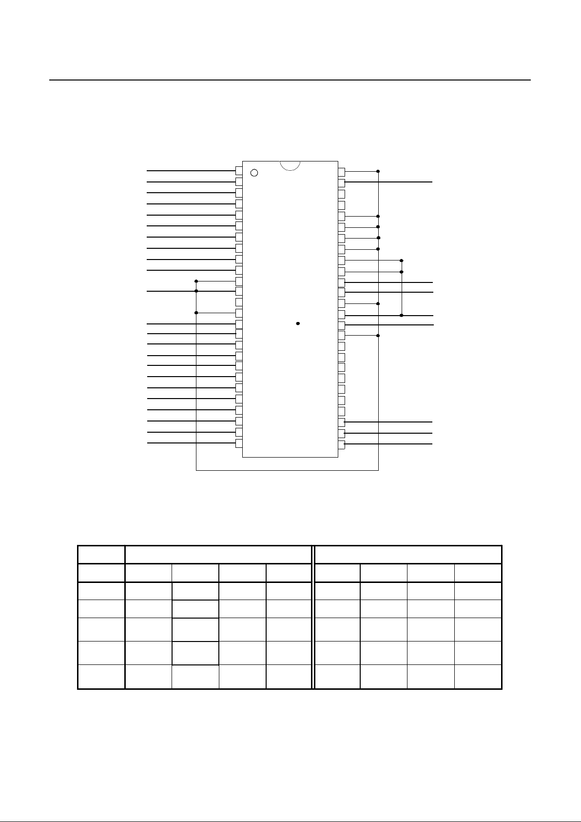
GMS81C4040/87C4060
PRELIMINARY
84
PRELIMINARY
Nov. 1999 Ver 1.0
23.2 .Device configuration data
Figure 23-2 Figure Pin Confi guration in OTP Programming Mode
Figure 23-3 Figure Mode Table
HYUNDAI
GMS874060
A15
A14
A13
A12
A11
A10
A9
A8
A7
A6
A3
A2
A1
A0
O7
O6
O5
O4
O3
A16
A4
A5
GND
CEB
PGMB
OEB
V
CC
V
PP
O0
O1
O2
1
2
3
4
5
6
7
8
9
10
11
12
13
14
15
16
17
18
19
20
21
22
23
24
25
26
52
51
50
49
48
47
46
45
44
43
42
41
40
39
38
37
36
35
34
33
32
31
30
29
28
27
GMS87C4060 Intel 27010
Mode VPP CEB OEB PGMB VPP CEB OEB PGMB
Program 12.75V Low High
*2
Low
*1
12.75V Low High Low
Verify 12.75V Low Low High 12.75V Low Low High
Optional
Ver i fy
5V Low Low X 5V Low Low X
Gang
Write
*3
12.75V Low High Low 12. 75V Low High Low
Gang
Verify
*4
12.75V,
5V
Low Low X 12.75V Low Low X
Page 89
PRELIMINARY
GMS81C4040/87C4060
Nov. 1999 Ver 1.0
PRELIMINARY
85
*1: Low = Input Low Voltage = VIL(<0.8V)
*2: High = Input High Value = VIL(>2.0V)
*3: In Gang Write Mode, All OTPs are programmed sim-
ulaneously. So all signals of OTPs are in the same condition
*4: In Gang Verify mode, the VPP pin can be sset to both
normal high(5V), aand 12.75V and chip slecection is possible using the CEB pin
Figure 23-4 Figure AC Programming Characteristics
LimitsSYMBOL Parameter
Min Typ Max Unit
Conditions
tAS Address Setup Time 2
µ
s
tOES OEB Setup Time 2
µ
s
tDS Data Setup Time 2
µ
s
tAH Address Hold Time 0
µ
s
tDH Data Hold Time 2
µ
s
tDFP OEB High to Output Float Delay 0 130 ns Note1
tVPS Vpp Setup Time 2
µ
s
tCES CEB Setup Time 2
µ
s
tPW PGMB in i tial program pulse width 95 100 105
µ
s
Quick pulse
programming
tOE Data Valid from OEB 100 ns
tACC Address to output delay 150 ns
tOH out pu t hol d from ad dr e ss es C E B or
OEB whichever occurrs first
00ns
tCE CEB to output delay 100 ns
tCS chip selection interval
(@Gang verify)
100 ns
*Note1: Output Float is defined as the point where data is no longer driven
Page 90
GMS81C4040/87C4060
PRELIMINARY
86
PRELIMINARY
Nov. 1999 Ver 1.0
Figure 23-5 Pin Mapping Table between Intel 27010/C010 and GMS87C4060
Intel 27010 GMS87C4060
Pin Name Pin Number Pin Name Pin Number
VPP 1 TEST_ N 38
A16 2 R67 26
A153R271
A124R244
A7 5 R17 9
A6 6 R16 10
A5 7 R15 15
A4 8 R14 16
A3 9 R13 17
A2 10 R12 18
A1 11 R11 19
A0 12 R10 20
O0 13 R00 29
O1 14 R01 28
O2 15 R02 27
GND 16 VSS 12, 40
O3 17 R03 25
O4 18 R04 24
O5 19 R05 23
O6 20 R06 22
O7 21 R07 21
CEB 22 R41 51
A10 23 R22 6
OEB 24 R53 41
A11 25 R23 5
A9 26 R21 7
A8 27 R20 8
A13 28 R25 3
A14 29 R26 2
N.C. 30
PGMB 31 R52 42
VCC 32 VDD 39
Page 91
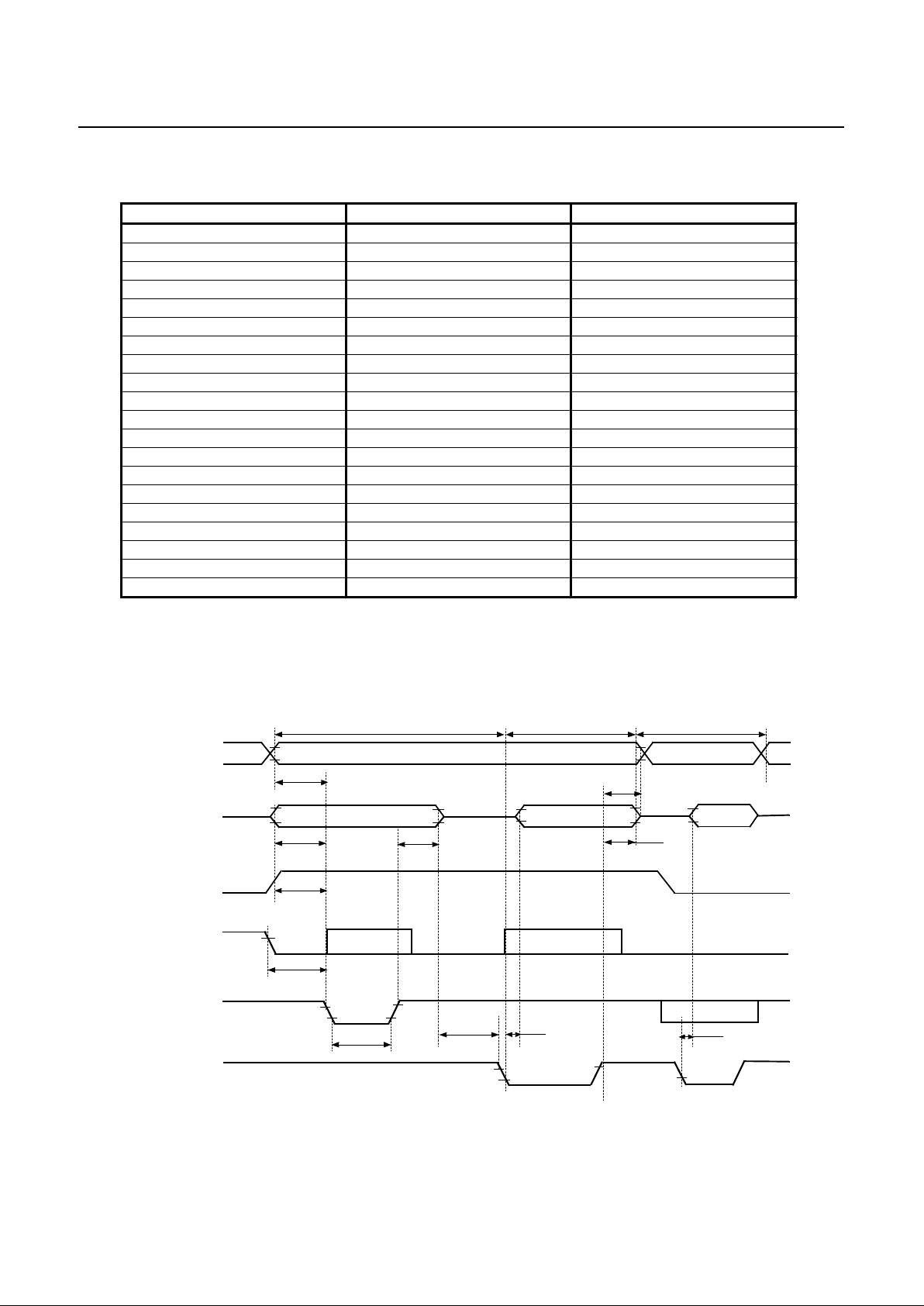
PRELIMINARY
GMS81C4040/87C4060
Nov. 1999 Ver 1.0
PRELIMINARY
87
Figure 23-6 Connection of Othe r Pins of GMS87C4060 in OTP Mode
23.3 Timing Chart
Figure 23-7 Figure Programming Timing Chart
Pin Name Pin Number Connect to
RESET_N 11 GND
Xout 13 Not Connect
Xin 14 GND
R 30 Not Connect
G 31 Not Connect
B 32 Not Connect
R56 33 Not Conne ct
R55 34 Not Conne ct
R54 35 Not Conne ct
OSC2 36 Not Connect
OSC1 37 GND
R47 45 GND
R46 46 GND
R45 47 GND
R44 48 GND
R43 4 9 Not C onne c t
R42 5 0 Not C onne c t
R40 52 GND
R50 44 VDD
R51 43 VDD
Address
VPP
Data in Stable
CEB
Data
PGMB
OEB
V
IH
V
IL
V
IH
V
IL
12.5V
5V
V
IH
V
IL
Data out Valid
Valid ouput
V
IH
V
IL
V
IH
V
IL
Address Stable
Program Verify Optinal Verify
Address Valid
tAS
tDS
tDH
tVPS
tAH
tDFP
tCES
tPW
tOES
tOE
tOE
High
Z
Don’t care
Don’t care
Don’t care
Page 92
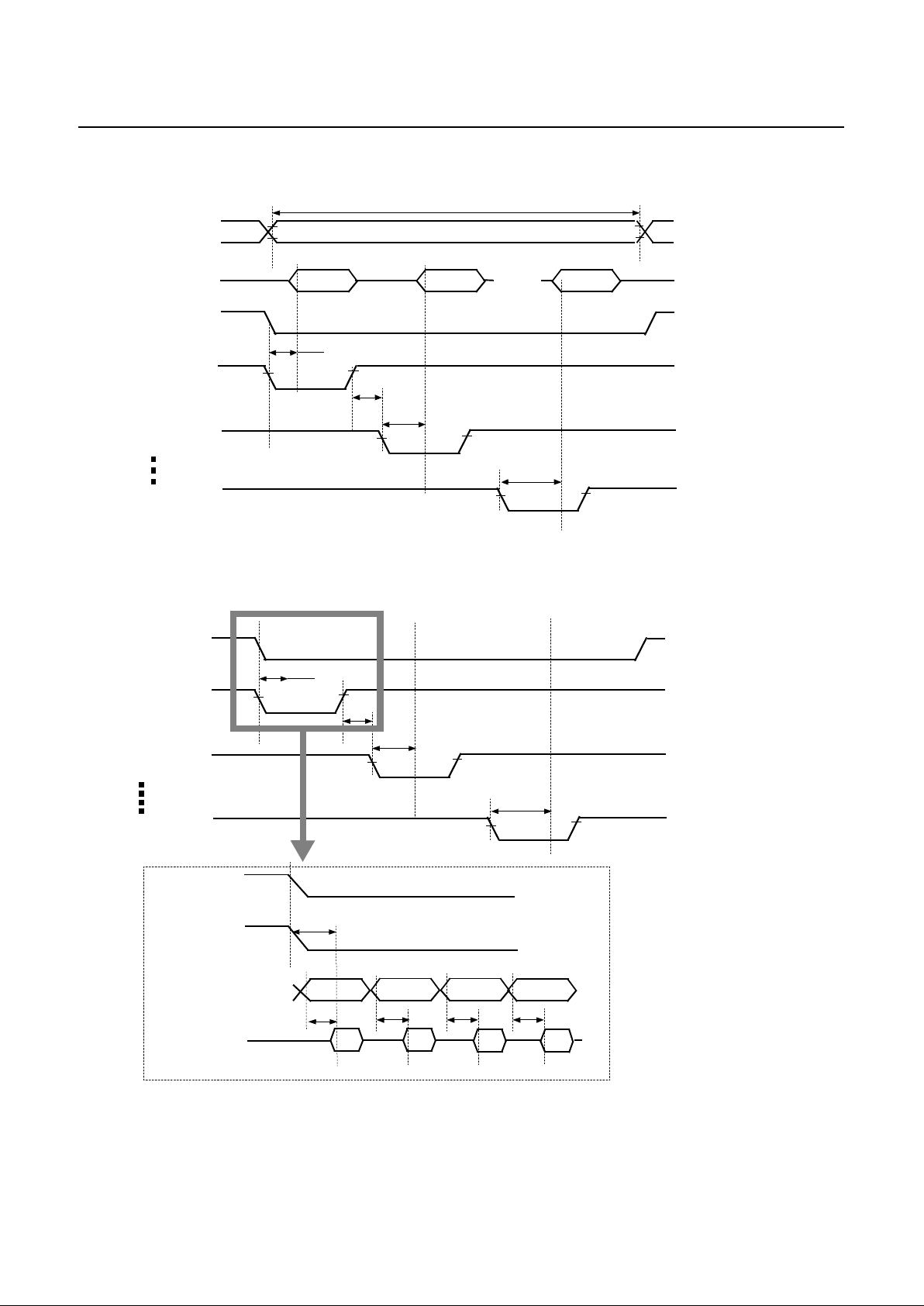
GMS81C4040/87C4060
PRELIMINARY
88
PRELIMINARY
Nov. 1999 Ver 1.0
Figure 23-8 AC Wave Form in Gang Verify Mode
Address
OEB
Data
CEB[0]
V
IH
V
IL
V
IH
V
IL
V
IH
V
IL
V
IH
V
IL
Address Stable
Optinal Verify
0th OTP
1st OTP
Data DataData
.....
tACC
(n-1)th OTP
CEB[1]
V
IH
V
IL
tCS
tACC
CEB[n-1]
V
IH
V
IL
tACC
1) When you verify the data in the same address of many OTPs.
When you select OTPs using CEB, and can verify the data inthe same address.
(PGMB : Don’t care , Vpp : V
IH
or 12.5V )
OEB
CEB[0]
V
IH
V
IL
V
IH
V
IL
tACC
CEB[1]
V
IH
V
IL
tCS
tACC
CEB[n-1]
V
IH
V
IL
tACC
OEB
CEB[0]
V
IH
V
IL
V
IH
V
IL
tACC
Addr0
Addr2
Addr3
Addr1
Data0 Data1 Data2
Data3
tACC
tACC tACC tACC
Data
Address
V
IH
V
IL
V
IH
V
IL
2) When you verify the data in s si ngle OTP throughout the ROM address
Page 93

PRELIMINARY
GMS81C4040/87C4060
Nov. 1999 Ver 1.0
PRELIMINARY
89
24. Assemble mnemonics
24.1 Instruction Map
0000000000010100010020001103001000400101050011006001110701000080100109010100A010110B011000C011010D011100E01111
0F
000
NOP
SET1
dp.bit
BBS
A.bit,rel
BBS
dp.bit,rel
ADC
#imm
ADCdpADC
dp+X
ADC
!abs
ASLAASLdpTCALL
0
SETA1
.bit
BITdpPOPAPUSH
A
BRK
001
CLRC
// // //
SBC
#imm
SBC
dp
SBC
dp+X
SBC
!abs
ROLAROLdpTCALL2CLRA1
.bit
COMdpPOP
X
PUSH
X
BRA
rel
010
CLRG
// // //
CMP
#imm
CMPdpCMP
dp+X
CMP
!abs
LSRALSRdpTCALL4NOT1
M.bit
TSTdpPOPYPUSHYPCALL
Upage
011
DI
// // //
OR
#immORdpORdp+XOR!abs
RORARORdpTCALL
6
OR1
OR1B
CMPX
dp
POP
PSW
PUSH
PSW
RET
100
CLRV
// // //
AND
#imm
ANDdpAND
dp+X
AND
!abs
INCAINCdpTCALL
8
AND1
AND1B
CMPY
dp
CBNE
dp+X
TXSP
INC
X
101
SETC
// // //
EOR
#imm
EORdpEOR
dp+X
EOR
!abs
DECADECdpTCALL
10
EOR1
EOR1B
DBNE
dp
XMA
dp+X
TSPX
DEC
X
110
SETG
// // //
LDA
#imm
LDAdpLDA
dp+X
LDA
!abs
TXA
LDY
dp
TCALL
12
LDC
LDCB
LDX
dp
LDX
dp+Y
XCN DAS
111
EI
// // //
LDM
dp,#imm
STAdpSTA
dp+X
STA
!abs
TAX
STY
dp
TCALL14STC
M.bit
STXdpSTX
dp+Y
XAS
10000
10
100011110010121001113101001410101151011016101111711000181100119110101A110111B111001C111011D111101E11111
1F
000
BPL
rel
CLR1
dp.bit
BBC
A.bit,rel
BBC
dp.bit,rel
ADC
{X}
ADC
!abs+Y
ADC
[dp+X]
ADC
[dp]+Y
ASL
!abs
ASL
dp+X
TCALL
1
JMP
!abs
BIT
!abs
ADDWdpLDX
#imm
JMP
[!abs]
001
BVC
rel
// // //
SBC
{X}
SBC
!abs+Y
SBC
[dp+X]
SBC
[dp]+Y
ROL
!abs
ROL
dp+X
TCALL3CALL
!abs
TEST
!abs
SUBW
dp
LDY
#imm
JMP
[dp]
010
BCC
rel
// // //
CMP
{X}
CMP
!abs+Y
CMP
[dp+X]
CMP
[dp]+Y
LSR
!abs
LSR
dp+X
TCALL
5
MUL
TCLR1
!abs
CMPWdpCMPX
#imm
CALL
[dp]
011
BNE
rel
// // //
OR
{X}OR!abs+YOR[dp+X]OR[dp]+Y
ROR
!abs
ROR
dp+X
TCALL7DBNE
Y
CMPX
!abs
LDYAdpCMPY
#imm
RETI
100
BMI
rel
// // //
AND
{X}
AND
!abs+Y
AND
[dp+X]
AND
[dp]+Y
INC
!abs
INC
dp+X
TCALL
9
DIV
CMPY
!abs
INCWdpINC
Y
TAY
101
BVS
rel
// // //
EOR
{X}
EOR
!abs+Y
EOR
[dp+X]
EOR
[dp]+Y
DEC
!abs
DEC
dp+X
TCALL11XMA
{X}
XMAdpDECWdpDEC
Y
TYA
110
BCS
rel
// // //
LDA
{X}
LDA
!abs+Y
LDA
[dp+X]
LDA
[dp]+Y
LDY
!abs
LDY
dp+X
TCALL13LDA
{X}+
LDX
!abs
STYA
dp
XAY DAA
111
BEQ
rel
// // //
STA
{X}
STA
!abs+Y
STA
[dp+X]
STA
[dp]+Y
STY
!abs
STY
dp+X
TCALL15STA
{X}+
STX
!abs
CBNE
dp
XYX NOP
Page 94
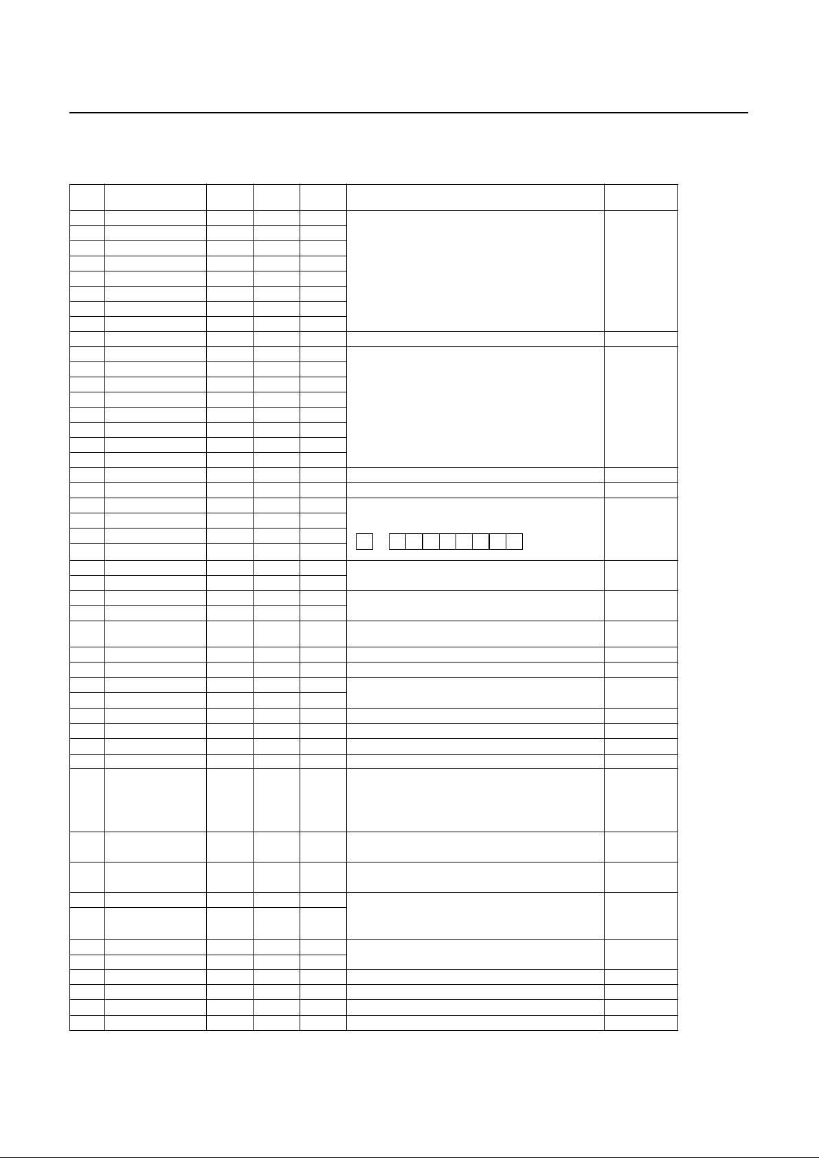
GMS81C4040/87C4060
PRELIMINARY
90
PRELIMINARY
Nov. 1999 Ver 1.0
24.2 Alphabetic order table of instruction
NO. MNENONIC
OP
CODE
BYTE
NO.
CYCLE
NO
OPERATION
FLAG
NVGBHIZC
1 ADC #imm 04 2 2 Add with carry.
NV - - H - ZC
2 ADC dp 05 2 3
A
←
A + (M) + C
3 ADC dp + X 06 2 4
4 ADC !abs 07 3 4
5 ADC !abs+Y 15 3 5
6 ADC [dp+X] 16 2 6
7 ADC [dp]+Y 17 2 6
8 ADC {X} 14 1 3
9 ADDW dp 1D 2 5 16-bits add without carry : YA
←
YA + (dp+1)(d p) NV - - H - ZC
10 AND #imm 84 2 2 Logical AND
N - - - - - Z -
11 AND dp 85 2 3
A
←
A ^ (M)
12 AND dp + X 86 2 4
13 AND !abs 87 3 4
14 AND !abs+Y 95 3 5
15 AND [dp+X] 96 2 6
16 AND [dp] + Y 97 2 6
17 AND {X} 94 1 3
18 AND1 M.bit 8B 3 4 Bit AND C-flag : C
←
C ^ (M.bit) - - - - - - - C
19 AND1B M.bit 8B 3 4 Bit AND C-flag and NOT : C
←
C ^ ~(M.bit) - - - - - - - C
20 ASL A 08 1 2 Arithmetic shift left
N - - - - - ZC
21 ASL dp 09 2 4
22 ASL dp + X 19 2 5
23 ASL !abs 18 3 5
24 BBC A.bit,rel y2 2 4/6 Branch if bit clear :
- - - - - - - -
25 BBC dp.bit,rel y3 3 5/7 if(bit) = 0, then PC
←
PC + rel
26 BBS A.bit,rel x2 2 4/6 Branch if bit clear :
- - - - - - - -
27 BBS dp.bit,rel x3 3 5/7 if(bit) = 1, then PC
←
PC + rel
28 BCC rel 50 2 2/4
Branch if carry bit clear :
if(C) = 0, then PC
←
PC + rel
MM - - - - Z -
29 BCS rel D0 2 2/4 Branch if carry bit set : If (C) =1, then PC
←
PC + rel - - - - - - - -
30 BEQ rel F0 2 2/4 Branch if equal : if (Z) = 1, then PC
←
PC + rel - - - - - - - -
31 BIT dp 0C 2 4 Bit test A with memory :
MM - - - - Z -
32 BIT !abs 1C 3 5
Z ← A ^ M, N
←
(M
7
), V
←
(M
6
)
33 BMI rel 90 2 2/4 Branch if munus : if (N) = 1, then PC
←
PC + rel - - - - - - - -
34 BNE rel 70 2 2/4 Branch if not equal : if (Z) = 0, then PC
←
PC + rel - - - - - - - -
35 BPL rel 10 2 2/4 Branch if not minus : if (N) = 0, then PC
←
PC + rel - - - - - - - -
36 BRA rel 2F 2 4 Branch always : PC
←
PC + rel - - - - - - - -
37 BRK 0F 1 8 Software interrupt:
- - - 1 - 0 - -
B
←
“1”, M(SP)
←
(PC
H
), SP ← SP - 1,
M(s)
←
(PC
L
), SP ← S - 1, M(SP) ← PSW,
SP
←
SP - 1, PC
L
←
(0FFDE
H
), PCH ← (0FFDFH)
38 BVC rel 30 2 2/4 Branch if overflow bit clear :
- - - - - - - -
If (V) = 0, then PC
←
PC + rel
39 BVS rel B0 2 2/4 Branch if overflow bit set :
- - - - - - - -
If (V) = 1, then PC
←
PC + rel
40 CALL !abs 3B 3 8 Subroutine call
- - - - - - - -
41 CALL [dp] 5F 2 8
M(SP)
←
(PC
H
), SP ← SP-1, M(SP)
←
(PC
L
), SP←SP-1
if !abs, PC
←
abs ; if [dp], PC
L
←
(dp), PC
H
← (dp+1)
42 CBNE dp,rel FD 3 5/7 Compare and branch if not equal ;
- - - - - - - -
43 CBNE dp + X, rel 8D 3 6/8 If A ≠ (M), then PC
←
PC + rel.
44 CLR1 dp.bit y1 2 4 Clear bit : (M.bit)
←
“0” - - - - - - - -
45 CLR1A A.bit 2B 2 2 Clear A.bit : (A.bit)
←
“0” - - - - - - - -
46 CLRC 20 1 2 Clear C-flag : C
←
“0” - - - - - - - 0
47 CLRG 40 1 2 Clear G-flag : G
←
“0” - - 0 - - - - -
C 7 6 5 4 3 2 1 0
← ← ← ← ← ← ← ← ← ← "0
"
Page 95
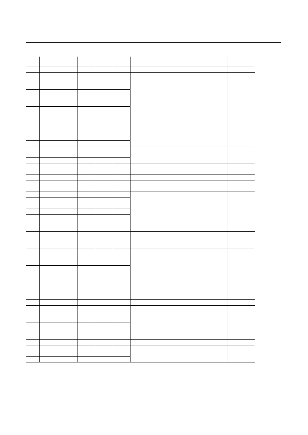
PRELIMINARY
GMS81C4040/87C4060
Nov. 1999 Ver 1.0
PRELIMINARY
91
48 CLRV 80 1 2 Clear V-flag : V ← “0” - 0 - - 0 - - 49 CMP #imm 44 2 2 Compare accumulator contents with memory contents
N - - - - - ZC
50 CMP dp 45 2 3 A - (M)
51 CMP dp + X 46 2 4
52 CMP !abs 47 3 4
53 CMP !abs + Y 55 3 5
54 CMP [dp + X] 56 2 6
55 CMP [dp] + Y 57 2 6
56 CMP {X} 54 1 3
57 CMPW dp 5D 2 4 Compare YA contents with memory pair contents : N - - - - - ZC
YA - (dp+1)(dp)
58 CMPX #imm 5E 2 2 Compare X contents with memory contents
N - - - - - ZC59 CMPX dp 6C 2 3 X - (M)
60 CMPX !abs 7C 3 4
61 CMPY #imm 7E 2 2 Compare Y contents with memory contents
N - - - - - ZC62 CMPY dp 8C 2 3 Y - (M)
63 CMPY !abs 9C 3 4
64 COM dp 2C 2 4 1’s complement : (dp)
←
~(dp) N - - - - - Z 65 DAA DF 1 3 Decimal adjust for addition N - - - - - ZC
66 DAS CF 1 3 Decimal adjust for substraction N - - - - - ZC
67 DBNE dp,rel AC 3 5/7 Decrement and branch if not equal :
- - - - - - - -
68 DBNE Y,rel 7B 2 4/6 if (M) ≠ 0, then PC
←
PC + rel.
69 DEC A A8 1 2 Decrement
N - - - - - Z -
70 DEC dp A9 2 4 M
←
M - 1
71 DEC dp + X B9 2 5
72 DEC !abs B8 3 5
73 DEC X AF 1 2
74 DEC Y BE 1 2
75 DECW dp BD 2 6 Decrement memory pair : (dp+1)(dp)
←
{(dp+1)(dp)} - 1 N - - - - - Z -
76 DI 60 1 3 Disable interrupts : I
←
“0” - - - - - 0 - -
77 DIV 9B 1 12 Divide : YA/A
←
Q:A, R:Y NV - - H - Z -
78 EI E0 1 3 Enable interrupts : I
←
“1” - - - - - 1 - -
79 EOR #imm A4 2 2 Exclusive OR
N - - - - - Z -
80 EOR dp A5 2 3 A
←
A ⊕ (M)
81 EOR dp + X A6 2 4
82 EOR !abs A7 3 4
83 EOR !abs + Y B5 3 5
84 EOR [ dp + X] 96 2 6
85 EOR [dp] + Y 97 2 6
86 EOR {X} 94 1 3
87 EOR1 M.bit AB 3 5 Bit exclusive-OR C-flag : C
←
C ⊕ (M.bit) - - - - - - - C
88 EOR1B M.bit AB 3 5 Bit exclusive-OR C-flag and NOT : C
←
C
⊕ ∼
(M.bit) - - - - - - - C
89 INC A 88 1 2 Increment N - - - - - ZC
90 INC dp 89 2 4 (M)
←
(M) + 1
N - - - - - Z -
91 INC dp + X 99 2 5
92 INC !abs 98 3 5
93 INC X 8F 1 2
94 INC Y 9E 1 2
95 INCW dp 9D 2 6 Increment memory pair : (dp+1)(dp)
←
{(dp+1)(dp)} + 1 N - - - - - Z -
96 JMP !abs 1B 3 3 Unconditional jump
- - - - - - - -97 JMP [!abs] 1F 3 5 PC
←
jump address
98 JMP [dp] 3F 2 4
NO. MNENONIC
OP
CODE
BYTE
NO.
CYCLE
NO
OPERATION
FLAG
NVGBHIZC
Page 96
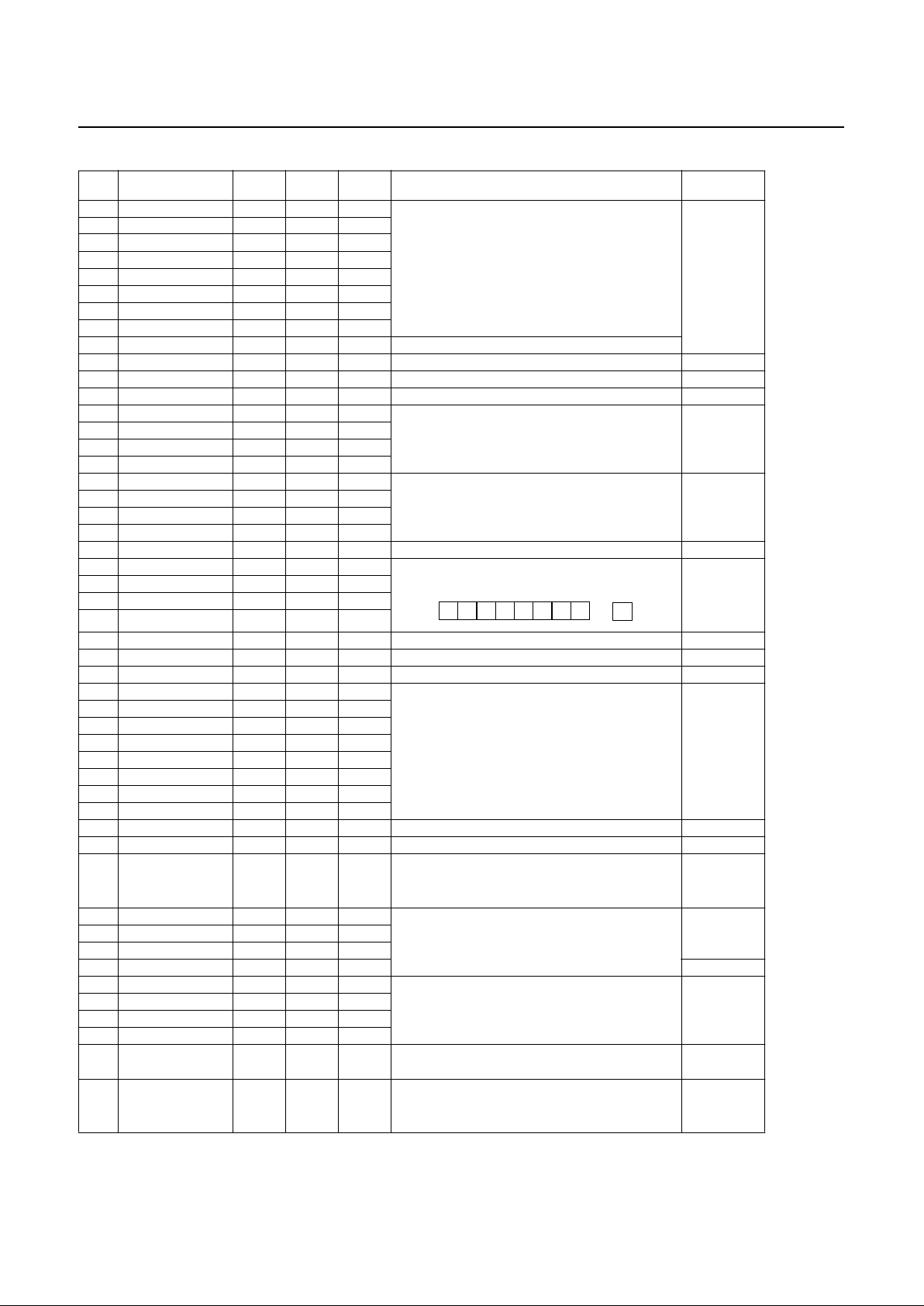
GMS81C4040/87C4060
PRELIMINARY
92
PRELIMINARY
Nov. 1999 Ver 1.0
99 LDA #imm C4 2 2 Load accumulator
N - - - - - Z -
100 LDA dp C5 2 3 A
←
(M)
101 LDA dp + X C6 2 4
102 LDA !abs C7 3 4
103 LDA !abs + Y D5 3 5
104 LDA [dp + X] D6 2 6
105 LDA [dp]+Y D7 2 6
106 LDA {X} D4 1 3
107 LDA {X}+ DB 1 4 X-register auto-increment : A
←
(M), X ← X + 1
108 LDC M.bit CB 3 4 Load C-flag : C
←
(M.bit) - - - - - - - C
109 LDCB M.bit CB 3 4 Load C-flag with NOT : C
←
~(M.bit) - - - - - - - C
110 LDM dp,#imm E4 3 5 Load memory with immediate data : (M)
←
imm - - - - - - - -
111 LDX #imm 1E 2 2 Load X-register
N - - - - - Z -
112 LDX dp CC 2 3 X
←
(M)
113 LDX dp + Y CD 2 4
114 LDX !abs DC 3 4
115 LDY #imm 3E 2 2 Load X-register
N - - - - - Z -
116 LDY dp C9 2 3 Y
←
(M)
117 LDY dp + Y D9 2 4
118 LDY !abs D8 3 4
119 LDYA dp 7D 2 5 Load YA : YA
←
(dp+1)(dp) N - - - - - Z -
120 LSR A 48 1 2 Logical shift right
N - - - - - ZC
121 LSR dp 49 2 4
122 LSR dp + X 59 2 5
123 LSR !abs 58 3 5
124 MUL 5B 1 9 Multiply : YA
←
Y x A N - - - - - Z 125 NOP 00,FF 1 2 No operation - - - - - - - 126 NOT1 M.bit 4B 3 5 Bit complement : (M.bit)
←
~(M.bit) - - - - - - - -
127 OR #imm 64 2 2 Logical OR
N - - - - - Z -
128 OR dp 65 2 3 A
←
A V (M)
129 OR dp + X 66 2 4
130 OR !abs 67 3 4
131 OR !abs + Y 75 3 5
132 OR [dp +X} 76 2 6
133 OR [dp] + Y 77 2 6
134 OR {X} 74 1 3
135 OR1 M.bit 6B 3 5 Bit OR C-flag : C
←
C V (M.bit) - - - - - - - C
136 OR1B M.bit 6B 3 5 Bit OR C-flag and NOT : C
←
C V ~(M.bit) - - - - - - - C
137 PCALL 4F 2 6
U-page call : M(SP)
←
(PC
H
), SP
←
SP -1,
- - - - - - - -
M(SP)
←
(PC
L
), SP
←
SP -1,
PC
L
←
(upage), PC
H
←
"OFF
H
"
138 POP A 0D 1 4 Pop from stack
- - - - - - - -139 POP X 2D 1 4 SP
←
SP + 1, Reg. ← M(SP)
140 POP Y 4D 1 4
141 POP PSW 6D 1 4 (restored)
142 PUSH A 0E 1 4 Push to stack
- - - - - - - -
143 PUSH X 2E 1 4 M(SP)
←
Reg. SP ← SP - 1
144 PUSH Y 4E 1 4
145 PUSH PSW 6E 1 4
146 RET 6F 1 5 Return from subroutine :
- - - - - - - -
SP ← SP+1, PC
L
← M(SP), SP ← SP+1, PCH ← M(SP)
147 RETI 7F 1 6 Return from interrupt :
(restored)
SP ← SP+1, PSW ← M(SP), SP ← SP+1,PC
L
← M(SP),
SP ← SP+1, PC
H
← M(SP)
NO. MNENONIC
OP
CODE
BYTE
NO.
CYCLE
NO
OPERATION
FLAG
NVGBHIZC
7 6 5 4 3 2 1 0 C
"0"
→ → → → → → → → → →
Page 97
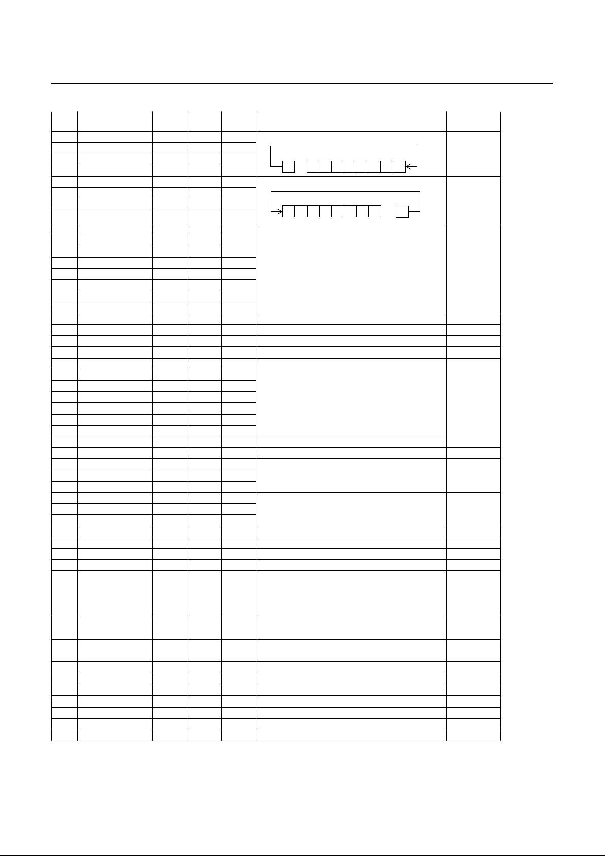
PRELIMINARY
GMS81C4040/87C4060
Nov. 1999 Ver 1.0
PRELIMINARY
93
148 ROL A 28 1 2 Rotate left through carry
N - - - - - ZC
149 ROL dp 29 2 4
150 ROL dp + X 39 2 5
151 ROL !abs 38 3 5
152 ROR A 68 1 2 Rotate right through carry
N - - - - - ZC
153 ROR dp 69 2 4
154 ROR dp + X 79 2 5
155 ROR !abs 78 3 5
156 SBC #imm 24 2 2 Substract with carry
NV - - HZC
157 SBC dp 25 2 3 A ← A - (M) - ~(C)
158 SBC dp + X 26 2 4
159 SBC !abs 27 3 4
160 SBC !abs + Y 35 3 5
161 SBC [dp + X] 36 2 6
162 SBC [dp] + Y 37 2 6
163 SBC {X} 34 1 3
164 SET1 dp.bit x1 2 4 Set bit : (M.bit) ← “1” - - - - - - - 165 SETA1 A.bit 0B 2 2 Set A.bit : (A.bit) ← “1” - - - - - - - 166 SETC A0 1 2 Set C-flag : C ← “1” - - - - - - - 1
167 SETG C0 1 2 Set G-flag : G ← “1” - - 1 - - - - 168 STA dp E5 2 3 Store accumulator contents in memory
- - - - - - - -
169 STA dp + X E6 2 4 (M) ← A
170 STA !abs E7 3 4
171 STA !abs + Y F5 3 5
172 STA [dp + X] F6 2 6
173 STA [dp] + Y F7 2 6
174 STA {X} F4 1 3
175 STA {X}+ FB 1 4 X-register auto-increment : (M) ← A, X ← X + 1
176 STC M.bit EB 3 6 Store C-flag : (M.bit) ← C - - - - - - - 177 STX dp EC 2 4 Store X-register contents in memory
- - - - - - - -178 STX dp + Y ED 2 5 (M) ← X
179 STX !abs FC 3 5
180 STY dp E9 2 4 Store Y-register contents in memory
- - - - - - - -181 STY dp + X F9 2 5 (M) ← Y
182 STY !abs F8 3 5
183 STYA dp DD 2 5 Store YA : (dp+1)(dp) ← YA - - - - - - - 184 SUBW dp 3D 2 5 16-bits substract without carry : YA ← YA - (dp+1)(dp) NV - - H - ZC
185 TAX E8 1 2 Transfer accumulator contents to X-register : X ← A N - - - - - Z 186 TAY 9F 1 2 Transfer accumulator contents to Y-register : Y ← A N - - - - - Z 187 TCALL n nA 1 8 Table call :
- - - - - - - -
M(SP) ← (PC
H
), SP ← SP -1,
M(SP) ← (PC
L
), SP ← SP -1
PC
L
← (Table vector L), PCH ← (Table vector H)
188 TCLR1 !abs 5C 3 6
Test and clear bits with A :
N - - - - - Z -
A - (M), (M) ← (M) ^ ~(A)
189 TSET1 !abs 3C 3 6
Test and set bits with A :
N - - - - - Z -
A - (M), (M) ← (M) V (A)
190 TSPX AE 1 2
Transfer stack-pointer contents to X-register : X
← SP N - - - - - Z -
191 TST dp 4C 2 3
Test memory contents for negative or zero : (dp) - 00
H
N - - - - - Z 192 TXA C8 1 2 Transfer X-register contents to accumulator : A ← X N - - - - - Z 193 TXSP 8E 1 2 Transfer X-register contents to stack-pointer : SP ← X N - - - - - Z 194 TYA BF 1 2 Transfer Y-register contents to accumulator : A ← Y N - - - - - Z 195 XAX EE 1 4 Exchange X-register contents with accumulator : X fA - - - - - - - 196 XAY DE 1 4 Exchange Y-register contents with accumulator : Y fA - - - - - - - -
NO. MNENONIC
OP
CODE
BYTE
NO.
CYCLE
NO
OPERATION
FLAG
NVGBHIZC
C 7 6 5 4 3 2 1 0
← ← ← ← ← ← ← ← ←
7 6 5 4 3 2 1 0 C
→ → → → → → → → →
Page 98
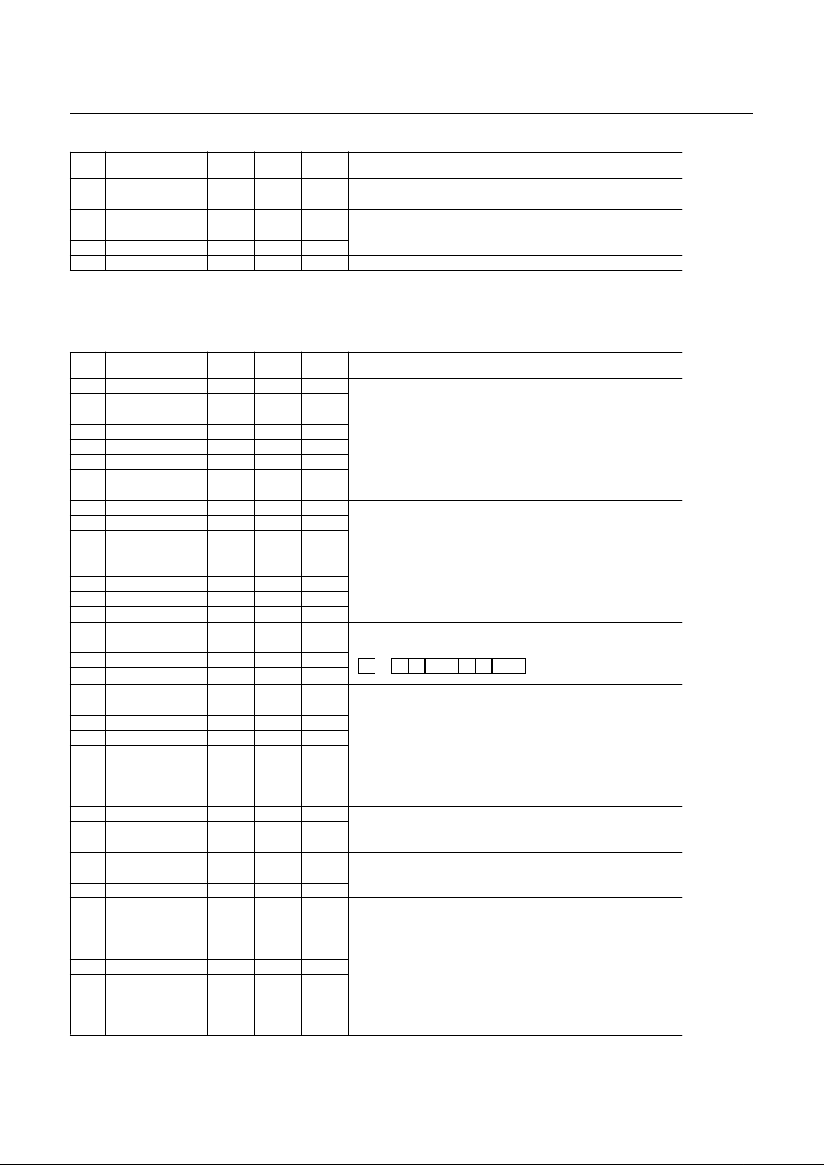
GMS81C4040/87C4060
PRELIMINARY
94
PRELIMINARY
Nov. 1999 Ver 1.0
24.3 Instruction Table by Function
1. Arithmetic/Logic Operation
197 XCN CE 1 5 Exchange nibbles within the accumulator:
N - - - - - Z -
A
7
~ A
4
f
A
3
~ A
0
198 XMA dp BC 2 5
Exchange memory contents with accumulator
N - - - - - Z -199 XMA dp + X AD 2 6 (M)
f
A
200 XMA {X} BB 1 5
201 XYX FE 1 4 Exchange X-register contents with Y-register : X
f
Y - - - - - - - -
NO. MNENONIC
OP
CODE
BYTE
NO.
CYCLE
NO
OPERATION
FLAG
NVGBHIZC
NO. MNENONIC
OP
CODE
BYTE
NO.
CYCLE
NO
OPERATION
FLAG
NVGBHIZC
1 ADC #imm 04 2 2 Add with carry.
NV - - H - ZC
2 ADC dp 05 2 3
A
←
A + (M) + C
3 ADC dp + X 06 2 4
4 ADC !abs 07 3 4
5 ADC !abs+Y 15 3 5
6 ADC [dp+X] 16 2 6
7 ADC [dp]+Y 17 2 6
8 ADC {X} 14 1 3
9 AND #imm 84 2 2 Logical AND
N - - - - - Z -
10 AND dp 85 2 3
A
←
A ^ (M)
11 AND dp + X 86 2 4
12 AND !abs 87 3 4
13 AND !abs+Y 95 3 5
14 AND [dp+X] 96 2 6
15 AND [dp] + Y 97 2 6
16 AND {X} 94 1 3
17 ASL A 08 1 2 Arithmetic shift left
N - - - - - ZC
18 ASL dp 09 2 4
19 ASL dp + X 19 2 5
20 ASL !abs 18 3 5
21 CMP #imm 44 2 2 Compare accumulator contents with memory contents
N - - - - - ZC
22 CMP dp 45 2 3 A - (M)
23 CMP dp + X 46 2 4
24 CMP !abs 47 3 4
25 CMP !abs + Y 55 3 5
26 CMP [dp + X] 56 2 6
27 CMP [dp] + Y 57 2 6
28 CMP {X} 54 1 3
29 CMPX #imm 5E 2 2 Compare X contents with memory contents
N - - - - - ZC30 CMPX dp 6C 2 3 X - (M)
31 CMPX !abs 7C 3 4
32 CMPY #imm 7E 2 2 Compare Y contents with memory contents
N - - - - - ZC33 CMPY dp 8C 2 3 Y - (M)
34 CMPY !abs 9C 3 4
35 COM dp 2C 2 4 1’s complement : (dp)
←
~(dp) N - - - - - Z 36 DAA DF 1 3 Decimal adjust for addition N - - - - - ZC
37 DAS CF 1 3 Decimal adjust for substraction N - - - - - ZC
38 DEC A A8 1 2 Decrement
N - - - - - Z -
39 DEC dp A9 2 4 M
←
M - 1
40 DEC dp + X B9 2 5
41 DEC !abs B8 3 5
42 DEC X AF 1 2
43 DEC Y BE 1 2
C 7 6 5 4 3 2 1 0
← ← ← ← ← ← ← ← ← ← "0
"
Page 99
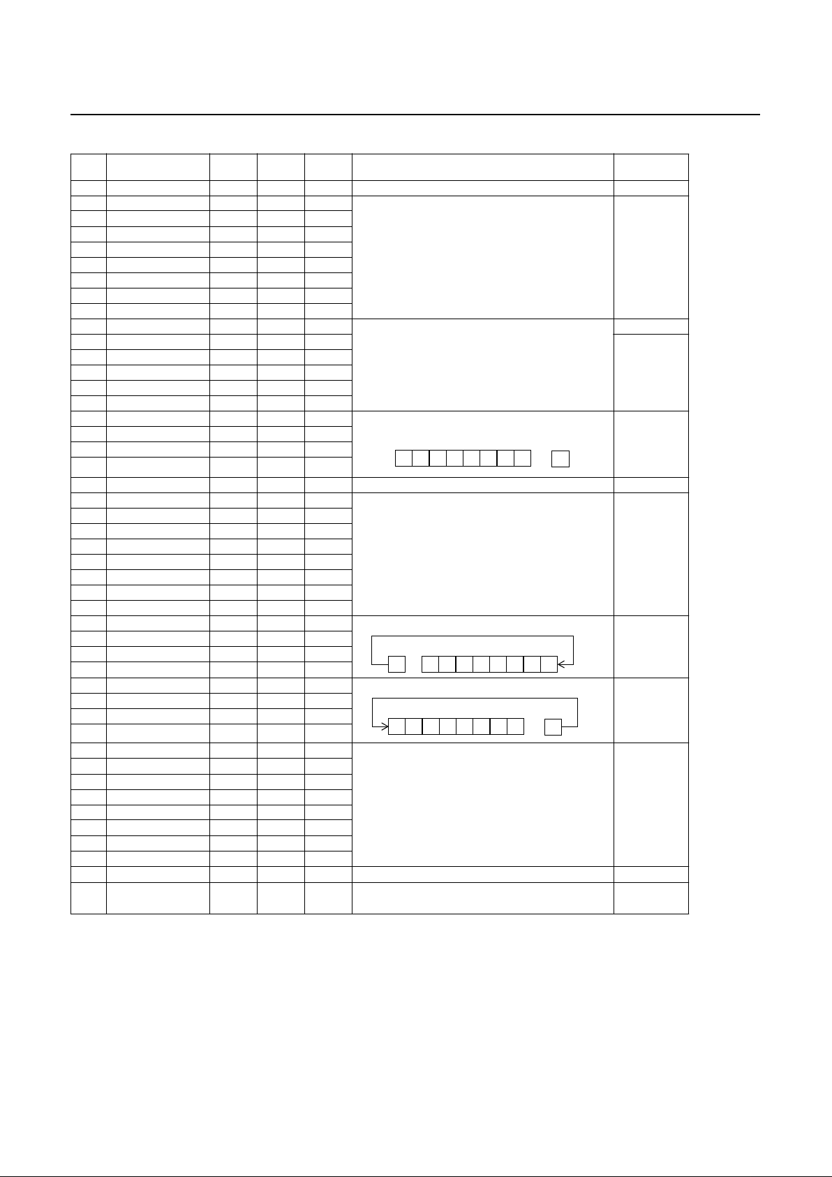
PRELIMINARY
GMS81C4040/87C4060
Nov. 1999 Ver 1.0
PRELIMINARY
95
44 DIV 9B 1 12 Divide : YA/A
←
Q:A, R:Y NV - - H - Z -
45 EOR #imm A4 2 2 Exclusive OR
N - - - - - Z -
46 EOR dp A5 2 3 A
←
A ⊕ (M)
47 EOR dp + X A6 2 4
48 EOR !abs A7 3 4
49 EOR !abs + Y B5 3 5
50 EOR [ dp + X] 96 2 6
51 EOR [dp] + Y 97 2 6
52 EOR {X} 94 1 3
53 INC A 88 1 2 Increment N - - - - - ZC
54 INC dp 89 2 4 (M)
←
(M) + 1
N - - - - - Z -
55 INC dp + X 99 2 5
56 INC !abs 98 3 5
57 INC X 8F 1 2
58 INC Y 9E 1 2
59 LSR A 48 1 2 Logical shift right
N - - - - - ZC
60 LSR dp 49 2 4
61 LSR dp + X 59 2 5
62 LSR !abs 58 3 5
63 MUL 5B 1 9 Multiply : YA
←
Y x A N - - - - - Z -
64 OR #imm 64 2 2 Logical OR
N - - - - - Z -
65 OR dp 65 2 3 A
←
A V (M)
66 OR dp + X 66 2 4
67 OR !abs 67 3 4
68 OR !abs + Y 75 3 5
69 OR [dp +X} 76 2 6
70 OR [dp] + Y 77 2 6
71 OR {X} 74 1 3
72 ROL A 28 1 2 Rotate left through carry
N - - - - - ZC
73 ROL dp 29 2 4
74 ROL dp + X 39 2 5
75 ROL !abs 38 3 5
76 ROR A 68 1 2 Rotate right through carry
N - - - - - ZC
77 ROR dp 69 2 4
78 ROR dp + X 79 2 5
79 ROR !abs 78 3 5
80 SBC #imm 24 2 2 Substract with carry
NV - - HZC
81 SBC dp 25 2 3 A ← A - (M) - ~(C)
82 SBC dp + X 26 2 4
83 SBC !abs 27 3 4
84 SBC !abs + Y 35 3 5
85 SBC [dp + X] 36 2 6
86 SBC [dp] + Y 37 2 6
87 SBC {X} 34 1 3
88 TST dp 4C 2 3
Test memory contents for negative or zero : (dp) - 00
H
N - - - - - Z -
89 XCN CE 1 5 Exchange nibbles within the accumulator:
N - - - - - Z -
A
7
~ A
4
f
A
3
~ A
0
NO. MNENONIC
OP
CODE
BYTE
NO.
CYCLE
NO
OPERATION
FLAG
NVGBHIZC
7 6 5 4 3 2 1 0 C
"0"
→ → → → → → → → → →
C 7 6 5 4 3 2 1 0
← ← ← ← ← ← ← ← ←
7 6 5 4 3 2 1 0 C
→ → → → → → → → →
Page 100
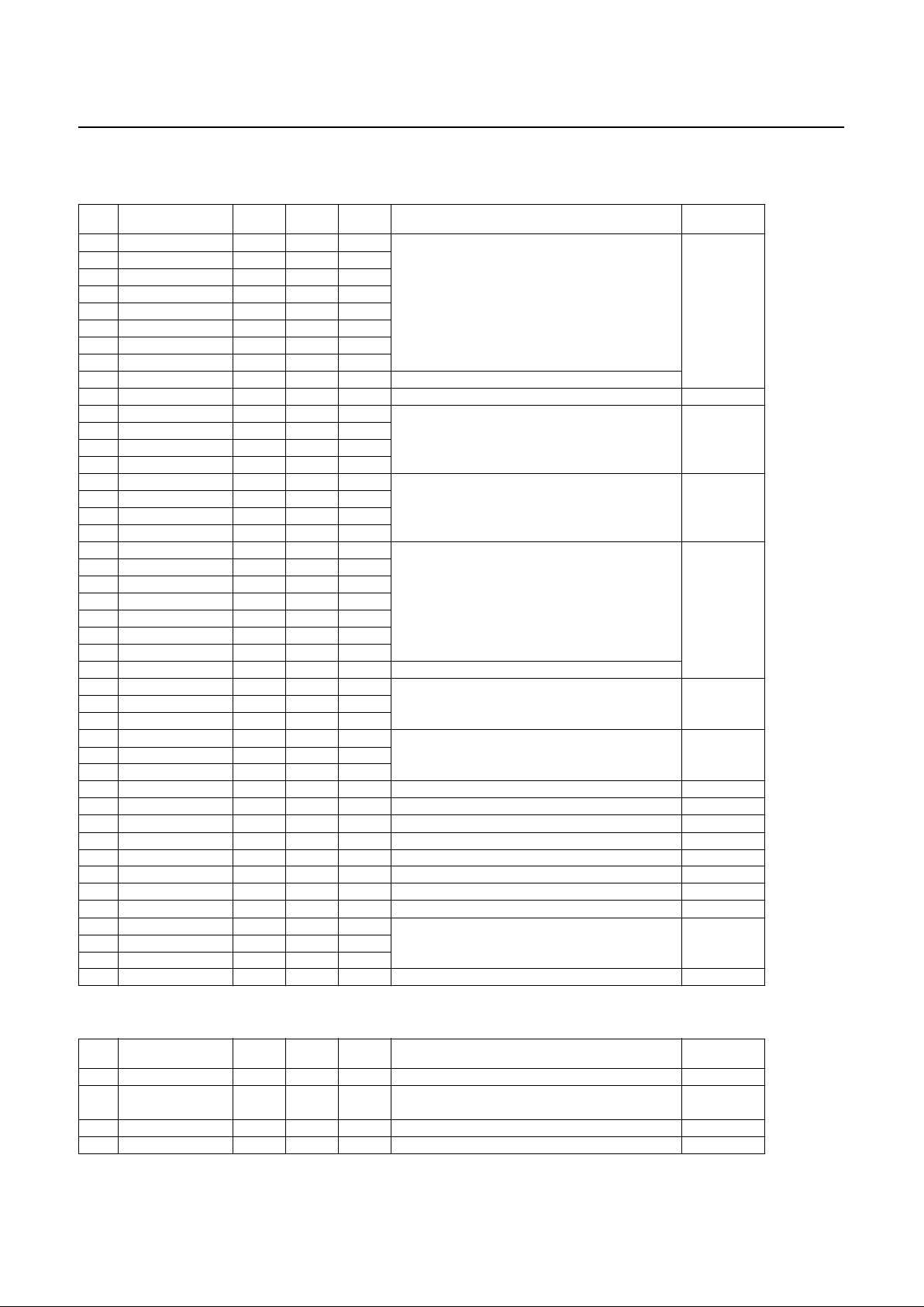
GMS81C4040/87C4060
PRELIMINARY
96
PRELIMINARY
Nov. 1999 Ver 1.0
2. Register / Memory Operation
3. 16-Bit Operation
NO. MNENONIC
OP
CODE
BYTE
NO.
CYCLE
NO
OPERATION
FLAG
NVGBHIZC
1 LDA #imm C4 2 2 Load accumulator
N - - - - - Z -
2 LDA dp C5 2 3 A
←
(M)
3 LDA dp + X C6 2 4
4 LDA !abs C7 3 4
5 LDA !abs + Y D5 3 5
6 LDA [dp + X] D6 2 6
7 LDA [dp]+Y D7 2 6
8 LDA {X} D4 1 3
9 LDA {X}+ DB 1 4 X-register auto-increment : A
←
(M), X ← X + 1
10 LDM dp,#imm E4 3 5 Load memory with immediate data : (M)
←
imm - - - - - - - -
11 LDX #imm 1E 2 2 Load X-register
N - - - - - Z -
12 LDX dp CC 2 3 X
←
(M)
13 LDX dp + Y CD 2 4
14 LDX !abs DC 3 4
15 LDY #imm 3E 2 2 Load X-register
N - - - - - Z -
16 LDY dp C9 2 3 Y
←
(M)
17 LDY dp + Y D9 2 4
18 LDY !abs D8 3 4
19 STA dp E5 2 3 Store accumulator contents in memory
- - - - - - - -
20 STA dp + X E6 2 4 (M) ← A
21 STA !abs E7 3 4
22 STA !abs + Y F5 3 5
23 STA [dp + X] F 6 2 6
24 STA [dp] + Y F7 2 6
25 STA {X } F4 1 3
26 STA {X}+ FB 1 4 X-register auto-increment : (M) ← A, X ← X + 1
27 STX dp EC 2 4 Store X-register contents in memory
- - - - - - - -28 STX dp + Y ED 2 5 (M) ← X
29 STX !abs FC 3 5
30 STY dp E9 2 4 Store Y-register contents in memory
- - - - - - - -31 STY dp + X F9 2 5 (M) ← Y
32 STY !abs F8 3 5
33 TAX E8 1 2 Transfer accumulator contents to X-register : X ← A N - - - - - Z 34 TAY 9F 1 2 Transfer accumulator contents to Y-register : Y ← A N - - - - - Z 35 TSPX AE 1 2
Transfer stack-pointer contents to X-register : X
← SP N - - - - - Z 36 TXA C8 1 2 Transfer X-register contents to accumulator : A ← X N - - - - - Z 37 TXSP 8E 1 2 Transfer X-register contents to stack-pointer : SP ← X N - - - - - Z 38 TYA BF 1 2 Transfer Y-register contents to accumulator : A ← Y N - - - - - Z 39 XAX EE 1 4 Exchange X-register contents with accumulator : X fA - - - - - - - 40 XAY DE 1 4 Exchange Y-register contents with accumulator : Y fA - - - - - - - 41 XMA dp BC 2 5
Exchange memory contents with accumulator
N - - - - - Z -42 XMA dp + X AD 2 6 (M)
f
A
43 XMA {X} BB 1 5
44 XYX FE 1 4 Exchange X-register contents with Y-register : X
f
Y - - - - - - - -
NO. MNENONIC
OP
CODE
BYTE
NO.
CYCLE
NO
OPERATION
FLAG
NVGBHIZC
1 ADDW dp 1D 2 5 16-bits add without carry : YA
←
YA + (dp+1)(d p) NV - - H - ZC
2 CMPW dp 5D 2 4 Compare YA contents with memory pair contents : N - - - - - ZC
YA - (dp+1)(dp)
3 DECW dp BD 2 6 Decrement memory pair : (dp+1)(dp)
←
{(dp+1)(dp)} - 1 N - - - - - Z -
4 INCW dp 9D 2 6 Increment memory pair : (dp+1)(dp)
←
{(dp+1)(dp)} + 1 N - - - - - Z -
 Loading...