

Page 1

Rev. 2.1NOV. 1996
USER’S MANUAL
HYUNDAI MicroElectronics
GMS84512 / 84524
8-BIT SINGLE CHIP MICROCOMPUTER
Page 2

GMS84512/84524 USER’ S MANUAL
Table of Contents
1. Overview
2. CPU
3. Peripheral Function
4. Control Function
5. Support Tool
6. Appendix
Page 3

1. Overview
1. Features
2. Block Diagram
3. Summary Of Peripheral Function Register
4. Pin Assignment
5. Pin Description
6. Terminal Types
2. CPU
1. Registers
2. Memory Space
3. Peripheral Function
1. PORT
2. Clock Generation Circuit
3. Timer
4. A/D Comparator
5. Serial I/O
6. PWM
7. Interrupt Interval Measurement Circuit
8. On Screen Display
4. Control Function
1. Interrupts
2. Standby Function
3. Reset Function
5. Support Tool
1. Emulator
2. Debugger
3. Assembler
4. Linker
5. Font Editor
6. OTP Chip
6. Appendix
l Electrical Data
l Package Outline
Page 4

GMS 84512 / 84524
1 - 1
An 8-bit microcomputer using the G8MC Core is a single-chip microcomputer including several peripheral
functions such as Timer, I/O Comparator, Serial I/O, PWM, Watch-dog Timer and On-Screen Display.
1.1 FEATURES
l ROM 12,288 Bytes ( GMS84512 ) 24,576Bytes ( GMS84524 )
l RAM 256 Bytes
l Minimum instruction execution time1 us ( @ Xin = 4 MHz )
l I/O PORT 42 ( INPUT: 3, OUTPUT: 10, I/O: 29 )
l Serial I/O 8-bit X1 ch. ( 1MHz, 500KHz, 250 KHz, Ext. clock )
l A/D Comparator 5-bit X4 ch. ( max. 1 LSB )
l Pulse Width Modulation 14-bit X1 ch.
7-bit X8 ch.
l Timer
- Timer/Counter 8 bit X4 ch. ( 16-bit X2 ch is Acceptable)
- Basic Interval Timer 8 bit X1 ch.
- Watch Dog Timer
l Interrupt Interval estimation circuit for Remocon signal receiving
l Interrupt Sources 14 sources
l Pulse ( T2048 ) Output Function Period : 2,048 us, Duty: 50 %
l On Screen Display
- Kinds of character 128 kinds (include 2 test characters)
- Construction of character 14 dots X18 dots
- Size of character 4 X4 kinds
- Number of display character 22 Characters X3 lines ( Max. 12 lines)
- Display colors 8 kinds
- Color Edge, Smoothing Function
l Power Save Mode STOP mode
l Operating Voltage 4.5 ~5.5 V
l Package 52 SDIP
l
OTP chip GMS84512T/84524T
Page 5
GMS 84512 / 84524
1 - 2
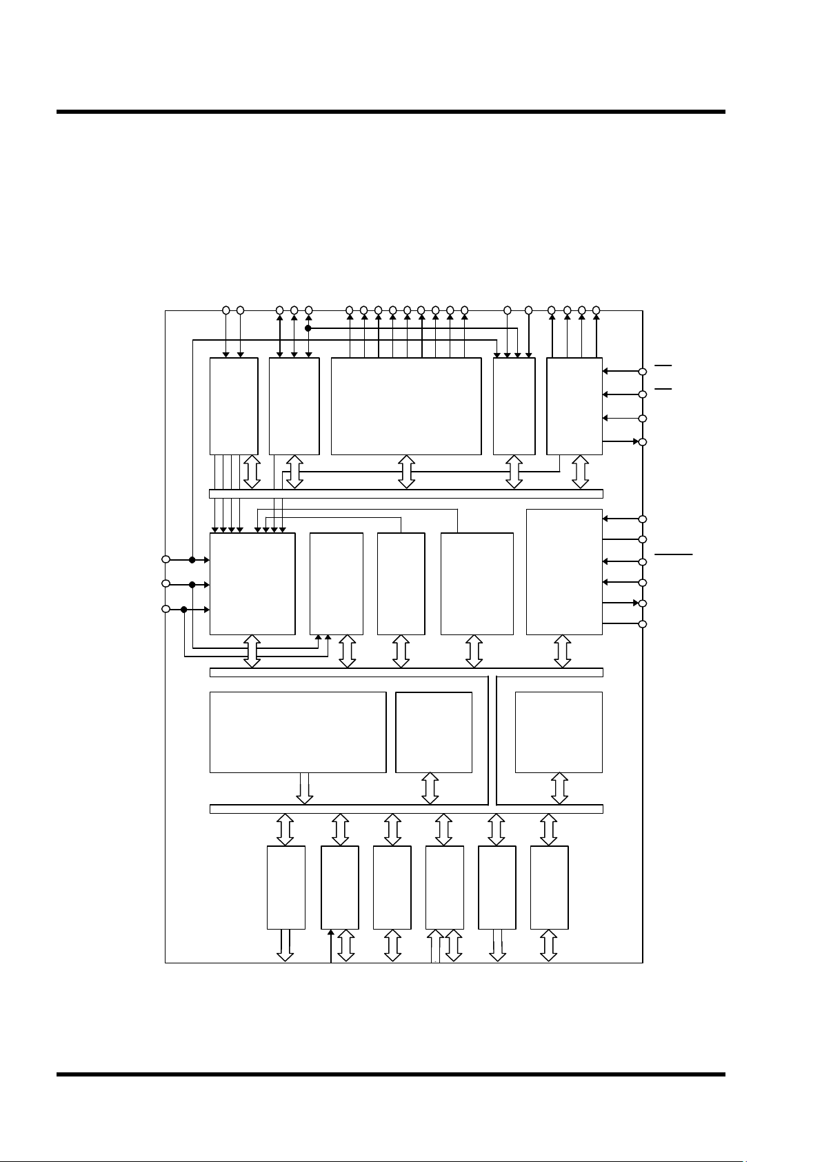
1.2 BLOCK DIAGRAM
R40 ~ R45
G8MC
CORE
R20 ~ R27
R2 PORT
R32 ~ R37
R3 PORT
R00 ~ R07
R0 PORT
R10 ~ R16
R1 PORT
R50 ~ R53
R5 PORT
PWM
A/D COMP.
R53/ Y
R52/ B
R50/ R
R51/ G
R15/ Cin1
R16/ Cin2
R43/ PWM2
R42/ PWM3
R45/ PWM0
R44/ PWM1
R37/ PWM6
R36/ PWM7
R41/ PWM4
R40/ PWM5
R32/ PWM8
R26/ EC2
R27/ EC3
R33/ Sout
R35/ Sin/ Cin3
R34/ Sclk
INTERRUPT
CONTROLLER
REMOCON
TIMER
SERIAL
I/O
CLOCK GEN./
SYSTEM CON.
OSD
R30/ INT1
R31/ INT2
HD
VD
R17/ Cin0/ INT3
OSC2
OSC1
Vdd
TEST
Xin
RESET
Vss
Xout
RAM
( 256 byte )
WATCH DOG
TIMER
R30 ~ R31
R17
R4 PORT
ROM
( 12K / 24K)
PRESCALER
/ B.I.T.
Page 6

GMS 84512 / 84524
1 - 3
1.2 Peripheral Function Overview
BLOCK
Function
INDEX
PRESCALER
/ B.I.T.
Prescaler is consists of 10 bits binary counter, and divide oscillation clock.
The divided output from each bit of prescaler provided to peripheral hardware.
B.I.T a 8 bit binary counter has a function such as security of oscillation
stabilization time, generation of basic interval time interrupt as watch function,
providing the clock for watch-dog timer
3 - 13
WATCH-DOG
-TIMER
WDT is consist of 6-bit binary counter, WDTR(Watch-Dog Timer Register), and
comparator, input clock of WDT is provided by Basic Interval Timer interrupt
and maximum output cycle is 4 seconds.
When WDTOM is ‘1’, the output of WDT reset the Device.
3 -16
TIMER /
COUNTER
Timer is an 8 bit binary counter and consisted of T0, T1, T2, T3.
As an 8-bit binary counter, each T0, T1 can be used 16-bit interval Timer to
connect each other. As an 8 bit binary counter/event counter each T2, T3 can
be used 16-bit/event counter to connect each other.
At 4 MHz oscillation, Maximum interval time of T0 is 8.192 ms, T1 is 2048 ms,
T0-T1 is about 2 seconds, T2 is 2.048 ms, T3 is 512uS,T2-T3 is about 0.5
seconds
3 - 19
A/D COMP ARATOR
A/D Comparator has 5 bit resolution, and 4 input channel. It has sample and
hold function of input. At 4 MHz it takes about 8uS to compare. Error is less
than 1/2 LSB.
3 - 26
SERIAL I/O
It is 8 bit clock synchronous serial interface unit, the clock transmission cycle is
1uS,2uS,4uS Which can be selected external clock. When IOSW(Bit 6 Of
Serial I/O Mode Register) is ‘1’, R33 pin operates Sout at transmission mode,
Sin at receiving mode.
3 - 28
PWM
( Pulse Width
Modulation )
PWM is consists of 14 bit PWM 1 ch and 7 bit PWM 8 ch.
14 bit PWM has 0.5uS minimum resolution width, 8192uS cycle time, 7 bit
PWM has 8uS minimum resolution 8uS,1024uS, cycle time. The polarity of
PWM output can be assign by Software.
3 - 32
INTERRUPT
INTERVAL
MEASUREMENT CIRCUIT
Interrupt interval measurement circuit consists of 8 bit binary counter, interrupt
interval saving circuit. It can select 32uS, 64uS as a measurement clock .
Because it can select external signal edge, measurement of input signal cycle
or pulse width is possible. So it can be used Remocon receiving.
3 - 38
OSD
( On-Screen Display )
Maximum number of character or symbol displayed in CRT is 128 basically
displayed by 22 charactersX3 lines. Maximum 12 lines is possible with OSD
interrupt.
OSD clock can use 4 MHz ~ 8 MHz size of display character is 16 kinds, it can
be used by line unit. The color of display character is 8 kinds it can be used by
character unit. In display mode, there are character mode, background mode,
color mode, and Blanking mode, it can be used by line unit especially
smoothing function and OSD oscillator control function exists.
3 - 41
Page 7
GMS 84512 / 84524
1 - 4
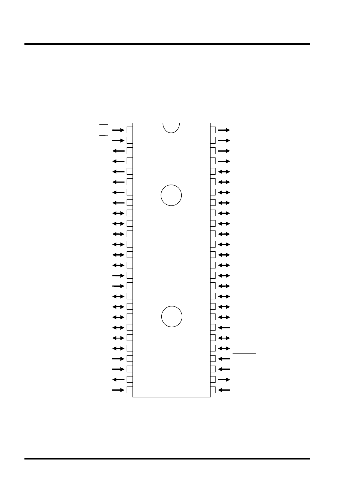
1.4 PIN ASSIGNMENT
1
HD
52
R50/ R
2
VD
51
R51/ G
3
R45/ PWM0
50
R52/ B
4
R44/ PWM1
49
R53/ Y
5
R43/ PWM2
48
R00
6
R42/ PWM3
47
R01
7
R41/ PWM4
46
R02
8
R40/ PWM5
45
R03
9
R37/ PWM6
44
R04
10
R36/ PWM7
43
R05
11
R35/ Sin/ Cin3
42
R06
12
R34/ Sclk
41
R07
13
R33/ Sout
40
R10
14
R32/ PWM8
39
R11
15
R31/ INT2
38
R12
16
R30/ INT1
37
R13
17
R27/ EC3
36
R14
18
R26/ EC2
35
R15/ Cin1
19
R25/ T2048
34
R16/ Cin2
20
R24
33
R17/ Cin0/ INT3
21
R23
32
R20
22
R22
31
R21
23
TEST
30
RESET
24
Xin
29
OSC1
25
Xout
28
OSC2
26
Vss
27
Vdd
HME
GMS84512/84524
Page 8
GMS 84512 / 84524
1 - 5
1.5 PIN DESCRIPTION
Classification No.
Symbol
I/O Function Type Remark
Power
27 Vdd Input Power supply (4.5~5.5V)
26 Vss Input Ground (0V)
System
23 TEST Input TEST Input pin
Control or
At 'L' input: SINGLE CHIP MODE
IA
Clock
At 'H' input : TEST MODE
24 Xin Input CRYSTAL connection pin (with Xout)
If an external clock is used, Xin pin should be
connected external clock source
25 Xout Output CRYSTAL connection pin(with Xin)
If an external clock used, Xout pin
should be open
30 RESET Input In the state of 'L' level, system
IA
enter the reset state
OSD
1 HD Input Horizontal synchronizing signal input pin
IA
2 VD Input Vertical synchronizing signal input pin
28 OSC2 Ouptut Clock output for OSD
29 OSC1 Input Clock input for OSD
49 Y Output Switching signal output pin R53 share
50 B Output BLUE signal output pin
OA
R52 share
51 G Output GREEN signal output pin R51 share
52 R Output RED signal output pin R50 share
PWM
3 PWM0 Output Pulse width modulation output pin R45 share
4 PWM1 Output (7BIT PWM) R44 share
5 PWM2 Output
OB
R43 share
6 PWM3 Output R42 share
7 PWM4 Output R41 share
8 PWM5 Output R40 share
9 PWM6 Output
IOF
R37 share
10 PWM7 Output R36 share
14 PWM8 Output 14BIT PWM output pin
IOD
R32 share
19 T2048 Output Pulse(2048uS) output pin R25 share
SCI
11 Sin Input Serial Data Input pin
IOE
R35 share
12 Sclk I/O Serial Clock I/O pin
IOG
R34 share
13 Sout Output Serial Data output pin R33 share
TIMER
17 EC3 Input Event Counter input pin
IOB
R27 share
Page 9
GMS 84512 / 84524
1 - 6
Classification NO.
Symbol
I/O Function
TYPE
Remarks
Interrupt
15 INT2 Input External interrupt request input pin
IB
R31 share
16 INT1 Input (INT1,INT2 : Remocon input capture R30 share
33 INT3 Input Input possible)
IC
R17 share
A/D
11 Cin3 Input Analog input pin
IOE
R35 share
Comparator
33 Cin0 Input (Default selection : Cin0)
IC
R17 share
34 Cin2 Input
IOC
R16 share
35 Cin1 Input R15 share
I/O Port
41 R07 I/O R0 Port
~
~
(Can assigned I/O state bit by bit by R0DD)
IOA
48 R00 I/O
33 R17 Input R1 Port ( R17 Input only )
IC
Cin0/INT3 share
34 R16 I/O ( 7 ports of R10~R16 can assigned I/O
IOC
Cin2 shrae
~
~
state bit by bit by R1DD Cin1 share
40 R10 I/O
IOA
17 R27 I/O R2 Port
IOB
EC3 share
18 R26 I/O ( Can assigned I/O state bit by bit EC2 share
19 R25 I/O by R2DD)
IOD
T2048 share
20 R24 I/O
21 R23 I/O
22 R22 I/O
IOA
31 R21 I/O
32 R20 I/O
9 R37 I/O R3 PORT
IOB
PWM6 share
10 R36 I/O ( 6 Bits of R31~R32 can assigned I/O PWM7 share
11 R35 I/O state bit by bit by R3DD
IOE
Sin/Cin3 share
12 R34 I/O
IOG
Sclk share
13 R33 I/O Sout share
14 R32 I/O
IOD
PWM8 share
15 R31 Input ( R30,R31 is input only)
IB
INT2 share
16 R30 Input INT1 share
3 R45 Output R4 Port PWM0 share
4 R44 Output ( 6 bit output only ) PWM1 share
5 R43 Output
OB
PWM2 share
6 R42 Output PWM3 share
7 R41 Output PWM4 share
8 R40 Output PWM5 share
49 R53 Output R5 Port Y share
50 R52 Output ( 4 bit output only )
OA
B share
51 R51 Output G share
52 R50 Output R share
Page 10
GMS 84512 / 84524
1 - 7
1.6 TERMINAL TYPES
PIN TERMINAL TYPE at RESET
Xin
Xout
Oscillation
OSC1
OSC2
Oscillation
Stop
RESET
HD
VD
TEST
( “L” )
Hi-Z
R30/ INT1
R31/ INT2 Hi-Z
R17/ Cin0
/ INT3 Hi-Z
IA type
IB type
INT1,INT2
Data Bus
I
Vdd
Vss
Rd
SCHMITT Input
IC type
INT1,INT2
Data Bus
I
Vdd
Vss
Rd
SCHMITT Input
Cin3
Test Pin is using normal
gate
SCHMITT Input
RST
H Sync
V sync
I
Vdd
Vss
Vss
Xin
Xout
Vdd
Vdd
Vss
Vdd
Vss
OSDON
Vss
Vss
Xin
Xout
Vdd
Vss
Vdd
Vss
Vdd
Vss
STOP
Vss
Page 11
GMS 84512 / 84524
1 - 8
PIN TERMINAL TYPE at RESET
R50/ R
R51/ G
R52/ B
R53/ Y
Hi-Z
R45/ PWM0
R44/ PWM1
R43/ PWM2
R42/ PWM3
R41/ PWM4
R40/ PWM5
Hi-Z
R00~R07
R10~R14
R20~R24
Hi-Z
R26/ EC2
R27/ EC3
Hi-Z
OA type
OB type
IOA type
IOB type
Data REG.
Data Bus
PWM0¡-PWM5
Vss
Selection
MUX
O
Vss
Vdd
Vss
Vdd
Vss
Data Bus
R, G, B, Y
Selection
MUX O
Data REG.
Data Bus
Vss
Vdd
Vss
Data Bus
MUX
IO
Direction REG.
Vdd
Data Bus
Data REG.
Rd
EC2, EC3
SCHMITT input
Data Bus
Vss
Vdd
Vss
Data Bus
MUX
IO
Direction REG.
Vdd
Data Bus
Data REG.
Rd
Page 12
GMS 84512 / 84524
1 - 9
PIN TERMINAL TYPE at RESET
R15/ Cin1
R16/ Cin2
Hi-Z
R25/ T2048
R32/ PWM8 Hi-Z
R35/ Sin
/ Cin4
Hi-Z
IOC type
IOD type
IOE type
Cin1, Cin2
Data Bus
Vss
Vdd
Vss
Data Bus
MUX
IO
Direction REG.
Vdd
Data Bus
Data REG.
Rd
Rd
Data Bus
Vss
Vdd
Vss
Data Bus
MUX
MUX
IO
Vdd
Selection
T2048, PWM8
Data Bus
Data REG.
Direction REG.
Sin
Data Bus
Vss
Vdd
Vss
Data Bus
MUX
IO
Vdd
Selection
Data Bus
Data REG.
SCHMITT input
Direction REG.
Rd
Cin4
Page 13
GMS 84512 / 84524
1 - 10
PIN TERMINAL TYPE at RESET
R36/ PWM7
R37/ PWM6
Hi-Z
R34/ Sclk
R33/ Sout
Hi-Z
Data Bus
IOF type
IOG type
MUX
SCHMITT input
Rd
Rd
Data Bus
Vss
Vss
Data Bus
MUX
IO
Selection
PWM6,PWM7
Data Bus
Data REG.
Direction REG.
MUX
Vss
Vss
Data Bus
IO
Selection
PWM6,PWM7
Data Bus
Data REG.
Direction REG.
MUX
Page 14

GMS84512/84524 USER’ S MANUAL
Table of Contents
1. Overview
2. CPU
3. Peripheral Function
4. Control Function
5. Support Tool
6. Appendix
Page 15
GMS 84512 / 84524
2 - 1
2.1. REGISTERS
Program Counter
15 8
PCH
7 0
PCL
A - Register
7 0
A
15 8
Y
( YA 16bit Accumulator )
7 0
A
X - Register
7 0
X
Y - Register
7 0
Y
Program Status Word
7 0
PSW
Stack Pointer *1
7 0
SP
Carry Flag
Z CH IG BN V
Zero Flag
Interrupt Enable Flag
Half Carry Flag
Break Flag
G ( Direct Page ) Flag
Overflow Flag
Negative Flag
15 8
*1 STACK ADDRESS ( 0100H~-013FH )
01
H
Hardware fixed
7 0
SP
Page 16

GMS 84512 / 84524
2 - 2
2.1.1. A - Register
l 8 bit Accumulator
l In the case of 16-bit operation, compose the lower 8-bit of YA (16-bit Accumulator)
l In the case of multiplication instruction, execute as a multiplier register.
After multiplication operation, the lower 8-bit of the result enters. (Y * A → YA)
l In the case of division instruction, execute as the lower 8-bit of dividend.
After division operation, quotient enters. (YA ¡À X ¡æ Q: A , R: Y )
2.1.2. X- Register
l General-purpose 8-bit register
l In the case of index addressing mode within direct page(RAM area), execute as index
register
l In the case of G mode operation, execute as destination address register.
The operation result enters into memory indirectly addressed by X register.
l In the case of division instruction, execute as divisor register.
2.1.3. Y- Register
l General-purpose 8-bit register
l In the case of index addressing mode, execute as index register
l In the case of 16-bit operation instruction, execute as the upper 8-bit of YA (16-bit
accumulator).
l In the case of multiplication instruction, execute as a multiplicand register.
After multiplication operation, the upper 8-bit of the result enters.
l In the case of division instruction, execute as the upper 8-bit of dividend.
After division operation, quotient enters.
l Can be used as loop counter of conditional branch command. (e.g. DBNE Y, REL)
2.1.4. Stack Pointer
l In the cases of subroutine call, Interrupt and PUSH, POP, RETI, RET instruction,
stack data on RAM or in the case of returning, assign the storage location having
stacked data.
l Stack area is constrained within 1-page (00H-FFH). Page is fixed by H/W. User can
only assign the lower address. At the initial stage, stack pointer should be initialized to
Page 17
GMS 84512 / 84524
2 - 3
point to RAM area having H/W.
¨çInterrupt
¨èRETI
¨éSubroutine CALL
¨êRET
¨ëPUSH A ( X, Y, PSW )
¨ìPOP A ( X, Y, PSW )
M (sp) ¡ç ( PCH )
sp ¡ç sp - 1
M (sp) ¡ç PCL )
sp ¡ç sp - 1
M (sp) ¡ç A
M (sp) ¡ç ( PCH )
sp ¡ç sp - 1
M (sp) ¡ç ( PCL )
sp ¡ç sp - 1
M (sp) ¡ç ( PSW )
sp ¡ç sp - 1
sp ¡ç sp - 1
sp ¡ç sp + 1
( PCL ) ¡ç M (sp)
sp ¡ç sp + 1
( PCH) ¡ç M (sp)
sp ¡ç sp + 1
A ¡ç M (sp)
( PSW ) ¡ç M (sp)
sp ¡ç sp + 1
( PCL ) ¡ç M (sp)
sp ¡ç sp + 1
( PCH) ¡ç M (sp)
sp ¡ç sp + 1
Page 18

GMS 84512 / 84524
2 - 4
2.1.5. Program Counter ( PC )
l Program counter is a 16-bit counter consisted of 8-bit register PCH and PCL.
l Addressing space is 64K bytes.
l In reset state, Reset routine address in address FFFFH and FFFEH enter into PC.
2.1.6. Program Status Word( PSW )
l PSW is an 8-bit register.
l Consisted of the flags to show the post state of operation and the flags determining
the CPU operation, initialized as 00H in reset state.
PSW
¨çCarry Flag ( C )
l After operation, set when there is a carry from bit7 of ALU or there is not a borrow.
l Set by SETC and clear by CLRC.
l Executable as 1-bit accumulator.
l Branch condition flag of BCS, BCC.
¨èZero Flag ( Z )
l After operation also including 16-bit operation, set if the result is “0”.
l Branch condition flag of BEQ, BNE.
¨éInterrupt Enable Flag ( I )
l Master enable flag of interrupt except for RST(reset).
l Set and cleared by EI, DI .
¨êHalf Carry Flag ( H )
l After operation, set when there is a carry from bit3 of ALU or there is not a borrow
from bit4 of ALU.
l Can not be set by any instruction.
l Cleared by CLRV instruction like V flag.
7
N6V5G4B3H
2
I
1
Z0C
Page 19
GMS 84512 / 84524
2 - 5
¨ëBreak Flag ( B )
l Set by BRK (S/W interrupt) instruction to distinguish BRK and TCALL instruction
having the same vector address.
¨ìDirect Page Flag ( G )
l Assign direct page (0-page, 1-page).
l Set and cleared by SETG, CLRG instruction.
l If used with PG2R(00FC
H
) it is enable to access 2-page ( OSD RAM ).
G-flag PG2R Direct Page
0 -
0 - Page Access
1 0
1 - Page Access
1
2 - Page Access
*NOTICE : Always after clearing, PG2R is enable to be accessed for it is the register
of 0-page
¨íOverflow Flag ( V )
l After operation, set when overflow or underflow occurs.
l In the case of BIT instruction, bit6 of memory location is input to V-flag.
l Cleared by CLRV instruction, but not set by any instruction.
l Branch condition flag of BVS, BVC.
¨îNegative Flag ( N )
l N-flag is set whenever the result of a data transfer or operation is negative (bit7 isset to “1”).
l In the case of BIT instruction, bit7 of memory location is inputted to N-flag
l No CLEAR and SET instruction.
l Branch condition flag of BPL, BMI.
Page 20

GMS 84512 / 84524
2 - 6
2.2 MEMORY SPACE
The memory space of GMS84512/84524 is 64K byte, it is equipped with RAM area, OSD RAM
area, FONT ROM area and PROGRAM ROM area.
2.2.1. RAM area
0-PAGE ( 0000
H
- ~ 00FFH )
RAM 192 Bytes ( 0000
H
~ 00BFH ) and peripheral function register( 00C0H ~ 00FFH )
1-PAGE ( 0100
H
~ 013FH )
RAM 64 Bytes ( 0100
H
~ 013FH ) and STACK area
2-PAGE ( 0200
H
~ 02D5H )
OSD RAM 182 Bytes ( 0200
H
~ 02D5H )
2.2.2. FONT ROM area ( 2000
H
~
3FFFH )
128 character OSD FONT
2.2.3. PROGRAM ROM area
Approximately ROM memory is 12 K bytes and it is domain of User Program.
The highest page(FF00
H
~ FFFFH ) is called U- Page and it is utilized domain as following.
PCALL area ( FF00
H
~ FFBFH )
Domain of jumping at PCALL instruction
TCALL Vector area ( FFC0
H
~ FFDFH )
Storage domain of vector address at TCALL instruction.
Interrupt Vector area ( FFE0
H
~ FFFFH )
Storage domin of interrupt vector address,inclusive RESET
Page 21
GMS 84512 / 84524
2 - 7
MEMORY MAP (GMS84512/84524 )
FFFF
H
FFE0
H
FFC0
H
PROGRAM ROM
No H/W
No H/W
INTERRUPT VECTOR AREA
TCALL VECTOR AREA
PCALL AREA
FONT ROM
( 8 K bytes )
OSD RAM
( 182 Bytes )
No H/W
RAM ( STACK ) ( 64 Bytes )
PERIPHERAL REGISTERS
RAM
( 192 Bytes )
FF00
H
A000
H
D000
H
3FFF
H
2000
H
02D5
H
0200
H
013F
H
0100
H
00FF
H
00BF
H
0000
H
0-PAGE
1-PAGE
2-PAGE
DIRECT-PAGE
GMS84524
( 24K Bytes )
GMS84512
( 12K Bytes )
U-PAGE
Page 22
GMS 84512 / 84524
2 - 8
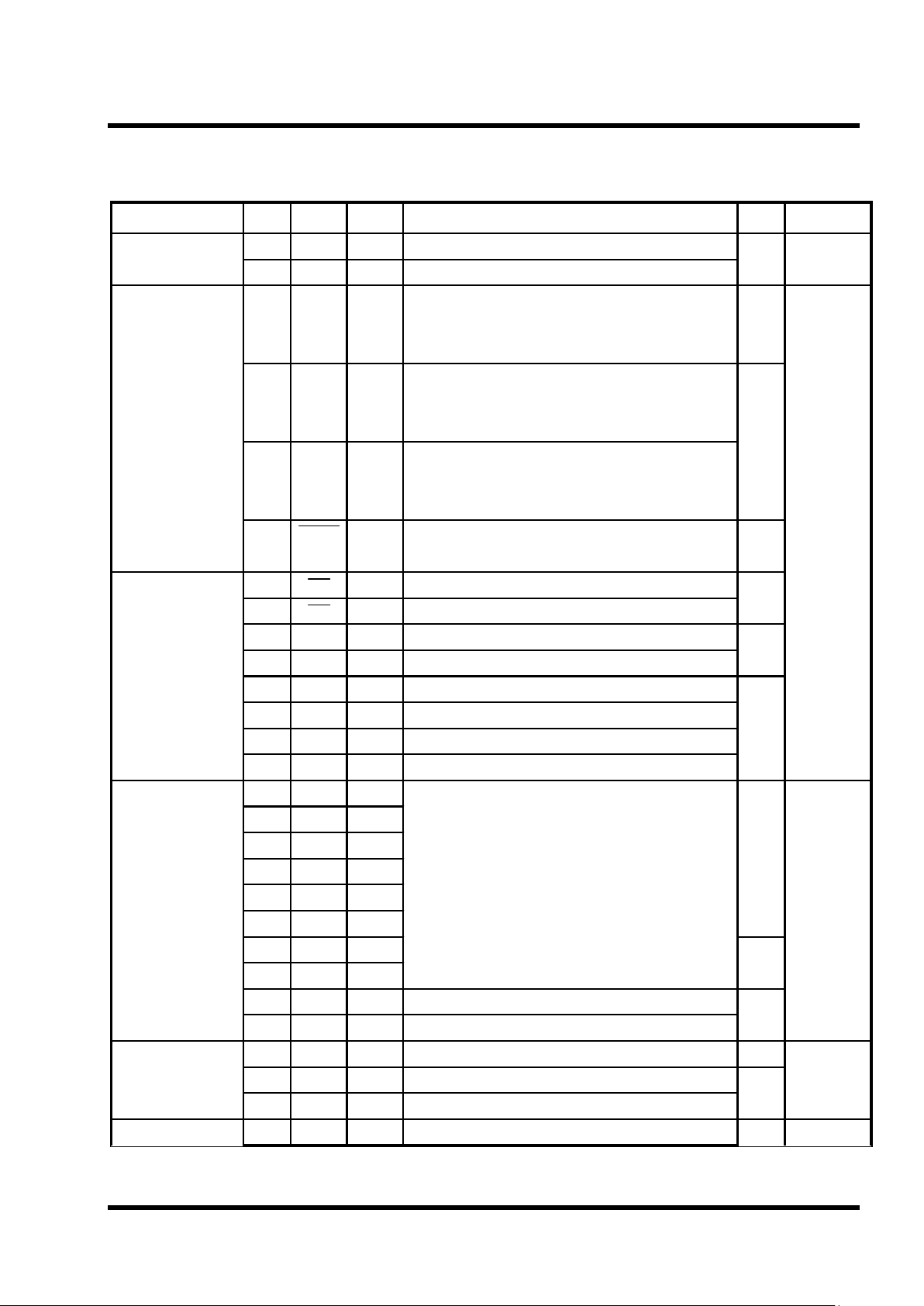
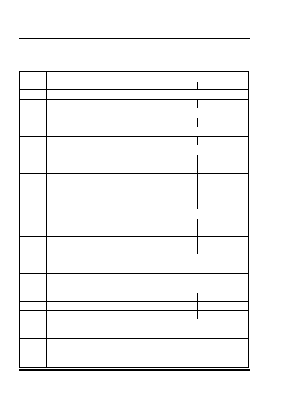
TABLE 2.1. PERIPHERALREGISTER LIST
Address Register Name SYMBOL R/W
RESET VALUE
Page
7 6 5 4 3 2 1 0
00C0
H
R0 PORT DATA REGISTER R0 R/W
Undefined
3 - 1
00C1
H
R0 PORT I/O DIRECTION REGISTER R0DD W 0 0 0 0 0 0 0 0 3 - 1
00C2
H
R1 PORT DATA REGISTER R1 R/W
Undefined
3 - 2
00C3
H
R1 PORT I/O DIRECTION REGISTER R1DD W - 0 0 0 0 0 0 0 3 - 2
00C4
H
R2 PORT DATA REGISTER R2 R/W
Undefined
3 - 4
00C5
H
R2 PORT I/O DIRECTION REGISTER R2DD W 0 0 0 0 0 0 0 0 3 - 4
00C6
H
R3 PORT DATA REGISTER R3 R/W
Undefined
3 - 6
00C7
H
R3 PORT I/O DIRECTION REGISTER R3DD W 0 0 0 0 0 0 - - 3 - 6
00C8
H
R4 PORT DATA REGISTER R4 R/W - -
Undefined
3 - 9
00C9
H
R5 PORT DATA REGISTER R5 R/W - - - - Undefined 3 - 10
00CA
H
PORT FUNCTION SELECTION REGISTER FUNC W - - - 0 0 0 0 0 3 - 3
00CB
H
EXT. INTERRUPT EDGE SELECTION REGISTER IEDS W - - 0 0 0 0 0 0 3 - 39
00CC
H
OPERATION MODE REGISTER TMR W - - - - - 0 0 0
¡ª
00CE
H
BASIC INTERVAL TIMER REGISTER BITR R
Undefined
3 - 16
CLOCK CONTROL REGISTER CKCTLR W - - 0 1 0 1 1 1 3 - 13
00CF
H
WATCH-DOG TIMER REGISTER WDTR W - 0 1 1 1 1 1 1 3 - 17
00D0
H
TIMER MODE REGISTER0 TM0 R/W - 0 0 0 0 0 0 0 3 - 21
00D1
H
TIMER MODE REGISTER2 TM2 R/W - 0 0 0 0 0 0 0 3 - 21
00D2
H
TIMER0 DATA REGISTER TDR0 R/W
Undefined
3 - 21
00D3
H
TIMER1 DATA REGISTER TDR1 R/W
Undefined
3 - 21
00D4
H
TIMER2 DATA REGISTER TDR2 R/W
Undefined
3 - 21
00D5
H
TIMER3 DATA REGISTER TDR3 R/W
Undefined
3 - 21
00D6
H
A/D COMPARATOR MODE REGISTER CMR W *6 0 0 - 0 0 0 0 0 3 - 27
00D7
H
A/D COMP. CHANNEL SELECTION REGISTER CIS W - - - - - - 0 0 3 - 27
00D8
H
SERIAL I/O MODE REGISTER SIOM R/W *0 - 0 0 0 0 0 0 1 3 - 29
00D9
H
SERIAL I/O DATA REGISTER SIOR R/W
Undefined
3 - 28
00DA
H
PWM0 DATA REGISTER PWMR0 W -
Undefined
3 - 35
00DB
H
PWM1 DATA REGISTER PWMR1 W -
Undefined
3 - 35
00DC
H
PWM2 DATA REGISTER PWMR2 W -
Undefined
3 - 35
00DD
H
PWM3 DATA REGISTER PWMR3 W -
Undefined
3 - 35
Page 23
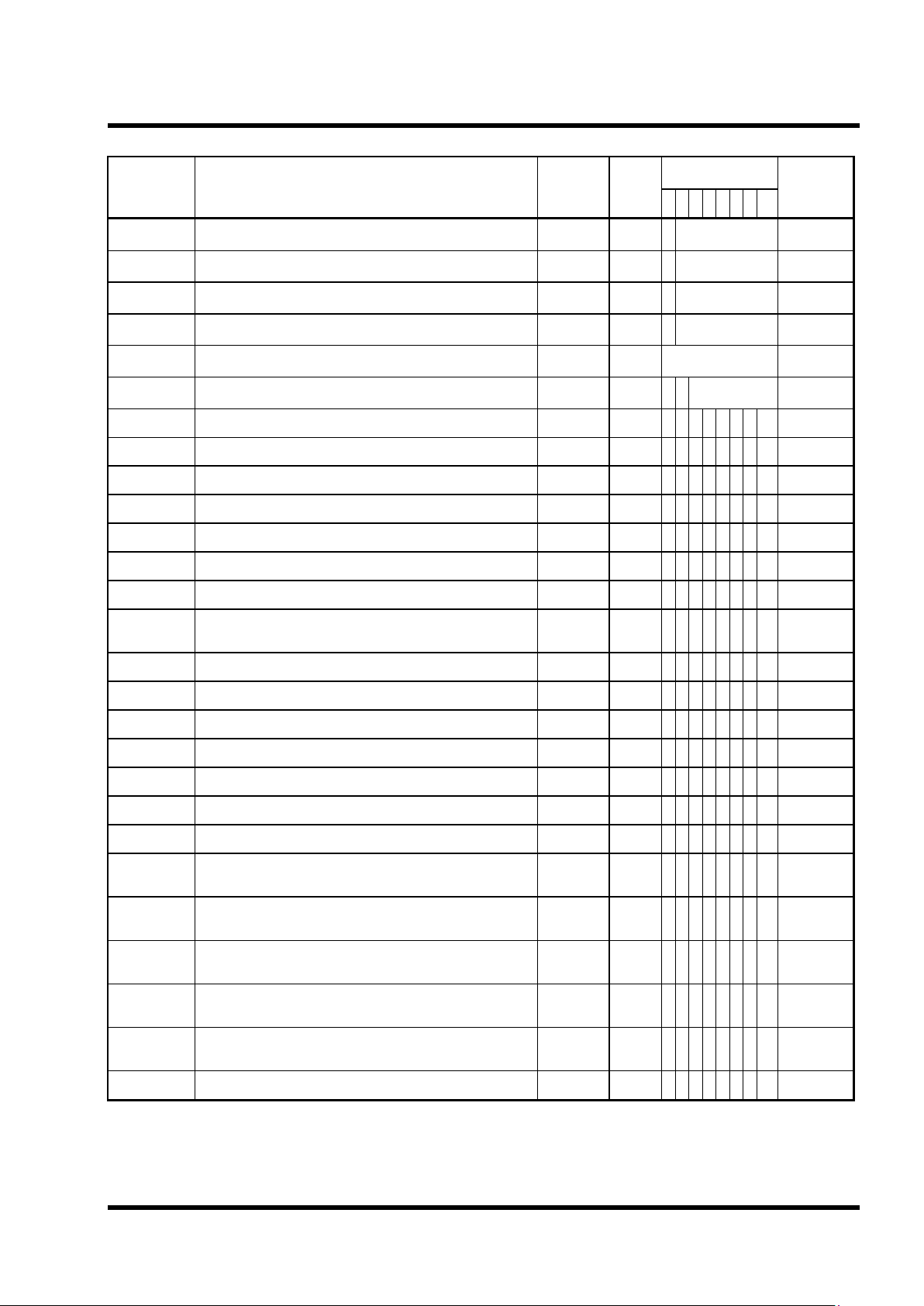
GMS 84512 / 84524
2 - 9
Address Register Name SYMBOLR/W
RESET VALUE
Page
76543210
00DE
H
PWM4 DATA REGISTER PWMR4 W -
Undefined
3 - 35
00DF
H
PWM5 DATA REGISTER PWMR5 W -
Undefined
3 - 35
00E0
H
PWM6 DATA REGISTER PWMR6 W -
Undefined
3 - 35
00E1
H
PWM7 DATA REGISTER PWMR7 W -
Undefined
3 - 35
00E2
H
PWM8 DATA REGISTER HIGH PWM8H R/W
Undefined
3 - 36
00E3
H
PWM8 DATA REGISTER LOW PWM8L R/W --
Undefined
3 - 36
00E4
H
PWM CONTROL REGISTER1 PWMCR1 R/W 00000000 3 - 37
00E5
H
PWM CONTROL REGISTER2 PWMCR2 R/W ---00000 3 - 37
00E6
H
INTERRUPT MODE REGISTER IMOD R/W --000000 4 - 4
00E8
H
INTERRUPT ENABLE REGISTER LOW IENL R/W 00000-- - 4 - 3
00E9
H
INTERRUPT REQUEST FLAG REGISTER LOW IRQL R/W 00000-- - 4 - 4
00EA
H
INTERRUPT ENABLE REGISTER HIGH IENH R/W 00000000 4 - 3
00EB
H
INTERRUPT REQUEST FLAG REGISTER HIGH IRQH R/W 00000000 4 - 4
00EC
H
INTERRUPT INTERVAL DETERMINATION
CONTROL REGISTER
IDCR R/W -----000 3 - 40
00ED
H
INTERRUPT INTERVAL DETERMINATION REGISTER IDR R 00000000 3 - 38
00F0
H
OSD 1st LINE HORIZONTAL POSITION REGISTER HDP1 W --000000 3 - 47
00F1
H
OSD 2nd LINE HORIZONTAL POSITION REGISTER HDP2 W --000000 3 - 47
00F2
H
OSD 3rd LINE HORIZONTAL POSITION REGISTER HDP3 W --000000 3 - 47
00F3
H
OSD 1st LINE VERTICAL POSITION REGISTER VDP1 W -0000000 3 - 47
00F4
H
OSD 2nd LINE VERTICAL POSITION REGISTER VDP2 W -0000000 3 - 47
00F5
H
OSD 3rd LINE VERTICAL POSITION REGISTER VDP3 W -0000000 3 - 47
00F6
H
OSD 1st LINE DISPLAY MODE, CHARACTER SIZE,
SMOOTHING FUNCTION SELECTION REGISTER
DMSS1 W -0000000 3 - 44
00F7
H
OSD 2nd LINE DISPLAY MODE, CHARACTER SIZE,
SMOOTHING FUNCTION SELECTION REGISTER
DMSS2 W -0000000 3 - 44
00F8
H
OSD 3rd LINE DISPLAY MODE, CHARACTER SIZE,
SMOOTHING FUNCTION SELECTION REGISTER
DMSS3 W -0000000 3 - 44
00F9
H
OSD OUTPUT and BACKGROUND CONTROL
REGISTER
OSDCON1 W 00000000 3 - 48
00FA
H
I/O POLARITY CONTROL and OSD OSCILLATION
CONTROL REGISTER
OSDCON2 W 00000000 3 - 48
00FC
H
OSD RAM ( 2 page ) ACCESSABLE REGISTER PG2R** R/W -------0 3 - 43
¡Ø-: Not used *0: READ only for bit 0 *6: READ only for bit 6
¡Ø Write Only Register can not be accessed by bit manipulation instruction.
** : OSD RAM area (2-page) can be accessed by LDM,SET1
Page 24
GMS 84512 / 84524
2 - 10
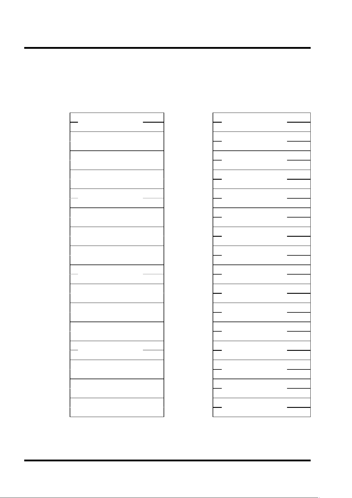
VECTOR AREA
FFC0
H
( L ) FFE0
H
( L )
FFC1
H
( H ) FFE1
H
( H )
FFC2
H
( L ) FFE2
H
( L )
FFC3
H
( H ) FFE3
H
( H )
FFC4
H
( L ) FFE4
H
( L )
FFC5
H
( H ) FFE5
H
( H )
FFC6
H
( L ) FFE6
H
( L )
FFC7
H
( H ) FFE7
H
( H )
FFC8
H
( L ) FFE8
H
( L )
FFC9
H
( H ) FFE9
H
( H )
FFCA
H
( L ) FFEA
H
( L )
FFCB
H
( H ) FFEB
H
( H )
FFCC
H
( L ) FFEC
H
( L )
FFCD
H
( H ) FFED
H
( H )
FFCE
H
( L ) FFEE
H
( L )
FFCF
H
( H ) FFEF
H
( H )
FFD0
H
( L ) FFF0
H
( L )
FFD1
H
( H ) FFF1
H
( H )
FFD2
H
( L ) FFF2
H
( L )
FFD3
H
( H ) FFF3
H
( H )
FFD4
H
( L ) FFF4
H
( L )
FFD5
H
( H ) FFF5
H
( H )
FFD6
H
( L ) FFF6
H
( L )
FFD7
H
( H ) FFF7
H
( H )
FFD8
H
( L ) FFF8
H
( L )
FFD9
H
( H ) FFF9
H
( H )
FFDA
H
( L ) FFFA
H
( L )
FFDB
H
( H ) FFFB
H
( H )
FFDC
H
( L ) FFFC
H
( L )
FFDD
H
( H ) FFFD
H
( H )
FFDE
H
( L ) FFFE
H
( L )
FFDF
H
( H ) FFFF
H
( H )
* This vector area is used in both BRK and TCALL 0 instruction
not used
SERIAL I/O
Basic Interval Timer
Watch Dog Timer
EXT. INT 3
Timer 3
Timer1
V-Sync Interrupt
1mS Interrupt
Timer 2
Timer 0
EXT. INT 2
EXT. INT1
On Screen Display
not used
RESET
TCALL 15
TCALL 14
TCALL 13
TCALL 12
TCALL 11
TCALL 10
TCALL 9
TCALL 8
TCALL 7
TCALL 6
TCALL 5
TCALL 4
TCALL 3
TCALL 2
TCALL 1
TCALL 0 *
Page 25

GMS84512/84524 USER’ S MANUAL
Table of Contents
1. Overview
2. CPU
3. Peripheral Function
4. Control Function
5. Support Tool
6. Appendix
Page 26
GMS 84512 / 84524
3- 1
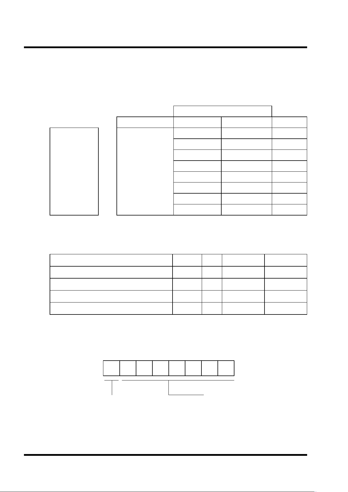
3.1 PORT
There are 6-ports in this device.
You can use these ports an digital I/O or 2nd function I/O
3.1.1 R0 PORT
8-bit I/O port including direction register and port data register (IOA Type)
l Register Structure and Description
Register Name Symbol R/W Address Initial Value
R0 I/O Direction Register R0DD W 00C1
H
0000 0000
R0 PORT Data Register R0 R/W 00C0
H
Not initialized
If output mode port is read, the read data is R0 register data. And if input mode port is read, the
read data is R0 pin data.
Assign the direction of R0 port
(R0DD0) is assigned to R00 port)
0 : Input
1 : Output
<00C1H>
R0DD
R0 PORT I/O DIRECTION REGISTER
7
R0DD76R0DD65R0DD54R0DD43R0DD32R0DD21R0DD10R0DD0
W W W W W W W W
Initial Value when RESET
[ 0000 0000 ]
Port R0 output data
Initial Value when RESET
[Not initialized ]<00C0H>
R0
R0 PORT DATA REGISTER
7
R076R065R054R043R032R021R010R00
R/W R/W R/W R/W R/W R/W R/W R/W
Page 27
GMS 84512 / 84524
3 - 2
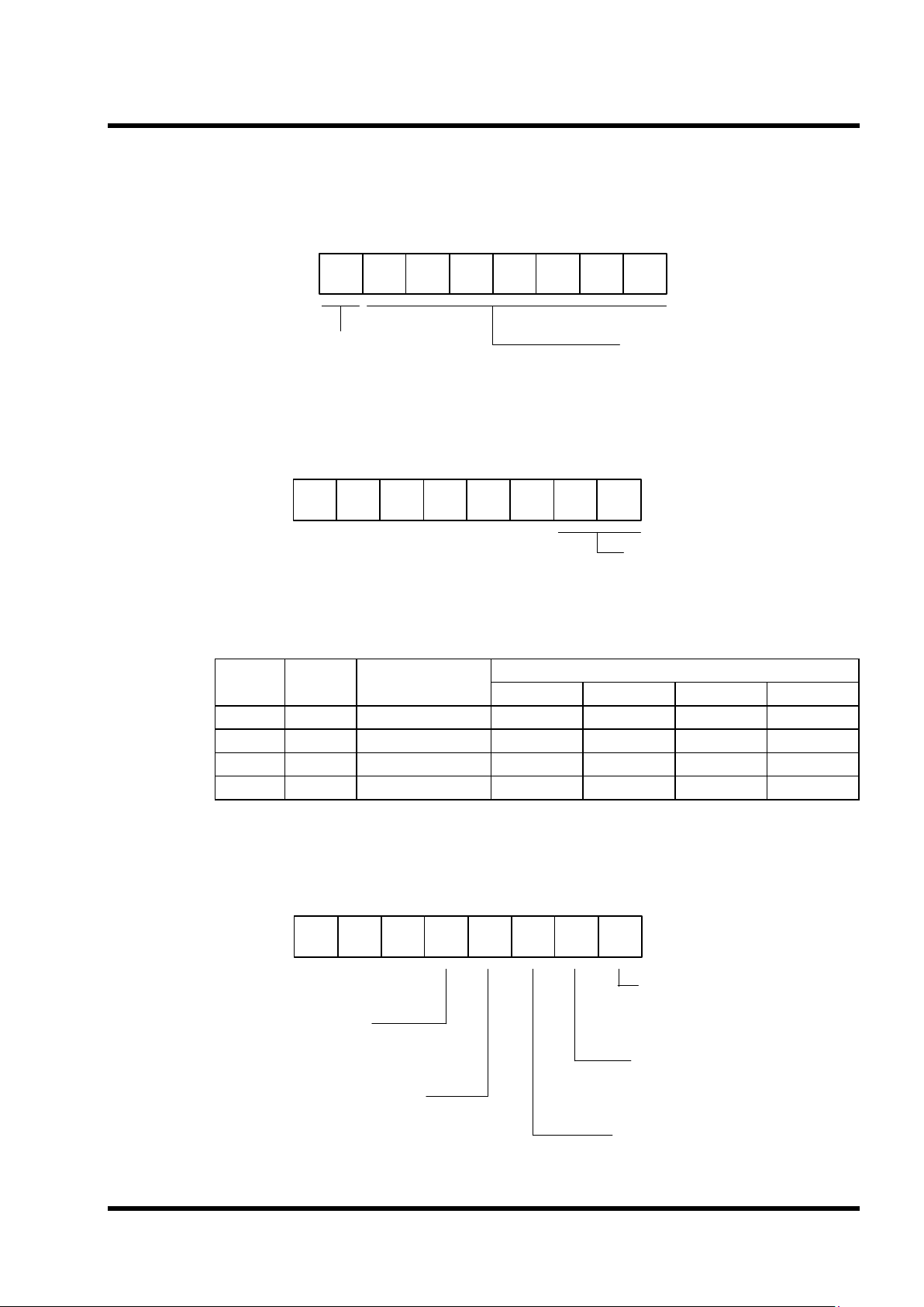
3.1.2 R1 PORT
You can use the R17 port as input mode only, but others as input or output mode.
Selection Mode
Pin Name Port Selection 2nd Function Type
0 R10 R10 ( I/O ) R10 ( I/O )
IOA
1 R11 R11 ( I/O ) R11 ( I/O )
IOA
2 R12 R12 ( I/O ) R12 ( I/O )
IOA
3 R13 R13 ( I/O ) R13 ( I/O )
IOA
4 R14 R14 ( I/O ) R14 ( I/O )
IOA
5 R15/ Cin1 R15 ( I/O ) Cin1 ( I )
IOC
6 R16/ Cin2 R16 ( I/O ) Cin2 ( I )
IOC
7 R17/ Cin0/ INT3 R17 ( I ) Cin0/ INT3 ( I )
IC
l Register Structure and Description
Register Name Symbol R/W Address Initial Value
R1 I/O Directin Register R1DD W 00C3
H
0000 0000
R1 Port Data Register R1 R/W 00C2
H
Not initialized
A/D COMP. Input CH. Selection Register CIS w 00D7
H
---- --00
Port Function Selection Register FUNC W 00CA
H
---0 0000
R1
PORT
Not used
Assign the direction of R1 port
(R1DD0) is assigned to R10 port)
0 : Input
1 : Output
<00C3H>
R1DD
R1 PORT I/O DIRECTION REGISTER
7
-
6
R1DD65R1DD54R1DD43R1DD32R1DD21R1DD10R1DD0
-
W W W W W W W
Initial Value when Reset
[ -000 0000 ]
Page 28
GMS 84512 / 84524
3- 3
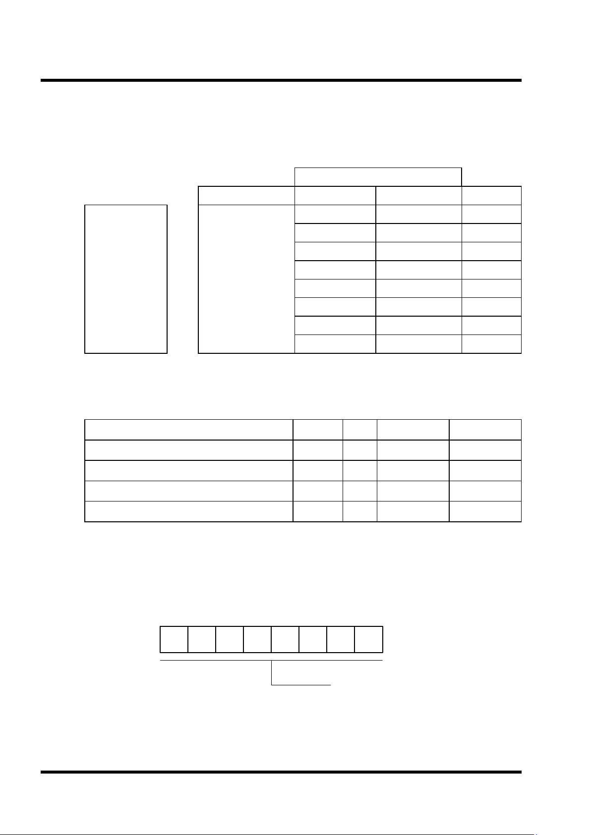
PORT Selection
CIS1 CIS0 Channel
R15/ Cin1 R16/ Cin2
R17/ Cin0/ INT3R35/ Sin/ Cin3
0 0 Channel 0 (Cin0) R15 R16 Cin0/ INT3 R35/ Sin
0 1 Channel 1 (Cin1) Cin1 R16 R17/ Cin0 R35/ Sin
1 0 Channel 2 (Cin2) R15 Cin2 R17/ Cin0 R35/ Sin
1 1 Channel 3 (Cin3) R15 R16 R17/ Cin0 Cin3
Input data when read Port R1 output data
Initial Value when Reset
[ Not initialized ]<00C2H>
R1
R1 PORT DATA REGISTER
7
-
6
R165R154R143R132R121R110R10
R R/W R/W R/W R/W R/W R/W R/W
R27 / EC3 Selection
0 : R27 ( I/O )
1 : EC3 ( Input )
R17 / INT3 Selection
0 : R17 ( Input )
1 : INT3 ( Input )
R26 / EC2 Selection
0 : R26 ( I/O )
1 : EC2 ( Input )
R31/ INT2 Selection
0 : R31 ( Input )
1 : INT2 ( Input )
R30 / INT1 Selection
0 : R30 ( Input )
1 : INT1 ( Input )
<00CAH>
FUNC
PORT FUNCTION SELECTION REGISTER
7
-
6
-
5
-
4
EC3S3EC2S2INT3S1INT2S0INT1S
- - -
W W W W W
Initial value when MCU Reset
[ ---0 0000 ]
A/D COMP. INPUT CHANNEL SELECTION
Initial Value when Reset
[ ---- --00 ]
<00D7H>
CIS
7
-6-
5
-4-3-
2
-
1
CIS10CIS0
- - - - - -
W W
Analog input channel selection
00 : CIN0
01 : CIN1
10 : CIN2
11 : CIN3
Page 29
GMS 84512 / 84524
3 - 4
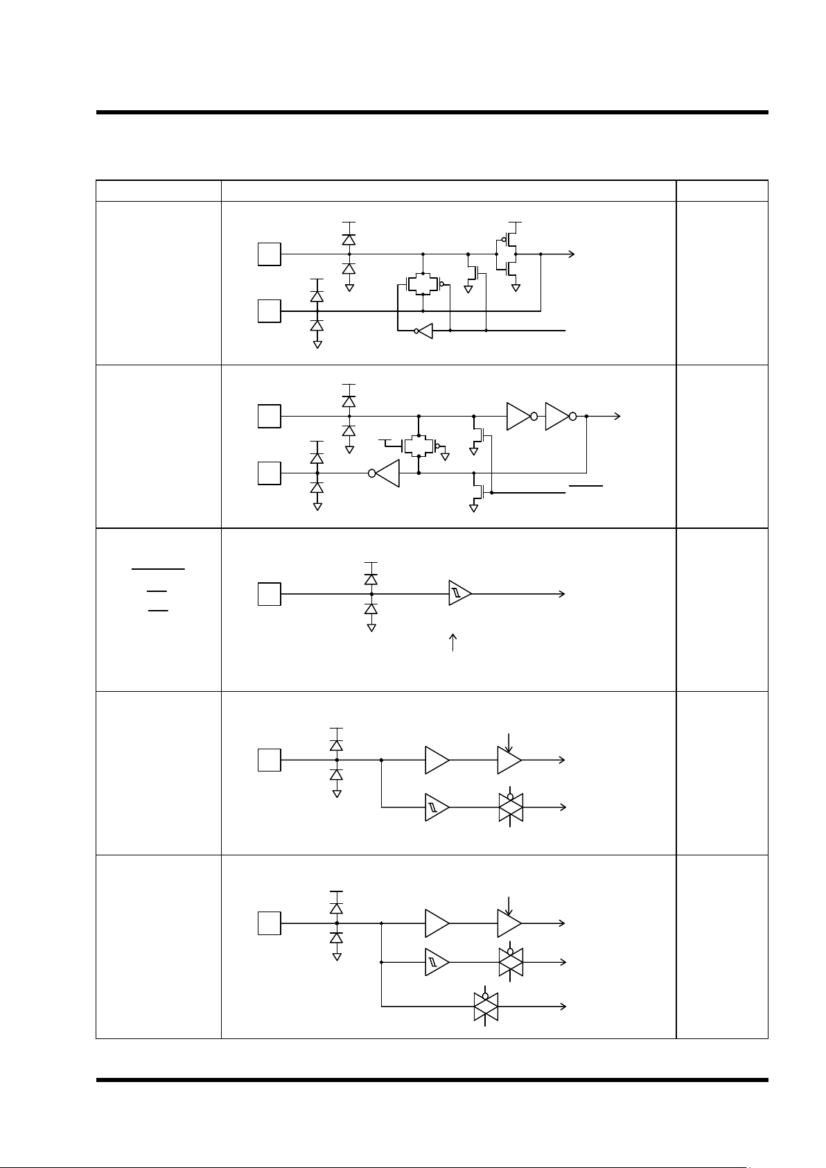
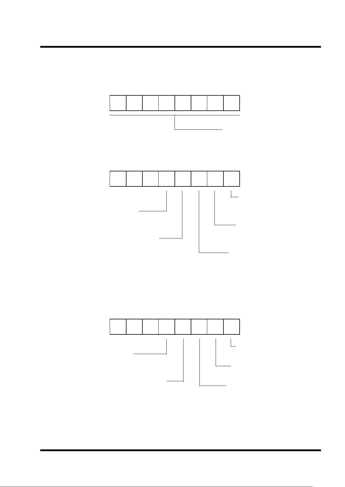
3.1.3 R2 PORT
8- BIT I/O Port
Selection Mode
Pin Name Port Selection 2nd Functin Type
0 R20 R20 ( I/O ) R20 ( I/O )
IOA
1 R21 R21 ( I/O ) R21 ( I/O )
IOA
2 R22 R22 ( I/O ) R22 ( I/O )
IOA
3 R23 R23 ( I/O ) R23 ( I/O )
IOA
4 R24 R24 ( I/O ) R24 ( I/O )
IOA
5 R25/ T2048 R25 ( I/O ) T2048 ( O )
IOD
6 R26/ EC2 R26 ( I/O ) EC2 ( I )
IOB
7 R27/ EC3 R27 ( I/O ) EC3 ( I )
IOB
l Register Structure and Description
Register Name Symbol R/W Address Initial Value
R2 I/O Direction Register R2DD W 00C5
H
0000 0000
R2 Port Data Register R2 R/W 00C4
H
Not initialized
Port Function Selection Register FUNC W 00CA
H
---0 0000
PWM Control Register 2 PWMCR2R/W 00E5
H
---0 0000
R2
PORT
Assign the direction of R2 port
R2DD is assigned to R20 port
0 : Input
1 : Output
<00C5H>
R2DD
R2 PORT I/O DIRECTION REGISTER
7
R2DD76R2DD65R2DD54R2DD43R2DD32R2DD21R2DD10R2DD0
W W W W W W W W
Initial value when MCU Reset
[ 0000 0000 ]
Page 30
GMS 84512 / 84524
3- 5
Port R2 output data
Initial value when MCU Reset
[ Not initialized ]<00C4H>
R2
R2 PORT DATA REGISTER
7
R276R265R254R243R232R021R210R20
R/W R/W R/W R/W R/W R/W R/W R/W
R27 / EC3 Selection
0 : R27 ( I/O )
1 : EC3 ( Input )
R17 / INT3 Selection
0 : R17 ( Input )
1 : INT3 ( Input )
R26 / EC2 Selection
0 : R26 ( I/O )
1 : EC2 ( Input )
R31/ INT2 Selection
0 : R31 ( Input )
1 : INT2 ( Input )
R30 / INT1 Selection
0 : R30 ( Input )
1 : INT1 ( Input )
<00CAH>
FUNC
PORT FUNCTION SELECTION REGISTER
7
-
6
-
5
-
4
EC3S3EC2S2INT3S1INT2S0INT1S
- - -
W W W W W
Initial value when MCU Reset )
[ ---0 0000 ]
PWM OUTPUT CONTROL REGISTER 2
Initial value when MCU Reset
[ ---0 0000 ]
<00E5H>
PWMCR2
7
-
6
-
5
-
4
T20483POL22POL11EN70EN6
- - -
R/W R/W R/W R/W R/W
R25/ T2048 Selection
0 : R25
1 :T2048 (Output rectangular wave(T=2048uS)
7-bit PWM OUTPUT Polarity
0 : Positive Polarity
1 : Negative Polarity
14-bit PWM Output Polarity
0 : Positive poarity
1 : Negative Polarity
R36/ PWM7 Selection
0 : R36
1 : PWM7
R37/ PWM6 Selection
0 : R37
1 : PWM6
Page 31

GMS 84512 / 84524
3 - 6
3.1.4 R3 PORT
You can use lower 2-bits(R31, R30) of R3 port as input mode only. But others as input or output
mode
Selection Mode
Pin Name Port Selection 2nd Function Type
0 R30/ INT1 R30 ( I ) INT1 ( I )
IB
1 R31/ INT2 R31 ( I ) INT2 ( I )
IB
2 R32/ PWM8 R32 ( I/O ) PWM8 ( O )
IOD
3 R33/ Sout R33 ( I/O ) Sout ( I/O )
IOG
4 R34/ Sclk R34 ( I/O ) Sclk ( I/O )
IOG
5 R35/ Sin/ Cin3 R35 ( I/O ) Sin/ Cin3 ( I )
IOE
6 R36/ PWM7 R36 ( I/O ) PWM7 ( O )
IOF
7 R37/ PWM6 R37 ( I/O ) PWM6 ( O )
IOF
l Register Structure and Description
Register Name Symbol R/W Address Initial Value
R3 I/O Direction Register R3DD W 00C7
H
0000 0000
R3 Port Data Register R3 R/W 00C6
H
Not Initialized
Port Function Selection Register FUNC W 00CA
H
---0 0000
Serial I/O Mode Register SIOM R/W 00D8
H
-000 0001
PWM Control Register 1 PWMCR1R/W 00E4
H
0000 0000
PWM Control Regsiter 2 PWMCR2R/W 00E5
H
---0 0000
R3
PORT
Not used
Port R3 I/O Direction Register
( R3DD2 is assigned to R32 port )
0 : Input
1 : Output
<00C7H>
R3DD
PORT R3 I/O DIRECTION REGISTER
7
R3DD76R3DD65R3DD54R3DD43R3DD32R3DD2
1
-
0
-
W W W W W W
- -
Initial value when MCU Reset
[ 0000 00-- ]
Page 32

GMS 84512 / 84524
3- 7
Input data when read
Port R3 Output Data
Initial value when MCU Reset
[ Not initialized ]<00C6H>
R3
R3 PORT DATA REGISTER
7
R376R365R354R343R332R32
1
-
0
-
R/W R/W R/W R/W R/W R/W R R
R27 / EC3 Selection
0 : R27 ( I/O )
1 : EC3 ( Input )
R17 / INT3 Selection
0 : R17 ( Input )
1 : INT3 ( Input )
R26 / EC2 Selection
0 : R26 ( I/O )
1 : EC2 ( Input )
R31/ INT2 Selection
0 : R31 ( Input )
1 : INT2 ( Input )
R30 / INT1 Selection
0 : R30 ( Input )
1 : INT1 ( Input )
<00CAH>
FUNC
PORT FUNCTION SELECTION
7
-
6
-
5
-
4
EC3S3EC2S2INT3S1INT2S0INT1S
- - -
W W W W W
Initial vlaue when MCU Reset
[ ---0 0000 ]
R42/ PWM3 Selection
0 : R42
1 : PWM3
PWM CONTROL REGISTER 1
Initial value when MCU Reset
[ 0000 0000 ]
<00E4H>
PWMCR1
7
EN56EN45EN34EN23EN12EN01EN80CNT
R/W R/W R/W R/W R/W R/W R/W R/W
R41/ PWM4 Selection
0 : R41
1 : PWM4
R40/ PWM5 Selection
0 : R40
1 : PWM5
R43/ PWM2 Selection
0 : R43
1 : PWM2
R44/ PWM1 Selection
0 : R44
1 : PWM1
R45/ PWM0 Selection
0 : R45
1 : PWM0
R32/ PWM8 Selection
0 : R32
1 : PWM8
14-bit / 7-bit PWM Count Start/Stop
0 : Count Start
1 : Count Stop
Page 33

GMS 84512 / 84524
3 - 8
Port Selection
SM1 SM0 Function Selection
R33/ Sout R34/ Sclk
R35/ Sin/ Cin3 *
0 0 - R33 R34 R35
0 1 Send Mode Sout Sclk R35
1 0 Receive Mode R33 Sclk Sin
1 1 - R33 R34 R35
R35 port will not operate, when Cin3 is operating as A/D input port.
PWM CONTROL REGISTER 2
Initial value when MCU Reset
[ ---0 0000 ]
<00E5H>
PWMCR2
7
-
6
-
5
-
4
T20483POL22POL11EN70EN6
- - -
R/W R/W R/W R/W R/W
R25/ T2048 Selection
0 : R25
1 :T2048 (Output rectangular(T=2048ys))
7-bit PWM Output Polarity
0 : Positive Polarity
1 : Negative Polarity
14-bit PWM Output Polarity
0 : Positive Polarity
1 : Negative Polarity
R36/ PWM7 Selection
0 : R36
1 : PWM7
R37/ PWM6 Selection
0 : R37
1 : PWM6
SERIAL I/O MODE REGISTER
Initial value when MCU Reset
[ -000 0001 ]
<00D8H>
SIOM
7
-
6
IOSW5SM14SM03SCK12SCK01SIOST0SIOSF
-
R/W R/W R/W R/W R/W R/W R
Serial Transmission ClockSelection
00 : PS3 ( 1uS )
01 : PS4 ( 2uS )
10 : PS5 ( 4uS )
11 : External Clock
Serial Operation Mode
01 : Receive Mode (Sclk, Sout)
10 : Send Mode (Sclk, Sin)
etc. : R33,R34,R35 Selection
Serial Transmission Start
0 : Invalid
1 : Transmission Start(Reset after cycle )
erial transmission status FLAG
0 : In transmitting
1 : End of transmission
Serial Input Selection
0 : Input via Sin
1 : Input via Sout
Page 34

GMS 84512 / 84524
3- 9
3.1.5 R4 PORT
6-Bit output port.
Selection Mode
Pin Name Port Selection Function Selection Type
0 R40/ PWM5 R40 ( O ) PWM5 ( O )
OB
1 R41/ PWM4 R41 ( O ) PWM4 ( O )
OB
2 R42/ PWM3 R42 ( O ) PWM3 ( O )
OB
3 R43/ PWM2 R43 ( O ) PWM2 ( O )
OB
4 R44/ PWM1 R44 ( O ) PWM1 ( O )
OB
5 R45/ PWM0 R45 ( O ) PWM0 ( O )
OB
l Register Structure and Description
Register Name Symbol R/W Address Initial Value
R4 Port Data Register R4 R/W 00C8
H
Not initialized
PWM Control Register PWMCR1R/W 00E4
H
0000 0000
R4
PORT
Port R4 output data
Initial value when MCU Reset
[ Not initialized ]<00C8H>
R4
R4 PORT DATA REGISTER
7
-
6
-
5
R454R443R432R421R410R40
- -
R/W R/W R/W R/W R/W R/W
Not used
R42/ PWM3 Selection
0 : R42
1 : PWM3
PWM CONTROL REGISTER 1
Initial value when MCU Reset
[ 0000 0000 ]
<00E4H>
PWMCR1
7
EN56EN45EN34EN23EN12EN01EN80CNT
R/W R/W R/W R/W R/W R/W R/W R/W
R41/ PWM4 Selection
0 : R41
1 : PWM4
R40/ PWM5 Selection
0 : R40
1 : PWM5
R43/ PWM2 Selection
0 : R43
1 : PWM2
R44/ PWM1 Selection
0 : R44
1 : PWM1
R45/ PWM0 Selection
0 : R45
1 : PWM0
R32/ PWM8 Selection
0 : R32
1 : PWM8
14-bit / 8-bit PWM Count Start/Stop
0 : Count Start
1 : Count Stop
Page 35

GMS 84512 / 84524
3 - 10
3.1.6 R5 PORT
4-Bit output only port.
Selection Mode
Pin Name Port Selection 2nd Function Type
0
R50/ R R50 ( O ) R ( O )
OA
1 R51/ G R51 ( O ) G ( O )
OA
2 R52/ B R52 ( O ) B ( O )
OA
3 R53/ Y R53 ( O ) Y ( O )
OA
l Register Structure and Description
Register Name Sumbol R/W Address Initial Value
R5 Port Data Register R5 R/W 00C9
H
Not initialized
OSD Output/ BACKGROUND Control Register
OSDCON1
W 00F9
H
0000 0000
R5
PORT
Port R5 Output Data
Initial value when MCU Reset
[ Not initialized ]<00C9H>
R5
R5 PORT DATA REGISTER
7
-
6
-
5
-4-
3
R532R521R510R50
- - - -
R/W R/W R/W R/W
Not used
Background and Edge Color Selecton
Initial value when MCR Reset
[ 0000 0000 ]
<00F9H>
OSDCON1
OSD OUTPUT & BACKGROUND CONTROL
7
OY6OB5OG4OR
3
OSDON
2
BB1BG0BR
W W W W W W W W
R53/ Y Selection
0 : R53
1 : Y
R52/ B Selection
0 : R52
1 : B
R50/ R Selection
0 : R50
1 : R
R51/ G Selection
0 : R51
1 : G
OSD Output Control
0 : Disable
1 : Enable
Page 36

GMS 84512 / 84524
3 - 11
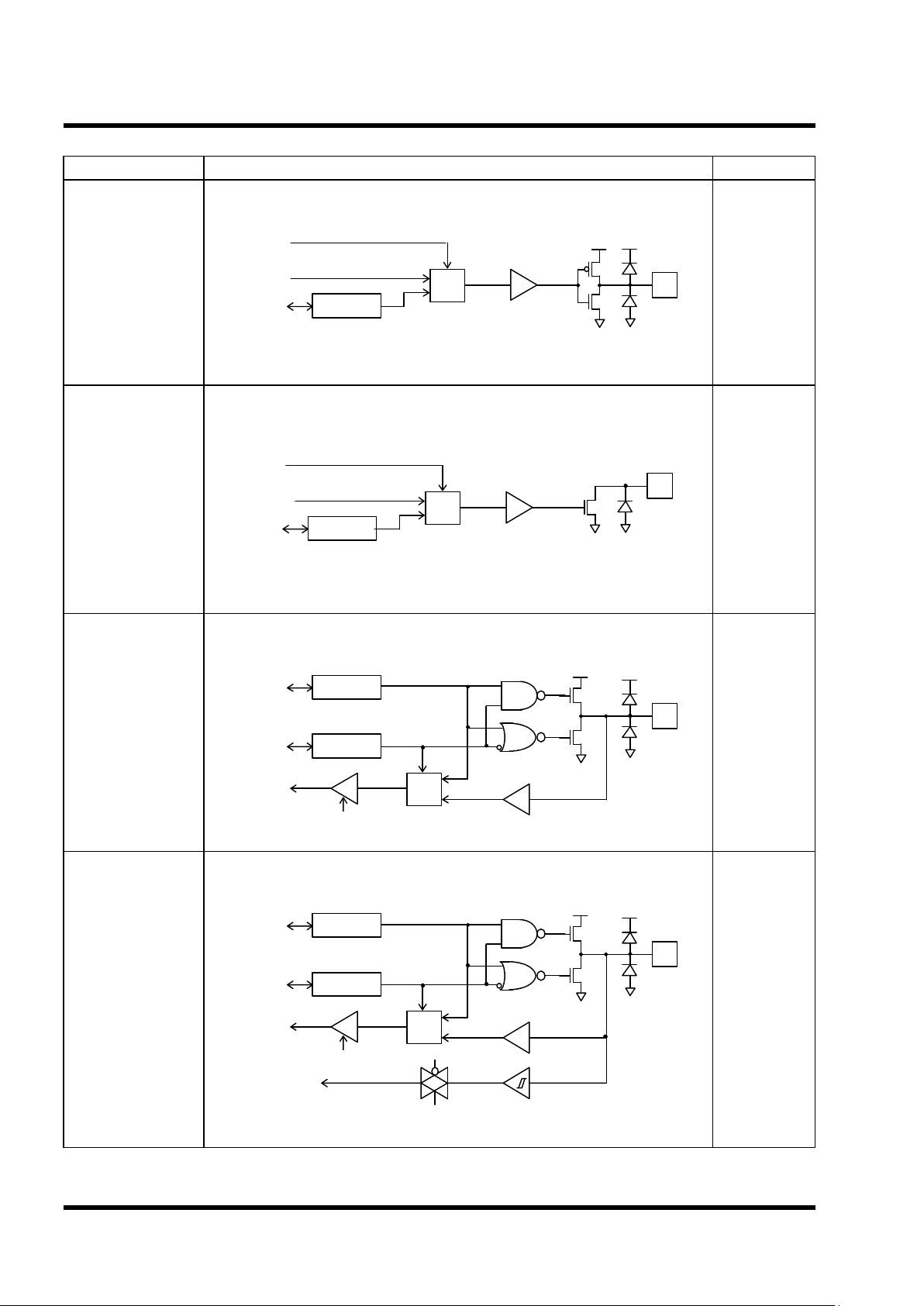
3.2 CLOCK GENERATION CIRCUIT
The clock generation circuit of GMS84512/84524 is consist of oscillation circuit for CPU clock, prescaler for
peripheral clock and Basic Interval Timer Clock. Basic Interval Timer for reference time, and water Dog
Timer for detecting S/W overrun.
8
WDTON
PRESCALER (11)
ENPCK
WDTCL
to RESET
CIRCUIT
IFWDT
IFBIT
BTCL
PERIPHERAL CIRCUIT
Internal System Clock
Clock Pulse Generator
7
0
Basic Interval Timer(8)
MUX
21
CKCTLR
0
OSC
Circuit
8
11
650
50
WDT
CL
COMPARATOR
6
6
Watch Dog Timer(6)
7
WDTR
5
FIG.3.2.1 Clock Generation Circuit Block Diagram
Internal DATA BUS
6
3 4
Page 37

GMS 84512 / 84524
3 - 12
3.2.1 Oscillation Circuit
The clock signal incoming from crystal oscillator or ceramic resonator via Xin and Xout, or from
external clock via Xin is supplied to Clock Pulse Generator and Prescaler
Internal System Clock for CPU is made by Clock Pulse Generator, and several peripheral clock is
devided by prescaler
Clock Generation circuit of Crystal Oscillator or Ceramic Resonator is shown in Fig.3.2.2
¨ç Clock Generation Circuit by Crystal Oscillator or Ceramic Resonator
¨è Clock generator circuit by external clock
FIG. 3.2.2. Clock Generation Circuit
¡ÚWhen STOP Mode, Oscillation Stops,
Xin pin is High-Impedance, and Xout pin is going to High level state.
Xin
Cin
GND
Cout
Xout
Xin
External Clock
Open
Xout
Page 38

GMS 84512 / 84524
3 - 13
3.2.2 PRESCALER
Prescaler is consisted of 11-bit binary counter, and input clock is supplied by oscillation circuit.
Frequency divided output from each bit of prescaler is used as peripheral clock.
FIG. 3.2.3 Configuration of Prescaler
TABLE 3.2.1 Frequency-Divided Outputs of Prescaler
f
EX
( §Ö)
PS1 PS2 PS3 PS4 PS5 PS6 PS7 PS8 PS9 PS10 PS11
Interval
4 §Ö 2 §Ö 1§Ö 500§Õ 250§Õ 125§Õ 62.5§Õ31.25§Õ15.63§Õ 7.18§Õ3.91§Õ
Period
250nS 500nS 1uS 2uS 4uS 8uS 16uS 32uS 64uS 128uS 256uS
Interval
6§Ö 3§Ö 1.5§Ö 750 §Õ 375§Õ 187.5§Õ93.75§Õ46.88§Õ23.44§Õ11.72§Õ5.86§
Period
166.7nS 333.3nS 666.7nS 1.3uS 2.7uS 5.3uS 10.7uS 21.3uS 42.7uS 85.3uS 170.7uS
l
Peripheral
ENPCK
fex
B.I.T.
PS2 PS3 PS4 PS5 PS6 PS7 PS8 PS9 PS10 PS11
PS21 PS2 PS3 PS4 PS5 PS6 PS7 PS8 PS9 PS10
PS11
8
11
4
6
B.I.T. CLEAR ( When writing )
0 : B.I.T. FREE-RUN
1 : B.I.T. CLEAR ( Auto reset after 1-cycle )
B.I.T input clock selection (When writing)
000 : PS4 ( 2uS) 100 : PS8 ( 32uS)
001 : PS5 ( 4uS) 101 : PS9 ( 64uS)
010 : PS6 ( 8uS) 110 : PS10 ( 128uS )
011 : PS7 ( 16 uS) 111 : PS11 ( 256uS)
Initial value when MCU Reset
CKCTLR : [ --01 0111 ]
CLOCK CONTROL REGISTER
7
-6-
5
WDTON
4
ENPCK
3
BTCL2BTS21BTS10BTS0
W W W W W W W W
Peripheral Clock Enable ( When writing )
0 : Peripheral Clock Stop
1 : Peripheral Clock Supply
WDT function control (When writing)
0 : 6bit TIMER
1 : WATCH-DOG TIMER
B.I.T. count value (When read)
<00CEH>
CKCTLR
Page 39

GMS 84512 / 84524
3 - 14
Peripheral Hardware Clock control Function
Peripheral Clock supplied from prescaler can be stopped by ENPCK. Peripheral hardware clock control bit
of CKCTLR Register.(However, PS11 cannot be stopped by ENPCK).
3.2.3 Basic Interval Timer
There is 8-bit binary counter is Basic Interval Timer. It operates as following function.
-Reference Time interval interrupt request as timer.
-B.I.T. can be read
( Note; The writing at same address overwrites the CKCTLR.)
-Clock supply of Watch Dog Timer.
FIG. 3.2.4 Configuration of Basic Interval Timer
PS4
- -
WDTON
ENPCK
BTCL BTS2 BTS1 BTS0
CKCTLR
bit7 bit6
bit5 bit4
bit3 bit2 bit1 bit0
B.I.T.
PS5
PS6
PS7
PS8
PS9
PS10
PS11
MUX
IFBIT
Data BUS
Data BUS
8
6
Same address
when read, it can be read as counter
value. When write, it can be write as
control register.
Page 40

GMS 84512 / 84524
3 - 15
Control of Basic Interval Timer
Basic Interval Timer is Free Running Timer, but it can be cleared by setting BTCL ( Bit 3 of clock control
register). Initial state (after Reset) of BTCL is “0”, and if it is set to “1” it is auto-cleared after 1 machine cycle.
l Input clock selection of Basic Interval Timer and Reference Time interrupt interval
Input clock of Basic Interval Timer is selected by BTS2~BTS0(Bit2~0 of clock control register)among
the prescaler outputs. Reference time interval interrupt is generated by BIT overflow.
TABLE 3.2.2 Input clock selection of Basic Interval Timer and reference time interrupt interval
(@4MHz)
BTS2 BTS1 BTS0 B.I.T. Input Clock Period Reference Time Interrupt Period
0 0 0
PS4 ( 2uS) 512uS
0 0 1
PS5 ( 4uS) 1,024uS
0 1 0
PS6 ( 8uS) 2,048uS
0 1 1
PS7 ( 16uS) 4,096uS
1 0 0
PS8 ( 32uS) 8,192uS
1 0 1
PS9 ( 64uS) 16,384uS
1 1 0
PS10 ( 128uS) 32,768uS
1 1 1
PS11 ( 256uS) 65,536uS
B.I.T. input clock selection
see Table 3.3.2
B.I.T. CLEAR ( When writing )
0 : B.I.T. Free-run
1 : B.I.T. Clear ( auto cleared after 1 machine cycle )
Initial value when MCU Reset
CKCTLR : [ --01 0111 ]
CLOCK CONTROL REGISTER
7
-6-
5
WDTON4ENPCK
3
BTCL2BTS21BTS10BTS0
W W W W W W W W
<00CEH>
CKCTLR
B.I.T Input Clock Selection ( When writing )
Initial value when MCU Reset
CKCTLR : [ --01 0111 ]
CLOCK CONTROL REGISTER
7
-6-
5
WDTON
4
ENPCK
3
BTCL2BTS21BTS10BTS0
W W W W W W W W
B.I.T. count value (When read)
<00CEH>
CKCTLR
Page 41

GMS 84512 / 84524
3 - 16
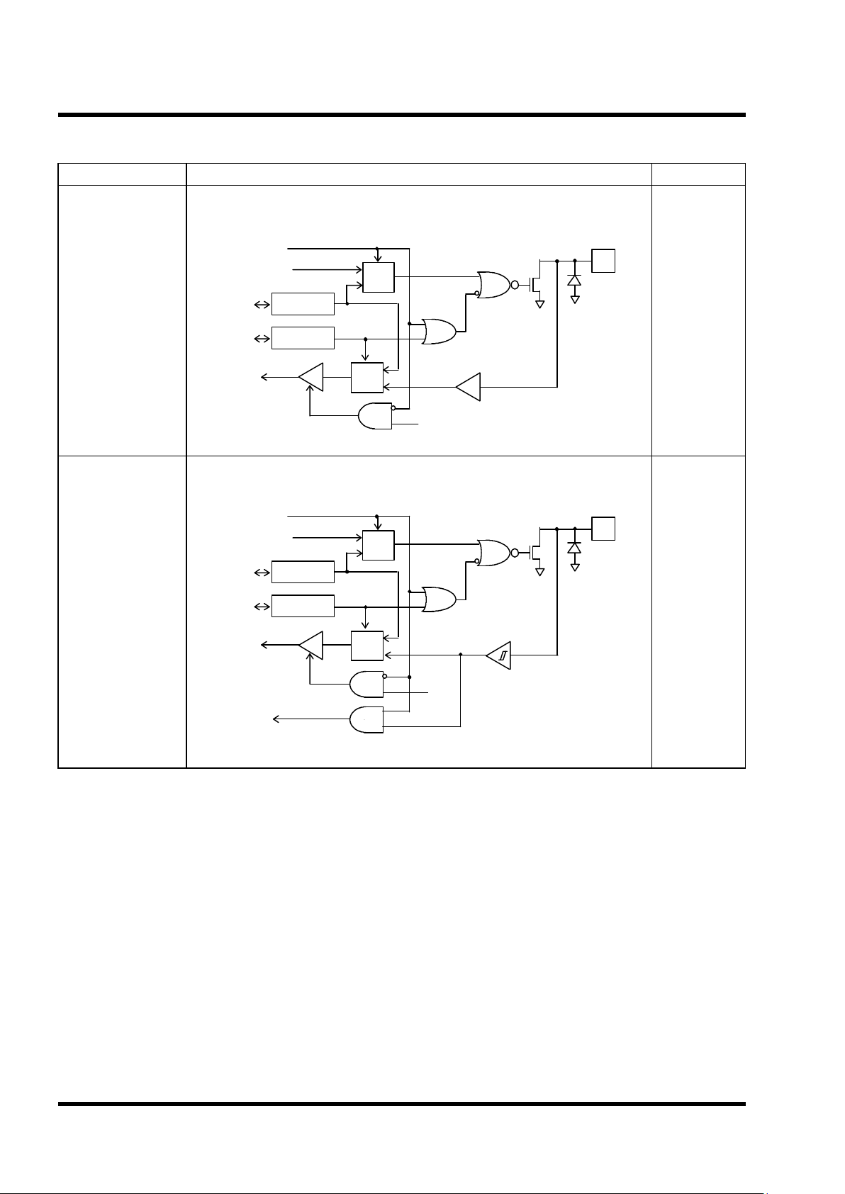
l Reading of Basic Interval Timer
Basic Interval Timer Register can be read and interval up to 65ms can be measured
(Note : The writing at same address overwrites the CKCTLR.)
3.2.4 Watch Dog Timer
Watch Dog Timer is consist of 6-bit Binary Counter, 6-Bit Comparator and Watch Dog Timer
Register(WDTR)
IFWDT is generated when counter value equals to WDTR, it can be used as S/W interrupt or
MCU reset (Watch Dog Function) signal.
Initial value when MCU Reset
Not initialized
BASIC INTERVAL TIMER REGISTER
7
bit76bit6
5
bit54bit4
3
bit32bit21bit10bit0
R R R R R R R R
B.I.T.count value ( When read)
<00CEH>
BITR
IFBIT
WDTON
to Reset
Data BUS
IFWDT
CLR
6
6-bit COMPARATOR
FIG. 3.2.4 Configuration Watch Dog Timer
0
WDT0 WDT1
WDT2 WDT3 WDT45WDT5
6-bit Counter
WDTR
0
WDTR0WDTR1WDTR2WDTR3WDTR4WDTR5WDT
CL
7
Page 42

GMS 84512 / 84524
3 - 17
l Control of WDT
WDTcan be used as 6-bit Timer or Watch Dog Timer according to WDTON ( Bit 5 of CKCTLR).
WDT is cleared by setting WDTCL (Bit 6 WDTR) to “1”.
< Notice >
1: After WDTON=1, maximum error of Timer is are one of period of IFBIT.
2: Because 6-bit counter begin to count after MCU Reset
the Watch Dog Timer should be enabled after clearing it.
l Interval of WDT Interrupt
Interval of WDT Interrupt is decided by Basic Interval Timer Interrupt an WDTR
That is, Interval of = ( WDTR value ) X ( IFBIT interval ).
WDT control (When writing)
0 : 6-bit Timer
1 : Watch-Dog Timer
Initial value when MCU Reset
CKCTLR : [ --01 0111 ]
CLOCK CONTROL REGISTER
7
-6-
5
WDTON
4
ENPCK
3
BTCL2BTS21BTS10BTS0
W W W W W W W W
<00CEH>
CKCTLR
WDT CLEAR
0 : WDT Free-Run
1 : WDT CLEAR (Auto reset after 1 cycle )
Interval of WDT
IFWDT period= ( WDTR value )X( IFBIT interval )
<00CFH>
WDTR
WATCH-DOG TIMER REGISTER
7
-
6
WDTCL
5
WDTR
5
4
WDTR
4
3
WDTR
3
2
WDTR
2
1
WDTR
1
0
WDTR
0
-
W W W W W W W
Initial value when MCU Reset
[ -011 1111 ]
Page 43

GMS 84512 / 84524
3 - 18
l Selection of WDT clock and maximum interval of WDT interrupt
Input clock of WDT is IFBIT, so WDT interval is decided by BTS2~BTS1. Interval of WDT interrupt
become maximum value.
< Notice >
Do not use WDTR=0 for MCU not to be Reset state always.
TABLE 3.2.2 Selection of WDT clock and maximum interval of WDT interrupt
(@ 4MHz)
BTS2 BTS1 BTS0 B.I.T. Input Clock WDT Input Clock IFWDT max. interval
0 0 0
PS4 ( 2uS) 512 uS 32,256 uS
0 0 1
PS5 ( 4uS) 1,024 uS 64,512 uS
0 1 0
PS6 ( 8uS) 2,048 uS 129,024 uS
0 1 1
PS7 ( 16uS) 4,096 uS 258,048 uS
1 0 0
PS8 ( 32uS) 8,192 uS 516,096 uS
1 0 1
PS9 ( 64uS) 16,384 uS 1,032,192 uS
1 1 0
PS10 ( 128uS) 32,768 uS 2,064,384 uS
1 1 1
PS11 ( 256uS) 65,536 uS 4,128,768 uS
Page 44

GMS 84512 / 84524
3 - 19
3.3 TIMER
Timer of GMS84512/84524 is 8-bit binary counter is consisted of Timer0(T0). Timer1(T1), Timer2(T2),
Timer(T3), Timer Data Register(TDR0~TDR3). Timer Mode Register(TM0, TM2) and control circuit.
T0, T1 is each 8-bit interval Timer and can be used as a 16-bit intrval Timer.
T2, T3 is each 8-bit interval timer/event counter and can be used as a 16-bit interval timer/event counter
3.3.1 OPERATION MODE OF TIMER
l Operating mode of T0, T1
T0 T1
l 8-bit Interval Timer l 8-bit Interval Timer
l 16-bit Interval Timer
l Operating mode ofT2, T3
T2 T3
-. 8-bit Interval Timer
-. 8-bit Event Counter
-. 8-bit Interval Timer
-. 8-bit Event Counter
-. 16-bit Interval Timer
-. 16-bit Event Counter
When T2, T3 are used as event counter the relevant Port Mode Register Value should be
assigned to select EC2 or EC3.
When T2, T3 are used as event counter, TDR value should be initialized to “FFH” because
Timer count value is cleared if it equals to TDR value
Note) At the Reset Routine, TDR0 ~ TDR3 are should be initialized by software. (Except 00H)
R27 / EC3 Selection
0 : R27 ( I/O )
1 : EC3 ( Input )
R26 / EC2 Selection
0 : R26 ( I/O )
1 : EC2 ( Input )
<00CAH>
FUNC
PORT FUNCTION SELECTION REGISTER
7
-
6
-
5
-
4
EC3S3EC2S2INT3S1INT2S0INT1S
- - -
W W W W W
Initial value (When MCU Reset
[ ---0 0000 ]
Page 45

GMS 84512 / 84524
3 - 20
ck
PS6
PS4
PS2
T0CN
T1ST
T0ST
PS8
PS6
PS4
2
PS2
TDR0
Data BUS
FIG. 3.3.1 Configuration TIMER0,TIMER1
16bit Mode
16bit Mode
MUX
8
TM0
7
1 03 25 4
-
6
TDR1
IFT0
IFT1
8
8
Comparator 0
8
Comparator 1
Data Reg. 1
Data Reg. 0
8
T 0
8
T 1
8 8
Clear
ck
Clear
1
MUX
0
1
MUX
0
MUX
2
ck
PS6
PS4
EC3
T2CN
T3ST
T2ST
PS8
PS6
PS4
2
EC2
TDR2
TM2
Data BUS
FIG. 3.3.2 Configuration of TIMER2,TIMER3
16bit Mode
16bit Mode
MUX
7
8
1 03 25 4
-
6
TDR3
IFT2
IFT3
8
8
Comparator 2
8
Comparator 3
Data Reg. 3Data Reg. 2
8
T 2
8
T 3
8 8
Clear
ck
Clear
1
MUX
0
1
MUX
0
MUX
2
Page 46

GMS 84512 / 84524
3 - 21
TIMER MODE REGISTER 0
T1 Input Clock Selection
00 : Connection to T0 (16bit Mode )
01 : PS2 ( 500uS)
10 : PS4 ( 2uS)
11 : PS6 ( 8uS)
T0 Input Clock Selection
00 : PS2 ( 500uS)
01 : PS4 ( 2uS)
10 : PS6 ( 8uS)
11 : PS8 ( 32uS)
Initial Value when MCU Reset
[ -000 0000 ]
<00D0H>
TM0
7
-
6
T1ST5T1SL14T1SL03T0ST2T0CN1T0SL10T0SL0
-
R/W R/W R/W R/W R/W R/W R/W
T0 Start/Stop control
0 : Count Stop
1 : Counting start after clearing T0
T0 Start/Stop control
0 : COUNT Stop
1 : COUNT Start
T1 Start/Stop control
0 : Cout Stop
1 : Counting start after clearing T1
* Don't care in 16bit Mode
TIMER MODE REGISTER 2
T3 Input Clock Selection
00 : Connection to T2 ( 16bit Mode )
01 : Input external clock source(EC3)
10 : PS2 ( 500uS)
11 : PS4 ( 2uS)
T2 Input Clock Selection
00 : Input external clock source(EC2)
01 : PS2 ( 500uS)
10 : PS4 ( 2uS)
11 : PS6 ( 8uS)
Initial value when MCU Reset
[ -000 0000 ]
<00D1H>
TM2
7
-
6
T3ST5T3SL14T3SL03T2ST2T2CN1T2SL10T2SL0
-
R/W R/W R/W R/W R/W R/W R/W
T2 Start/Stop Control
0 : Count Stop
1 : Counting start after clearing T2
T2 Start/Stop Control
0 : Count Stop
1 : Count Start
T3 Start/Stop control
0 : Count Stop
1 : Counting start after clearing T3
* Don't care in 16bit Mode
TIMER0 ~ TIMER3 DATA REGISTER
Initial value when MCU Reset
[ Not Initialized ]
<00D2H>
TDR0
7
TDR0
7
6
TDR0
6
5
TDR0
5
4
TDR0
4
3
TDR0
3
2
TDR0
2
1
TDR0
1
0
TDR0
0
R/W R/W R/W R/W R/W R/W R/W R/W
( WRITE)
Modulo Data Write of T0
Modulo Data Write of T1
Modulo Data Write of T2
Modulo Data write T3
( READ )
T0 Count Value Read
T1 Count Value Read
T2 Count Value Read
T3 Count Value Read
<00D3H>
TDR1
<00D4H>
TDR2
<00D5H>
TDR3
Page 47

GMS 84512 / 84524
3 - 22
TABLE 3.3.1 Timer resolutin and maximum count at fIN=4MHz
8-bit TIMER Mode 16-bit TIMER Mode
Resolution( ck ) max.count Resolution( ck ) max. count
PS2 ( 0.5§Á ) 128 §Á PS2 ( 0.5§Á) 32,768 §Á
PS4 ( 2§Á) 512 §Á PS4 ( 2§Á) 131,072 §Á
PS6 ( 8§Á) 2,048 §Á PS6 ( 8§Á) 524,288 §Á
PS8 ( 32§Á) 8,192 §Á PS8 ( 32§Á) 2,097,152 §Á
PS2 ( 0.5§Á) 128 §Á PS2 ( 0.5§Á) 32,768 §Á
T2
PS4 ( 2§Á) 512 §Á PS4 ( 2§Á) 131,072 §Á
PS6 ( 8§Á) 2,048 §Á PS6 ( 8§Á) 524,288 §Á
PS2 ( 0.5§Á) 128 §Á
( Note )
T1
PS4 ( 2§Á) 512 §Á
Operation As Upper 8-Bit of T0
PS6 ( 8§Á) 2,048 §Á
PS2 ( 0.5§Á) 128 §Á
( Note )
PS4 ( 2§Á) 512 §Á
Operation As Upper 8-Bit of T2
3.3.2 Operation of TIMER0, TIMER1
T0 ( T1 ) is consisted of 8-bit Binary Up-Counter. If T0 or T1 counter value become equal to Tdr0(or
TDR1) value, it is cleared to 00H, and Interrupt request (IFT0 or IFT1) is generated.
Timer
T0
T3
Interval Period
InterruptInterruptInterrupt
MATCHMATCHMATCH
ClearClearClear
00
H
IFT0
FIG 3.3.3 Operation of TIMER0 ,TIMER1
T0 VALUE
TDR0 VALUE
Page 48

GMS 84512 / 84524
3 - 23
l Any of the PS2, PS4, PS6 or PS8 can be selected as the clock source of T0 by bit1(T0SLI)
and bit0(T0SL0) of TM0. Andy of the PS2, PS4, PS6 or overflow of T0 can be selected as
the clock source of T1 by bit5(T1SL1) and bit4(T1SL0) of TM0.
l The operation of T0, T1 is controlled by bit3(T0ST), bit2(T0CN) and bit6(T1ST) of TM0. T0CN
controls count stop/start without clearing counter. T0ST and T1ST control count stop/start.
In order to enable timer to count-up, T0CN, T0ST and T1St should become “1”. After clearing
T0, T1 in order to count-up. T0st or T1ST should become “0” for a moment and return to “ 1”.
l The 16-bit interval timer is selected by assigning bit5(T1SL1) and bit4(T1SL0) to “0”.)
At 16-bit timer mode, IFT0 interrupt only is valid. It is prefered to write to the TDR in
non counting timer in order to protect undesirable interrupt.
CountCount StopCountStop
“0” “1” Start
“0” “1” Clear & Start
InterruptInterrupt
MATCHMATCH
ClearClearClear
00
H
IFT0
FIG 3.3.4 START/ STOP Control of Timer0
T0 VALUE
TDR0 VALUE
T0ST
COUNTER
T0CN
Page 49

GMS 84512 / 84524
3 - 24
3.3.2 Operation of TIMER2, TIMER3
l T2 ( T3 ) is consisted of 8-bit Binary Up-Counter. If T2(T3) counter value become equal to
TDR2(TDR3) value, it is cleared to 00H and interrupt request (IFT2 or IFT3) is generated.
l Any of the PS2, PS4, PS6 or external event input can be selected as the clock source of T2
by bit1(T2SL1) and bit0(T2SL0) of TM0. Any of the PS2, PS4 external event input or
overflow of T2 can be selected as the clock source of T1 by bit5(T3SL1) and bit4(T3SL0) of
TM0. If input clock is selected as external event input (EC2 or EC3), T2 and T3 operates as
8-bit event counter.
l The operation of T2, T2 is controlled by bit3(T2ST), bit2(T2CN) and bit6(T3ST) of TM2.
controls count stop/start without clearing counter. T2ST and T3ST control count stop/start.
order to enable timer to count-up T2CN, T2ST and T3ST should become “1”, After clearing
T0,T1 in order to count-up. T2ST or T3ST should become “0” for a moment and return to “ 1”
Interval Period
InterruptInterruptInterrupt
MATCHMATCHMATCH
ClearClearClear
00
H
IFT2
FIG 3.3.5 Operation of TIMER2 ( or TIMER3)
T2 VALUE
TDR2 VALUE
Page 50

GMS 84512 / 84524
3 - 25
l The 16-bit interval timer is selected by assigning bit5(T3SL1) and bit4(T3SL0) to “0”. At
16-bit timer mode, iIFT2 interrupt only is valid. It is prefered to write to the TDR in non counting timer, in order to protect undesirable interrupt. If the input clock is selected among
PS2, PS4 and PS6, T2 and T3 operate as 16-bit interval timer, while if EC2 operate as 16-bit
event/counter.
< Notice >
1. On counting the reading value of TDR is counted value
2. 16-bit Mode, when data are read I the middle of Timer operation, the prior upper 8 bit data
are read. Next the lower 8-bit data are read, and then the upper 8 bit data are read once
again. If the earlier read upper 8-bit data are matched with the later read upper 8 bit data,
16-bit data are read correctly. If not, caution should be taken in the selection of upper
8-bit data.
( Example )
1 ) Upper 8 bit Read 0A 0A
2 ) Lower 8 bit Read FF 01
3 ) Upper 8 bit Read 0B 0B
¡é ¡é
0AFF 0B01
CountCount StopCountStop
“0” “1” Start
“0” “1” Clear & Start
InterruptInterrupt
MATCHMATCH
ClearClearClear
00
H
IFT2
FIG 3.3.6 START/ STOP Control of Timer2
T2 VALUE
TDR2 VALUE
T2ST
COUNTER
T2CN
Page 51

GMS 84512 / 84524
3 - 26
3.4 A/D COMPARATOR
A/D comparator has an 5-bit resolution, and input is possible up to 4 channel. A/D comparator
is consisted of analog input multiplexer, 5-bit D/A conversion circuit, sample & holder and control
circuit
FIG.3.4.1 is a block diagram of A/D comparator
3.4.1 A/D COMPARATOR
Following produce is used.
- Write CIS register to select analog input channel.
- After writing CMR(ADCM0~4) to select reference voltage, set ADEN(bit7 of CMR) to “1” to
start A/D comparision..
< Notice > CMRcan’t be used with Bit Manipulation instruction and setting the reference
voltage and starting A/D comparision can be used at same time..
- A/D Comparision processing needs 16machine cycle(8us)
- The result of comparision is stored in COR(bit6 of CMR).
That is, if <input voltage > reference voltage>, COR=1
if <input voltage < reference voltage>, COR=0
Data BUS
ADEN
Vref
6 7
2
FIG. 3.4.1 Block Diagram of A/D Comparator
COMPARATOR
CMR
5
ADCM
3
ANALOG
INPUT
MU
LTIPLEXER
5-bit D/A C.
Cin3
RESISTER LADDER
ADENCOR
-
ADCM
4
ADCM0ADCM1ADCM
2
CIS
1 0
52
-
+
Cin2
Cin1
Cin0
OUTPUT
LATCH
Page 52

GMS 84512 / 84524
3 - 27
Port Selection
CIS1 CIS0 Function Selection
R15/ Cin1 R16/ Cin2
R17/ Cin0/ INT3R35/ Sin/ Cin3
0 0 Channel 0 (Cin0) R15 R16 Cin0/ INT3 R35/ Sin
0 1 Channel 1 (Cin1) Cin1 R16 R17/ Cin0 R35/ Sin
1 0 Channel 2 (Cin2) R15 Cin2 R17/ Cin0 R35/ Sin
1 1 Channel 3 (Cin3) R15 R16 R17/ Cin0 Cin3
l The Calculation of Reference Voltage
Reference Voltage ( Vref ) = { 2
X
( Value of ADCM) + 1 } X Vdd/64
A/D COMP. INPUT CHANNEL SELECTION REGISTER
Initial value when MCU Reset
[ ---- --00 ]
<00D7
H
>
CIS
7
-6-
5
-4-3-
2
-
1
CIS10CIS0
- - - - - -
W W
Analog input channel selection
00 : CIN0
01 : CIN1
10 : CIN2
11 : CIN3
A/D COMPARATOR MODE REGISTER
Initial value when MCU Reset
[ 00-0 0000 ]
<00D6
H
>
CMR
7
ADEN6COR
5
-
4
ADCM
4
3
ADCM
3
2
ADCM
2
1
ADCM
1
0
ADCM
0
W R
-
W W W W W
Reference Voltage Selection
00000 : Vdd/ 64
10000 : 33Vdd/ 64
00001 : 3Vdd/ 64 10001 : 35Vdd/ 64
00010 : 5Vdd/ 64 10010 : 37Vdd/ 64
| |
01111 : 31Vdd/ 64 11111 : 63Vdd/ 64
A/D Comparison Result
0 : Input Voltage <Reference Voltage
1 ; Input Voltage >Reference Voltage
A/D Comparision Control
0 : A/D Comparision Stop
1 ; A/D Comparision Start
Page 53

GMS 84512 / 84524
3 - 28
3.5 Serial I/O
The serial I/O is 8-bit clock sychronous type and is consisted of serial I/O register, serial I/O mode
register, clock selection circuit octal counter and control circuit. The Sout pin is degined to Input
and Output. So serial I/O interface can be operated with minimum two pin.
3.5.1 Serial I/O Data Register
Serial I/O Data Register SIORis a 8-bit Shift Register. First LSB is send or is received.
Initial value when MCU Reset
[ Not initialized ]
<00D9H>
SIOR
7
D76D65D54D43D32D21 D10D0
R/W R/W R/W R/W R/W R/W R/W R/W
At transmittion
Sending Data at Sending
Receiving Data at Receiving
FIG. 3.5.1 Block Diagram of Serial I/O
SIOR
1 03 25 47 6
Sclk
Octal Counter
Control
Circuit
Data BUS
SM0
SM1
2
MUX
PS5
PS4
PS3
IFSIO
Exclk
1
MUX
0
Sin
Sout
Data BUS
8
6
67 0
SIOM
SM0 SOSFSIOSTSCK0SCK1
-
IOSW SM1
Page 54

GMS 84512 / 84524
3 - 29
3.5.2 Serial I/O Mode Register
This register controls serial function. According to SCK1, SCK0 internal clock or external clock
can be used.
l Port Selection According to Serial I/O Mode
Port Selection
SM1 SM0 Function Selection
R33/ Sout R34/ Sclk
R35/ Sin/ Cin3 *
0 0 - R33 R34 R35
0 1 Sending Mode Sout Sclk R35
1 0 Receiving Mode R33 Sclk Sin
1 1 - R33 R34 R35
* If Cin3 is used as A/D comparator input channel, R35 port do not operate as output..
l Selection of Serial input pin with the IOSW
When receiving mode, serial input pin is selected by IOSW. That, if IOSW=0, R35/Sin is
selected. If IOSW=1, R33/Sout
SERIAL I/O MODE REGISTER
Initial value when MCU Reset
[ -000 0001 ]
<00D6H>
SIOM
7
-
6
IOSW5SM14SM03SCK12SCK01SIOST0SIOSF
-
R/W R/W R/W R/W R/W R/W R
Serial Transmission Clock Selection
00 : PS3 ( 1uS )
01 : PS4 ( 2uS )
10 : PS5 ( 4uS )
11 : External Clock
Serial Operation Mode
01 : Sending Mode (Sclk, Sout)
10 : Receiving Mode (Sclk, Sin)
Others : Selection of R33,R34,R35
Serial Transmission Start
0 : Invalid
1 : Start(After one SCK, becomes”0”)
Serial Transmission status FLAG
0 : Serial during transmission
1 : Serial finished
Serial Input Selection
0 : Via Sin
1 : Via Sout
Page 55

GMS 84512 / 84524
3 - 30
3.5.3 Data Transmission/Receving Timing
Serial transmission is started by setting SIOST(bit1 SIOM) to :”1”. After one cycle of SCK,
SIOST is cleared automatically to “0”. serial output data from 8-bit shift register is output at
folloing edge of Sclk. and input data is latched at rising edge of Sclek. When transmission Clock
is counted 8times, serial I/O counter is cleared as “0”. Transmission clock is halted in “H” state
and serial I/O interrupt (IFSIO) occursg.
3.5.4 Data Transmission/Receiving Method
- Select transmission/receiving mode
<Notice>
When external clock is used, the frequency should be less than 1MH and recommanded
duty is 50%.
- When sending Data to be send is written at SIOR.
- Set SIOST to “1” to start serial transmission.
<Notice >
If both transmission mode selection and starting transmission is performed
simultaneouslyit makes error.
- IFSIO is generated at completion and SIOSF is set to “1”. In SIO interrupt service routine
correct transmission should be tested.
- When receiving, receiving data is acquired by reading the SIOR.
D7D6D5D1 D4D3D2D0
D7D6D5D1 D4D3D2D0
Input Clock
Sclk
Latch
Output
IFSIO
Sin
Sout
SIOST
FIG. 3.5.1 Timing Diagram of Serial I/O
Page 56

GMS 84512 / 84524
3 - 31
3.5.5 The Method to Test Correct Transmission with S/W
0
1
Abnormal
SIOSF ?
FIG. 3.5.4 Serial Method to Teset Transmission.
Note) SE: Interrupt Enable Regist Low IENL ( Bit3 )
SR : Interrupt Request Flag Regist Low IRQL ( Bit3 )
Normal Operation
SE = 0
WRITE SIOM
Serial I/O Interrupt
SERVICE ROUTINE
1
0
OVERRUN ERROR
SR ?
Page 57

GMS 84512 / 84524
3 - 32
3.6 Pulse Width Modulation ( PWM )
The GMS84512/84524 is equipped with one 14-bit PWM(PWM8) and eight 7-bit
PWM(PWM0~PWM7).
The 14-bit resolution gives PWM8 the minium resolution bit width of 500ns(PS2=500ns, if
Xin=4MHz) and repeat period of 8,192uS. Each PWM0~PWM7 has a 7-bit resolution with min.
resolution bit width of 8uS ( PS6 ) and repeat period of 1,024uS.
l PWM Specification Table ( @ Xin =4MHz )
Specification 14-bit PWM 7-bit PWM
Resolution 14 bits 7 bits
Input Clock
0.5uS 8uS
1 Frame Cycle
8,192uS 1,024uS
PWMR7¡-PWMR0
7
1 03 25 4- 6
PWM7
PWM6
PWM5
PWM4
PWM3
PWM2
PWM1
EN0
Data BUS
FIG. 3.6.1 Block Diagram of 7-bit PWM & T2048
PWMCR2
5
1 03 2- 4- -
PWMCR1
8
1 03 25 47 6
PWMR7 EN7
PWMR1
PWMR2
PWMR3
PWMR4
PWMR5
PWMR6
EN6
EN5
EN4
EN3
EN2
EN1
Match
CNTB
PWM0
POL2
CNTB
7-bit Comparator
PS6
7
PWMR0
7
T F/F
7-bit Counter
T2048E
IF 1mS
T2048
Page 58

GMS 84512 / 84524
3 - 33
3.6.1 PWM8 (14-bit PWM )
When the PWM8 is used for output, first set the higher 8-bit of the PWM8H register, then the lower 6-bit of
the PWM6 register. The 14-bit data of PWM8 can be compare with the 14-bit comparator after lower 6-bit
data of PWM8 is transferred.
Data setting for PWM8(14-bit PWM)
l The PWM output pulse period is consist with 64(=26) high level area which is consist with 256(=28)low-
level area. First, the basic pulse is made by the data of PWM8H, then the position of pulse as long as
low level width(0.5uS) among 64 short pulse is determined by contents of PWM8L.
TABLE 3.6.1
BIT Sub-Frame(short pulse) position as long as low level area Pulse
Bit0 = “1”
S32, 1
Bit1 = “1”
S16, S48 2
Bit2 = “1”
S8 , S24, S40, S56 4
Bit3 = “1”
S4 , S12, S20, S28, S36, S44, S52, S60 8
Bit4 = “1”
S2 , S6 , S10, S14, S18, S22, S26, S30, S34, S38, S42, S46, S50, S54, S58,
S62
16
Bit5 = “1”
S1 , S3 , S5 , S7, S9, S11, S13, S15, S17, S19, S21, S23, S25, S27, S29, S31,
S33, S35, S37, S39, S41, S43, S45, S47, S49, S51, S53, S55, S57, S59, S61,
S63
32
EN8
Match
CNTB
PWM8
POL1
CNTB
Wpwm8L
Data BUS
FIG. 3.6.2 Block Diagram of 14-bit PWM
14-bit Comparator
PWM8L
6
1 03 25 4- -
PWMCR2
5
1 03 2- 4- -
14
14
14-bit Data Register
14
14-bit Counter
PS2
PWMCR1
8
1 03 25 47 6
8
8
PWM8H
1 03 25 47 6
Page 59

GMS 84512 / 84524
3 - 34
Basic Pulse Width ( 65uS)
: Sub-Frame with Added Pulse
Pulse Width = 65.5uS
Added Pulse Width( 0.5uS )
PWM Period ( 8,192 §Á)
Period of Basic Pulse ( 128uS )
Basic pulse width
FIG.3.6.3 Example output of the 14-bit PWM ( Polarity : Positive )
Added pulse
Number of Added Pulse ( PWM8L= 06H ):
6 ( S8,S16,S24,S40,S48,S56 )
Basic pulse width ( PWM8H= 82H ):
( 130 ) X 0.5 = 65uS
Initial value (at RESET)
[ Undefined ]
<00E2
H
>
PWM8H
7
D76D65D5
W
4D43D32D21D10
D0
Initial value (at RESET)
[ Undefined ]
<00E3
H
>
PWM8L
7
-6-
5
D5
W
4D43D32D21D10
D0
13
112011010090807160504030211100
S1
S0
S3
S2
S9S8 S61 S63
S62
S57S56S49S48S25S24 S41S40S17S16
Page 60

GMS 84512 / 84524
3 - 35
3.6.2 PWM0¡-PWM7 ( 7-bit PWM ¡¿ 8 CH. )
Each PWM0~PWM7 can be used for different PWM output by each 7-bit data register
(PWMR0~PWM7). The PWM pulse period is 1,024§Á and the width is (PWMR+1)¡¿T/128 .
(0<PWMR<127: Value of 7-bit PWM register data)
PWM0~PWM7 is positive, negative for output. The start point of output is spreaded wide,
so the flow of current is proper.
PWM0~PWM7 is port is N-MOS open drain.
3.6.3 PWMR0¡-PWMR7 REGISTER
PWMR0¡-PWMR7 are the data register to define 7-bit PWM pulse width and it has only write
. They are undefined at reset state.
Pulse Width( 1,024)
)
Pulse Width
Pulse Period( 1,024 §Á )
Pulse Width
¨ç
Positive Polarity ( POL2 = 0 )
Pulse Width = ( PWMR +1 )£¯128 ¡¿ 1,024 [§Á]
DUTY CYCLE = ( PWMR +1 )£¯128 ¡¿ 100 [ % ]
FIG. 3.6.4 Output Pulse of PWM0
¡-
PWM7
¨è
Negative Polarity ( POL2 = 1 )
Initial value (at RESET)
[ Undefined ]
PWMR0 ¡-PWMR7 DATA REGISTER
<00DAH>
PWMR0
7 6
¦¡
PWM0
D6
5
PWM0
D5
4
PWM0
D4
3
PWM0
D3
2
PWM0
D2
1
PWM0
D1
0
PWM0
D0
¦¡
W W W W W W W
Storage of each PWM data
<00DCH>
PWMR2
<00DEH>
PWMR4
<00E0H>
PWMR6
<00DBH>
PWMR1
<00DDH>
PWMR3
<00DFH>
PWMR5
<00E1H>
PWMR7
Page 61

GMS 84512 / 84524
3 - 36
3.6.4 PWM8H, PWM8L REGISTER
PWM register (PWM8H, PWM8L) are the data register to define 14bit PWM pulse width and it is
enable R/W. They are not fixed at reset state.
3.6.5 The control of 14-bit PWM
¨ç Write upper data to PWM8H (definition of basic pulse width)
¨è Write lower 6-bit data to PWM8L
¨é When data are written PWM8L, the 14-bit data of PWM8 is written to compare register so,
even if you will change the upper 8-bit of output data, you will write 6bit data to PWM8L again.
But when you will change the lower 6-bit of output data, you need not write the upper 8-bit to
PWM8H again..
¨ê Output polarity is determined by POL1.( bit2 of PWM control register 2)
Default is positive polarity.(POL1=0)
¨ë PWM8 port is selected by setting EN8(bit1 of PWM ontrol register1) to “1”,
so the wave of PWM is to be output.
¨ì If CNTB(bit6 of PWMCR1) is "0", Counter is operating, on the contrary if it is "1" count stops.
This have an effect on both of them.(14-bit PWM/7-bit PWM counter)
Initial Value (At Reset)
[ Undefined ]
PWM8H , PWM8L DATA REGISTER
<00E2H>
PWM8H
7 6
PWM8H7PWM8
H6
5
PWM8
H5
4
PWM8
H4
3
PWM8
H3
2
PWM8
H2
1
PWM8
H1
0
PWM8
H0
R/W R/W R/W R/W R/W R/W R/W R/W
Storage of 14-bit PWM upper 8-bit data
When PWM8L is written it is loaded in upper 8-bit of
14-bit comparator, so the width of basic pulse are
determined. When PWM8L is read, the
contents(PWM8L) of comparator is read.
Initial Value (At Reset)
[ Undefined ]
7 6
¡ª ¡ª
5
PWM8
L5
4
PWM8
L4
3
PWM8
L3
2
PWM8
L2
1
PWM8
L1
0
PWM8
L0
¡ª ¡ª
R/W R/W R/W R/W R/W R/W
The number and position for added-pulse of 64
basic pulse are determined
<00E3H>
PWM8L
Page 62

GMS 84512 / 84524
3 - 37
3.6.6 The Control of 7-bit PWM
¨ç Write 7-bit data to each PWM data register (PWMR0~PWMR7).
¨èDefine output polarity by POL2 (bit3 of PWMCR2(PWM control register2))
Positive polarity is determine by default. also this has effect an all 7bit PWM output
¨é If each PWM port is selected by setting EN0~EN7(bit2~bit7 of PWMCR1, bit1 and bit2 ofPWMCR2) to
"1".
¨ê If CNTB(bit0 of PWMCR1) is "0", counter is operating, on the contrary if it is “1” counter stops. This
has effect on all 14-bit PWM/7-bit PWM counter.
R42/ PWM3
0 : R42
1 : PWM3
PWM CONTROL REGISTER 1
Initial Value (at RESET)
[ 0000 0000 ]
<00E4H>
PWMCR1
7
EN56EN45EN34EN23EN12EN01EN80CNTB
R/W R/W R/W R/W R/W R/W R/W R/W
Select R41/ PWM4
0 : R41
1 : PWM4
Select R40/ PWM5
0 : R40
1 : PWM5
Select R43/ PWM
2 0 : R43
1 : PWM2
Select R44/ PWM1
0 : R44
1 : PWM1
R45/ PWM0 0 : R45
1 : PWM0
Stop/StartR32/
PWM8 0 : R32
1 : PWM8
14-bit / 8-bit PWM Count Stop/Start
COUNT Start 1 :
COUNT Stop
PWM CONTROL REGISTER 2
Initial Value (at RESET)
[ ---0 0000 ]
<00E5H>
PWMCR2
7
¦¡6¦¡
5
¦¡
4
T20483POL22POL11EN70EN6
¦¡ ¦¡ ¦¡
R/W R/W R/W R/W R/W
Start R25/ T2048
0 : R25
1 :T2048 (Period 2048 §Á rectangular pulse output select)
7-bit PWM OUTPUT Polarity
0 : Positive PolarityY
1 : Negative Polarity
14-bit PWM Output Polartity
0 : Positive Polarity
1 : Negative Polarity
Select R36/ PWM7
0 : R36
1 : PWM7
Select R37/ PWM6
0 : R37
1 : PWM6
Page 63

GMS 84512 / 84524
3 - 38
3.7. Interrupt Interval Measurement Circuit
GMS84512/84524 is equipped with distinct edge of input signal for 2 channel external interrupt
(INT1, INT2) and interrupt interval measurement circuit of evaluating distinct edge interval.
Interrupt interval measurement circuit is equipped with interrupt input multiplexer, 8bit binary upcounter measurement clock selection circuit, interrupt interval storage circuit and interrupt interval
measurement control register
3.7.1 Operation of Interrupt Interval Measurement Circuit
Interrupt interval measurement circuit stores the count value of 8-bit up counter to IDR(interrupt
interval data register) by selected edge of external interrupt input. And then it may clear 8-bit
up-counter, go on counting again. And the counter value of 8-bit up-counter is stored to IDR by
selected edge of second external interrupt input.
So, selected edge interval of external interrupt input is measured to PS8(32§Á) or PS9(64§Á).
Rising/Falling edge of interrupt input signal is selected by IEDS(External Interrupt Signal Edge
Selection)and width or period of input signal is measured by combination of selected edge.
External interrupt input signal is selected by FUNC(port function selection register)
Fig 3.7.2 and TABLE 3.7.1 show interrupt input signal edge selection and measurement interval.
8
Clear
32§Á
IDST
64§Á
Data BUS
FIG. 3.7.1 Configruation of interrupt interval measurement circuit
IDR
8
INT1
8-bit Up-Counter
IDCR
INT2
PS9
PS8
2 07
¡ª¡ª ¡ª ¡ª ¡ª
IDSTIDCKISEL
3
1
MUX
0
Interrupt Interval Data
Register
ck
Delay
Circuit
1
MUX
0
Data BUS
Page 64

GMS 84512 / 84524
3 - 39
TABLE 3.7.1 Measurement Interrupt Interval and Edge Selection
Sym
bol
IED*H IED*L
¨Í
1 0
¨Î
0 1
¨Ï
1 1
¨Ð
1 1
R27 / EC3 Selection
0 : R27 ( Input, Output )
1 : EC3 ( Input )
R17 / INT3 Selection
0 : R17 ( Input )
1 : INT3 ( Input )
R26 / EC2 Selection
0 : R26 ( Input, Output )
1 : EC2 ( Input )
R31/ INT2 Selection
0 : R31 ( Input )
1 : INT2 ( Input )
R30 / INT1 Selection
0 : R30 ( Input )
1 : INT1 ( Input )
<00CAH>
FUNC
PORT FUNCTION SELECTION REGISTER
7
¦¡
6
¦¡
5
¦¡
4
EC3S3EC2S2INT3S1INT2S0INT1S
¦¡ ¦¡ ¦¡
W W W W W
Initial Value (at RESET)
[ ---0 0000 ]
Edge selection of external INT input
signal.
00 : No Input Selection
01 : Falling Edge Selection
10 : Rising Edge Selection
11 : Both of Edge All Selection
<00CBH>
IEDS
EXT. INTERRUPT EDGE SELECTION REGISTER
7
¦¡
6
¦¡
5
IED3H4IED3L3IED2H2IED2L1IED1H0IED1L
¦¡ ¦¡
W W W W W W
Initial Value(at RESET)
[ --00 0000 ]
Period
Width of
Pulse
INT Input Signal
¨Í
¨Î
¨Ï
¨Ð
FIG 3.7.2 The Kind of Interrupt Interval
Page 65

GMS 84512 / 84524
3 - 40
3.7.2 Interrupt Interval Measurement Method
The following is a interrupt interval measurement method.
¨ç Select interrupt input port to be used by writing data to FUNC(00CA
H
)
¨è To measure interrupt interval, select the edge of interrupt input signal by writing data to
IEDS( 00CB
H
)
¨é Control to write data to IDCR (Interrupt interval measurement control register) .
When IDST(bit0 fo IDCR) is "1", counter is operating. If IDCK (bit1 of IDCR) selecting
measurement clock is "0", PS9(64§Á) is selected, otherwise PS8(32§Á) is selected.
If ISEL(bit of IDCR) selecting external interrupt input is "0", INT1 is selected, otherwise INT2
is selected.
¨ê If using edge of interrupt input signal is to be input automatically the value of counter is stored
to IDR(00EDH), after 1 machine cycle, counter is to be clear and go on count-up.
So, interrupt interval is measured continuously.
Interval Measurement Clock Selection
0 : 64§Á
1 : 32§Á
External INT. input selection
0 : INT1
1 : INT2
COUNTER Start/Stop Control
0 : Count Stop
1 : After Counter Clear Start Count-Up
Initial Value(at RESET)
[ ---- -000 ]
<00ECH>
IDCR
INTERRUPT INTERVAL DETERMINATION CONTROL REGISTER
7
¦¡
6
¦¡
5
¦¡4¦¡
3
¦¡
2
ISEL1IDCK0IDST
¦¡ ¦¡ ¦¡ ¦¡ ¦¡
R/W R/W R/W
No use
33
H
1F
H
After 1 Machine
Cycle
Start
Rising Edge
ClearClearClear
00
H
FIG 3.7.3 The example of Interrupt Interval Measurement
8-bit Counter
INT Input Signal
? 33
H
1F
H
IDR
Page 66

GMS 84512 / 84524
3 - 41
3.8 On Screen Display ( OSD )
3.8.1 OSD Overview
The OSD of GMS84512/84524 can display maxium 128 kinds of character or symbol to CRT screen,
basically GMS84512/84524 incorporates a 22 characters ¡¿3lines CRT display control circuit. If OSD
interrupt is to be used, maxium 12 lines can be displayed.
Especially, GMS84512/84524 is equipped with smoothing function and color edge function.
3.8.2 Feature of OSD
l OSD CLOCK : 4 §Ö ¡- 8
§Ö
l The Nnmber of Character: 128 characters ( include 2 test characters )
l Display Ability : 22 Character
¡¿
3 lines
( use OSD Interrupt : enable 12 lines )
l Character Size : 16 kinds ( every line unit )
l Character Color : 8 kinds ( every character unit )
l Font Configulation : 14
¡¿
18 Dots
l Display Position : Horizontal 61 steps, Vertical 128 step (every line unit)
l Display MOde : Character Mode, Background Mode
Color Edge Mode, Blanking Mode
( every line unit )
l Background Size : Domain of total screen, domain of line unit
l Background and Edge Color : 8 kinds
l
Smoothing Function
l OSD Oscillator Control Function
3.8.3 Configuration of OSD
The OSD of GMS84512/84524 is equipped with OSD oscillator, timing circuit, display position
register (HDP1, HDP2, HDP3, VDP1, VDP2, VDP3) display mode register (DMSS1, DMSS2,
DMSS3), display control register (OSDCON1, OSDCON2), character ROM storing 128 kinds of
character font, display RAM (22 character ¡¿ 3 lines) storing font address and color data of
display character and output control circuit.
Fig 3.8.1 is a block of OSD circuit of GMS84512/84524
Page 67

GMS 84512 / 84524
3 - 42
FIG. 3.8.1 Configuration of OSD Block
BCOL, PY, PB, PG, PROSC, PH, PV
OSDON
Hsync
Vsync
SM, MOD2
Y
B
G
R
HD
HPS
Character
Color
VS
OSD Clock
HS
2
VPS
Dot Clock
3
Character
Address
Serial
Font Data
to PORT
14
14-bit
Shift Register
CHARACTER
ROM
( 128¡¿14¡¿18 )
OUTPUT
CONTROL
CIRCUIT
7
DISPLAY RAM
( 3¡¿22¡¿10 bit )
Display Position
Register
Display Mode
Register
Data BUS
HDP1
HDP1
6
Vertical Position
Detection Circuit
Horizontal Position
Detection Circuit
6
HDP1
HDP1
HDP1
7
HDP1
HDP1
7
DMSS1
7
VDP1
7
RAM Address
Generation
Circuit
Timing
Generation
Circuit
5
Row Address
Generation
Circuit
7
3
VPS
Data BUS
5 3
8
4
OSDCON2 OSDCON1
Control
Circuit
VD
OSC2
OSC1
3
53
8
Page 68

GMS 84512 / 84524
3 - 43
3.8.4 OSD DISPLAY RAM ( 2-page, 0200H¡-
02DFH )
OSD DISPLAY RAM is storing 3lines¡¿ 22 characters of character address and color,
gives data to character font ROM and output control circuit in order to do OSD output.
When data are input, OSD display RAM separates character address and color and
accesses twice. When data are output, data(10bits) are output once.
If OSD RAM (2page) accessable register PG2R(00FCH) is set "1" instruction of direct page
addressing mode can be used to OSD DISPLAY RAM.
TABLE 3.8.1 Direct Page Access Method
G-Flag = 1
PG2R = 0 PG2R = 1
0 Page 1 Page 2 Page
TABLE 3.8.2 OSD DISPLAY RAM ADDRESS (2-page, 0200H¡-
02DFH )
1ST LINE 1 2 3 4 5 6 7 8 9 10 11 12 13 14 15 16 17 18 19 20 21 22
CHARACTER 00 01 02 03 04 05 06 07 08 09 0A 0B 0C 0D 0E 0F 10 11 12 13 14 15
COLOR 80 81 82 83 84 85 86 87 88 89 8A 8B 8C 8D 8E 8F 90 91 92 93 94 95
2ND LINE 1 2 3 4 5 6 7 8 9 10 11 12 13 14 15 16 17 18 19 20 21 22
CHARACTER 20 21 22 23 24 25 26 27 28 29 2A 2B 2C 2D 2E 2F 30 31 32 33 34 35
COLOR A0 A1 A2 A3 A4 A5 A6 A7 A8 A9 AA ABACAD AE AF B0 B1 B2 B3 B4 B5
3RD LINE 1 2 3 4 5 6 7 8 9 10 11 12 13 14 15 16 17 18 19 20 21 22
CHARACTER 40 41 42 43 44 45 46 47 48 49 4A 4B 4C 4D 4E 4F 50 51 52 53 54 55
COLOR C0 C1 C2 C3 C4 C5 C6 C7 C8 C9 CACBCCCDCECF D0 D1 D2 D3 D4 D5
Color Data
B G R
Black
0 0 0
Red
0 0 1
Green
0 1 0
Yellow
0 1 1
Blue
1 0 0
Purpul
1 0 1
Cyan
1 1 0
White
1 1 1
FIG. 3.8.2 OSD DISPLAY RAM and DATA Configuration
Color
0602
3RD Line 2'st Character
Character Address ( 128 kinds)
RGB C4C5C6 C0C1C2C3
G-Flag = 0
Page 69

GMS 84512 / 84524
3 - 44
3.8.5 OSD DISPLAY MODE REGISTER ( DMSS1, DMSS2, DMSS3 )
OSD Display mode register is register to control Display Character Size, Display Mode,
Smoothing function.
OSD display mode register is every display line, so OSD display mode is determined by
line.
l Character Size Definition (every line unit)
Each character basic configuration is a 14¡¿ 18 dots. The dot size of vertical direction is
determined by VS1, VS0(bit1, 0 of DMSS) and the dot size of Horizontal direction is determined by
HS1, HS0(bit3, 2 of DMSS). So, the size of display character is to be changable.
TABLE 3.8.3 Character Size Definition
HS1, HS0
VS1, VS0
00
1¡¿1 2¡¿1 3¡¿1 4¡¿1
01
1¡¿2 2¡¿2 3¡¿2 4¡¿2
10
1¡¿3 2¡¿3 3¡¿3 4¡¿3
11
1¡¿4 2¡¿4 3¡¿4 4¡¿4
OSD MODE REGISTER
7 6 5 4 3 2 1 0
¦¡
W W W W W W W
¦¡
1SM
1MOD11MOD
0
1HS1 1HS0 1VS1 1VS0
Initial Value (At Reset)
[ -000 0000 ]
DMSS1
<00F6H>
DMSS2
<00F7H>
DMSS3
<00F8H>
Character size definition
01
VS
00 1110
2×1
00
1×1 4×13×1
2×2
01
1×2 4×23×2
2×3
10
1×3 4×33×3
2×4
11
1×4 4×43×4
Smoothing Function definition
0 : Smoothing Off
1 : Smoothing On
Display Mode Definition
00 : Blanking Mode
01 : Character Mode
10 : Color Edge Mode
11 : Background Mode
10
00
01 11
Page 70

GMS 84512 / 84524
3 - 45
l Display Mode Definition (every line unit)
Display Mode is defined by MOD1, MOD0(bit5, 4 of DMSS) and is blanking mode,
character mode, color edge mode, background mode and so on.
Background domain is determined by BCOL(bit6 of OSDCON2).
If BCOL is "0" line domain is determined on the contrary, if BCOL is "1" total screen is determined.
Notes : When BCOL is "1" only background mode is enable (Refer to Fig 3,8,3)
Mode Blanking Mode Character Mode Color Edge Mode Background Mode
MOD1,MOD0
00 01 10 11
BCOL=0
BCOL=1
ABCD
ABCD
Background Color
Picture
Color Edge
Character
Normal
Character
ABCD
ABCD
ABCD
FIG. 3.8.3 DISPLAY MODE
ABCD
Page 71

GMS 84512 / 84524
3 - 46
l
Smoothing Function Definition (every line unit)
When the size of display character is over 2-times than normal size, smoothing function
can smooth the rectangular part.
Smoothing function is defined by SM (bit 6 of DMSS)
(If SM is "1" function is ON, otherwise function is OFF)
Fig 3.8.4 shows color edge function and smoothing function
Smoothing
Dot
2
2
Original
Dot
Color Edge
Dot
FIG. 3.8.4 Color Edge Function and Smoothing Function
Page 72

GMS 84512 / 84524
3 - 47
3.8.6 OSD Display Position Register( HDP1¡-HDP3, VDP1¡-VDP3)
OSD Display Position Register defines horizontal, vertical position of screen every each display
line.
HDPi, VDPi define display position of i-line first character. (only I= 1,2,3)
<Note> The value of HDPi is to be over four, the value of VDPi don't have to be included
in domain of previous line.
l
Horizontal Display Position ( HSi )
HSi = To ¡¿ { 4 ¡¿ ( HDPi ) £« 10 }
[ To = OSD Clock Period, i = 1, 2, 3 ]
l
Vertical Display Position ( VSi )
VSi = 2 ¡¿ H ¡¿ ( VDPi )
[H = Horizontal Synchronous Signal Period, i = 1, 2, 3 ]
Each Line Horizontal Position Definition
HSi = To ¡¿ { 4 ¡¿ ( HDPi) £« 10 }
[ To = OSD Clock Period, i = 1, 2, 3 ]
OSD HORIZONTAL POSITION REGISTER
7 6 5 4 3 2 1 0
¦¡ ¦¡
W W W W W W
¦¡ ¦¡
1HP5 1HP4 1HP3 1HP2 1HP1 1HP0
Initial Value(at Reset)
[ --00 0000 ]
HDP1
<00F0H>
HDP2
<00F1H>
HDP3
<00F2H>
Each Line Vertical Position Definition
VSi = 2 ¡¿ H ¡¿ ( VDPi )
[ H orizontal Synchronous Signal Period,,
i = 1, 2, 3 ]
OSD VERTICAL POSITION REGISTER
7 6 5 4 3 2 1 0
¦¡
W W W W W W W
¦¡
1VP6 1VP5 1VP4 1VP3 1VP2 1VP1 1VP0
Initial Value (at Reset)
[ -000 0000 ]
VDP1
<00F3H>
VDP2
<00F4H>
VDP3
<00F5H>
HS2
CH 23
ABCD EFG HIJK
FIG. 3.8.5 CRT Screen and Display Position
VS1
VS2
VS3
HS3
HS1
Fuzzy ON
Page 73

GMS 84512 / 84524
3 - 48
3.8.7 OSD output Control Register( OSDCON1, OSDCON2 )
l
OSDCON1 ( 00F9H )
OSD output control register 1( OSDCON1 )defines background and edge color (BB, BG, BR)
and is enable/disable OSD output(OSDON) and defines function of output port. (OY, OB, OG, OR)
l
OSDCON2 ( 00FAH )
OSD output control register 2 (OSDCON2) defines the polarity of OSD output(PY,PB,PG,PR) and
selects the polarity of input HD, VD(PH,PV) and defines background domain(BCOL) and defines
the type of OSD oscillation (OSC).
Background and Edge Color Selection
Initial Value (at Reset)
[ 0000 0000 ]
<00F9H>
OSDCON1
OSD OUTPUT & BACKGROUND CONTROL REGISTER
7
OY6OB5OG4OR
3
OSDON
2
BB1BG0BR
W W W W W W W W
R53/ Y Selection
0 : R53
1 : Y
R52/ B Selection
0 : R52
1 : B
OSD Output Control
0 : Disable
1 : Enable
R50/ R Selection
0 : R50
1 : R
R51/ G Selecton
0 : R51
1 : G
Initial value (At Reset)
[ 0000 0000 ]
<00FAH>
OSDCON2
OSD I/O POLARITY & OSCILLATION CONTROL REGISTER
7
OSC6BCOL5PH4PV3PY2PB1PG0PR
W W W W W W W W
Polarity control
0 : Active low
1 : Active high
Background domain determination
0 : Line area
1 : Full screen area
Oscillation type
0 : Always (Full screen)
1 : Not Always ( Oscillation where only displayed)
V-sync
Polarity
H-sync
Polarity
Ypolarity
B polarity
G polarity
R polarity
Page 74

GMS 84512 / 84524
3 - 49
3.8.8 MULTI LINE DISPLAY
The OSD function of GMS84512/84524 is basically enable 3-line display, but if OSD interrupt is
used maximum up to 12 lines can be displayed.
OSD interrupt request occurs when OSDON(bit3 of OSDCON1) is "1" and each line display
finishes, and OSD interrupt happens when OSD interrupt request occurs, at this time I-Flag(bit2 of
PSW) and OSDE(bit7 of IENH(00EA
H
)) has to set "1".
OSD Display allows multiple lines(more than 3 lines) to be displayed on the screen by OSD
interrupt, each time one line is displayed and rewriting display RAM data, display position register
(HDPi, VDPi) and display mode register in the OSD interrupt service routine for which display is
terminated.
l 6 Line Display Occasion
1’st Line Display RAM
HDP1, VDP1, DMSS1
2’nd Line Display RAM
HDP2, VDP2, DMSS2
3’rd Line Display RAM
HDP3, VDP3, DMSS3
3’rd LINE
FIG. 3.8.6 OSD Display Method
2’nd LINE
1’st LINE
1’st Line Display RAM
HDP1, VDP1, DMSS1
¨ç 1'st Line Dispaly ¡æ
Load 4'th line data(contents, position, mode) to 1'st
line RAM and register.
¨è 2'nd Line Dispaly ¡æ
Load 5'th line data(contents, position, mode) to 2'nd
line RAM and register
¨é 3'rd Line Display ¡æ
Load 6'th line data(contents, position, mode) to 3'rd
line RAM and register
¨ì 6'th Ling Dispaly
¨ë 5'th LIne Dispaly
¨ê 4'th Line Dispaly
Page 75

GMS 84512 / 84524
3 - 50
OTP /
MAIN
OTP /
MAIN
LSBMSB
Fig. 3.8.7 The Example of Character Dot Pattern
3.8.9 Character ROM
The character ROM of GMS84512/84524 stores 128 kinds of font dot pattern data.
36bytes of dot pattern data needs to display one character.
Fig 3.8.7 is a example of character dot pattern, TABLE 3.8.4 is a relation about character code
and character dot pattern address.
MDS
Character Code = 03H
MDS
EPROM 1 EPROM 2
Addr. Data Addr. Data Addr. Data Addr. Data
060
H 00H
2830H 00
H
2030H 00
H
060
H 00H
061
H 00H
2831H 00
H
2031H 00
H
061
H 00H
062
H 30H
2832H 30
H
2032H 06
H
062
H 06H
063
H 18H
2833H 18
H
2033H 0C
H
063H 0C
H
064
H 0CH
2834H 0C
H
2034H 18
H
064
H 18H
065
H 06H
2835H 06
H
2035H 30
H
065
H 30H
066
H 03H
2836H 03
H
2036H 60
H
066
H 60H
067
H 01H
2837H 01
H
2037H 40
H
067
H 40H
068
H 01H
2838H 01
H
2038H 40
H
068
H 40H
069
H 03H
2839H 03
H
2039H 60
H
069
H 60H
06AH 06
H
283AH 06
H
203AH 30
H
06AH 30
H
06BH 0C
H
283BH 0C
H
203BH 18
H
06BH 18
H
06CH 18
H
283CH 18
H
203CH 0C
H
06CH 0C
H
06DH 30
H
283DH 30
H
203DH 06
H
06DH 06
H
06EH 00
H
283EH 00
H
203EH 00
H
06EH 00
H
06F
H 00H
283FH 00
H
203FH 00
H
06F
H 00H
070
H 00H
3830H 00
H
3030H 00
H
070
H 00H
071
H 00H
3831H 00
H
3031H 00
H
071
H 00H
TABLE 3.8.4 The relation of Character Code and Dot Pattern Address
Character OTP / MAIN CHIP MDS
CODE Upper 7 - Bits Lower 7 - Bits Upper 7-bit,Lower 7-
bit
00
H
2800H ¡-280FH , 3800H , 3801
H
2000H ¡-200FH , 3000H , 3001
H
000H ¡-011
H
01
H
2810H ¡-281FH , 3810H , 3811
H
2010H ¡-201FH , 3010H , 3011
H
020H ¡-031
H
02
H
2820H ¡-282FH , 3820H , 3821
H
2020H ¡-202FH , 3020H , 3021
H
040
H
~ 051
H
03
H
2830H ¡-283FH , 3830H , 3831
H
2030H ¡-203FH , 3030H , 3031
H
060H ¡-071
H
XX
H
7E
H *
2FE0H ¡-2FEFH , 3FE0H , 3FE1
H
27E0H ¡-27EFH , 37E0H , 37E1
H
FC0H ¡-FD1H
7F
H *
2FF0H ¡-2FFFH , 3FF0H , 3FF1
H
27F0H ¡-27FFH , 37F0H , 37F1
H
FE0H ¡-FF1
H
* these addresses are reserved for test ( user not available )
( 20H * XXH + 00H )
¡-( 20
H
* XXH + 11H )
( 2000
H
+ XX0H)¡-(2000H + XXFH )
( 3000
H
+ XX0H) , (3000H + XX1H )
( 2800
H
+ XX0H)¡-(2800H + XXFH )
( 3800
H
+ XX0H) , (3800H + XX1H )
Page 76

GMS84512/84524 USER’ S MANUAL
Table of Contents
1. Overview
2. CPU
3. Peripheral Function
4. Control Function
5. Support Tool
6. Appendix
Page 77

GMS 84512 / 84524
4 - 1
4.1 INTERRUPTS
GMS84512/84524 has the following function to process interrupt request from the peripheral and
external interrupt pin.
l Interrupt Source : 14
l Interrupt Vector : 14
l Multi Interrupt Possible.
l Programmable Interrupt Mode
¨ç Hardware Priority Mode
¨è Software Selection Mode
l R/W of Interrupt Request Flag is possible and in Interrupt Accept, automalically resetted.
4.1.1 Interrupt Circuit Configuration and Kinds
GMS84512/84524 Interrupt circuits is consist of Interrupt Enable Register (IENH,IENL), Interrupt
Request Register (IRQH,IRQL), priority circuit and selecting circuit. Configuration of Interrupt circuit is
shown in Fig. 4.1.1
The Interrupt sources are external interrupt source(INT1, INT2, INT3, V-sync), peripheral function
source(OSD,T0,T1,T2,T3,1ms,WDT,BIT,Serial I/O) and software interrupt source(BRK).
In the case of reset input(RESET), the program execution at the start address located in vector table
address like general interrupt.
The classification of interrupt source is shown in Table 4.1.1.
Page 78

GMS 84512 / 84524
4 - 2
13
IRQL
IRQH
3
7
7
0
RESET
IFOSD
FIG. 4.1.1 Interrupt Function Block Diagram
Data BUS
IMOD
6
I-FLAG
BRK
to CPU
Standby
Mode
Release
PRIORITY
CONTROL
INT1R
OSDR
IENH
8
10 32 54 76
8
4
10 32 54
¡©¡©
T0R
INT2R
1msR
T2R
T1R
VSYNC
WDTR
INT3R
SR
BITR
T3R
IENL
5
¡© ¡©
3
¡©
5 47 6
Data BUS
5
INT1
INT2
IFT0
IFT2
IF1m
IFVsync
IFT1
IFT3
INT3
IFWDT
IFBIT
IFS
8
INTERRUPT
VECTOR
ADDRESS
GEN.
Page 79

GMS 84512 / 84524
4 - 3
TABLE 4.1.1 Interrupt Request Source
Type Mask Priority Interrupt Request Source VectorHVector
L
Non
Maskable
1 RST Reset Pin FFFF
H
FFFE
H
2 OSD On Screen Display FFFB
H
FFFA
H
3 INT1R External Interrupt 1 FFF9
H
FFF8
H
4 INT2R External Interrupt 2 FFF7
H
FFF6
H
5 T0R Timer 0 FFF5
H
FFF4
H
6 T2R Timer 2 FFF3
H
FFF2
H
Hardware Mask 7
1ms 1§Â Interrupt
FFF1
H
FFF0
H
Interrupt Enable 8 VSYNC V-sync Interrupt FFEF
H
FFEE
H
9 T1R Timer 1 FFEDHFFEC
H
10 T3R Timer 3 FFEB
H
FFEA
H
11 INT3R External Interrupt 3 FFE9
H
FFE8
H
12 WDTR Watch Dog Timer FFE7
H
FFE6
H
13 BITR Basic Interval Timer FFE5
H
FFE4
H
14 SR Serial I/O FFE3
H
FFE2
H
S/W Interrupt Non
Maskable
¡ª
BRK Break Instruction FFDF
H
FFDE
H
4.1.2 Interrupt Control
l
To process interrupt, set the interrupt master enable flag I-Flag(3'rd bit of PSW). when
I-Flag="0" all interrupts are disable except RESET and S/W interrupt.
l Interrupt Enable Register ( IENH, IENL) includes interrupt enable bits of each interrupt `
source, and interrupt is accepted when the interrupt enable bit and the interrupt request bit
are both "1".
Interrupt Masking Flag
0 : Interrupt Disable
1 : Interrupt Enable
Initial Value (At Reset)
[ 0000 0000 ]
<00EAH>
IENH
INTERRUPT ENABLE REGISTER H, L
7
OSDE6INT1E5INT2E4T0E3T2E21mE1Vsync
E
0
T1E
R/W R/W R/W R/W R/W R/W R/W R/W
Initial Value (At Reset)
[ 0000 0--- ]
<00E8H>
IENL
7
T3E6INT3E5WDTE4BITE3SE
2
¦¡1¦¡
0
¦¡
R/W R/W R/W R/W R/W
¦¡ ¦¡ ¦¡
Page 80

GMS 84512 / 84524
4 - 4
l Interrupt Request Flag Register ( IRQH, IRQL)
When interupt occurs, interrupt request flag is set. The accepted
interrupt request flag is automatically cleared by interrupt process cycle.
As long as the interrupt request flag which is set to "1" is not
cleared by program, it maintains '1" until interrupt is accepted.
Interrupt Request Flag Register ( IRQH, IRQL) is Read/ Write Register.
So, it is possible to be checked and changed by program.
l Interrupt Mode Register ( IMOD)
Interrupt Mode Register determines interrupt priority which can be selected by hardware or
program.
Interrupt Request Flag
0 : Disable
1 : Enable
Initial Value (At Reset)
[ 0000 0000 ]
<00EBH>
IRQH
INTERRUPT REQUEST FLAG REGISTER H, L
7
OSDR6INT1R5INT2R4T0R3T2R21mR
1
Vsync
R
0
T1R
R/W R/W R/W R/W R/W R/W R/W R/W
Initial Value (At Reset)
[ 0000 0--- ]
<00E9H>
IRQL
7
T3R6INT3R5WDTR4BITR3SR
2
¦¡
1
¦¡
0
¦¡
R/W R/W R/W R/W R/W
¦¡ ¦¡ ¦¡
Interrupt Mode Definition
00 : Mode 0 (Priority by H/W)
01 : Mode 1(Definition by IP3¡-IP0)
1- : Inhibit Interrupt
Interrupt Definition Selection
0000 : ¦¡ 1000 : TIMER 1
0001 : OSD 1001 : TIMER 3
0010 : INT1 1010 : INT3
0011 : INT2 1011 : WDT
0100 : TIMER 0 1100 : B.I.T.
0101 : TIMER 2
1101 : SERIAL
0110 : 1024§Á 1110 : ¦¡
0111 : V-SYNC 1111 : ¦¡
Initial Value (At Reset)
[ Undefined ]<00E6H>
IMOD
INTERRUPT MODE REGISTER
7
¦¡
6
¦¡
5
IM14IM03IP32IP21IP10IP0
¦¡ ¦¡
R/W R/W R/W R/W R/W R/W
Page 81

GMS 84512 / 84524
4 - 5
l Interrupt Mode
¨Í Mode 0 ( Priority by H/ W )
OSDR£¾ INT1R£¾INT2R£¾ T0R£¾T2R£¾1mR£¾VSYNCR£¾T1R£¾T3R£¾
INT3R£¾WDTR£¾BITR£¾SR
¨Î Mode 1 (Selection by IP3 ¡- iP0)
TABLE 4.1.2 Selection of Interrupt by IP3 ¡- IP0
IP3IP2IP1IP0 Selection Interrupt
0 0 0 0
¡ª
0 0 0 1 OSDR On Screen Display
0 0 1 0 INT1R External Interrupt 1
0 0 1 1 INT2R External Interrupt 2
0 1 0 0 T0R Timer 0
0 1 0 1 T2R Timer 2
0 1 1 0
1msR 1§Â Interrupt
0 1 1 1 VSYNCR External V-sync Interrupt
1 0 0 0 T1R Timer 1
1 0 0 1 T3R Timer 3
1 0 1 0 INT3R External Interrupt 3
1 0 1 1 WDTR Watch Dog Timer
1 1 0 0 BITR Basic Interval Timer
1 1 0 1 SR Serial I/O
1 1 1 0
¡ª
1 1 1 1
¡ª
l Interrupt Accept Timing
1 Cycles
0¡-12 Cycles
8 Cycles
System Clock
Instruction
Fetch
FIG. 4.1.2 Interrupt Accept Timing
Interrupt Overhead : 9¡-21
Cycles
Int.request Sampling
Interrupt Process
Step
Interruptroutine
A command before
Interrupt
Page 82

GMS 84512 / 84524
4 - 6
l The vlaid timing after executing Interrupt control Flag
¨Í I-Flag is valid, after EI, DI executed
¨Î IENH, IENL register is valid after next instruction
4.1.3 INTERRUPT SEQUENCE
When interrupt is accepted, the execution program is stopped, a certain of
interrupt processing step is passed, and interrupt sevice routine is started.
By last instruction of interrupt service routine(RETI) return to original program.
l Interrupt Process Sequence
V.L
System Clock
FIG. 4.1.3 Interrupt Process Step Timing
Instruction
Fetch
sp-2
new pc
V.H
V.L
sp-1pc sp
Address Bus
PSW OpcodeADHADLPCL
V.L, V.H is Vector Address, ADL, ADH is start Address of Interrupt Service
Routine as Vector Contents
Interrupt Process Step
Interrupt Service Routine
not Used PCH
Data Bus
Internal Read
Internal Write
Interrupt Service
Routine
I-Flag = “0”
(B-Flag= “1” at BRK)
PSW Stacking
sp¡çsp -1
PCL Stacking
sp¡çsp -1
PCH Stacking
sp¡çsp -1
Page 83

GMS 84512 / 84524
4 - 7
4.1.4 Software Interrupt
Software interrupt is interrupted by BRK instruction. In interrupt processing step I-Flag is
cleared. B-flag is setted.
Interrupt vector of BRK instruction is shared with the vector of table call 0,
when both instruction of BRK and TCALL 0 are used, each processing routine is executable
through looking at the contents at B-Flag.
There is no instruction to Reset B-Flag directly.
4.1.4 Multiple Interrupt
If there is an interrupt, interrupt enable flag is automalically resetted entering the interrupt
service routine. After then, no interrupt is accepted. If EI instruction is executed, mask enable
bit becomes "1", and each enable bit can accept the interrupt as a reply to 1's interrupt request.
If multiple of interrupt request occurs at same time, the one with a higher priority is accepted
and the other with lower priority are retained.
VN
PSW
After BRK Instruction
BG IH
CZ
¡ª¡ª
1
¡ª
0
¡ª
¡ª¡ª
0
BRK or TCALL0
1
TCALL 0 Routine
FIG. 4.1.4 Execution of BRK/ TCALL0
BRK Interrupt Routine
RTN
B-Flag ?
RTNI
Page 84

GMS 84512 / 84524
4 - 8
When multiple interrupt is accepted, it is possible to change Interrupt Accept Mode.
l Case of multiple interrupt at hardware priority accept mode(Mode0)
l Case of multiple interrupt nest H/W priority accept mode (Mode0) and S/W selection accept
mode(Mode1)
EI
EI
EI
Main Program
( Mode 0 )
1’ st INT. Routine
( Mode 0 )
2’ nd INT. Routine
( Mode 0 )
3’ rd INT. Routine
Interrupt
Interrupt
Interrupt
EI
EI
EI
Main Program
( Mode 0 )
1’ st INT. Routine
( Mode 0 )
2’ nd INT. Routine
( Mode 1 )
3’ rd INT. Routine
Interrupt
Interrupt
Interrupt
Reload IMOD
Stacking IMOD
Change Mode
Page 85

GMS 84512 / 84524
4 - 9
4.2. Standby Function
To save the consuming power of device,GMS84512/84524 has Stop Mode.
In this mode,the execution of program stop. Stop Mode can be entered by Stop instruction.
Page 86

GMS 84512 / 84524
4 - 10
TABLE 4.2.1 At STOP Mode Device Operation State.
Peripheral Function STOP Mode
Oscillator
¡¿
CPU Clock
¡¿
RAM, Register Retain
I/O Port Retain
Prescaler
¡¿
Basic Interval Timer
¡¿
Serial I/O Operation( External Clock Selection)
WDT, Timer, A/D Comp.,
PWM, OSD,
Interrupt Interval Mesurment Circuit
¡¿
halt
STOP
IFBIT
CPU Clock
Release Signal from Interrupt Circuit
RESET
Clock Pulse GEN.
CLR
MUX
Prescaler
CLR
FIG. 4.2.1 STOP Mode Circuit Diagram
R Q
S Q
Overflow
Detection
Basic Interval Timer
CLR
R Q
S Q
OSC.
Circuit
Page 87

GMS 84512 / 84524
4 - 11
4.2.1 STOP Mode
STOP Mode can be entered by STOP instruction during program execution. In STOP mode, oscillator is
stopped to make all clocks stop, which leads to the mode requring much less power consumption. All
register and RAM data are preserved.
4.2.2 STOP Mode Release
Release of STOP mode is done by reset input or interrupt. When there is a release signal of STOP
mode, the instruction execution is started after stabilization oscillation time set by program. After releasing
STOP mode, instruction execution is different by I-Flag(bit 2 of PSW)
If I-Flag = “1” entered Interrupt Service Routine,
If I-Flag = “0” execute program from next instruction of STOP instruction.
TABLE 4.2.1 STOP Mode Release
Release
Factor
Release Method
STOP
RESET By RESET pin=Low level, and Device is initialzed.
INT1,INT2
INT3,
V-sync
In the state of enable flag=1 corrosponding to each interrupt at
the edge.
Serial I/O
( IFSIO )
When SE="1" and serial I/O is executing by external clock,
interrupt occurs by serial I/O operation completed
l Release Timing of STOP Mode
System Clock
Release Signal
by interrupt
STOP
Stabilization Oscillation TimeSTOP Mode
determined by program.
RESET
Stabilization oscillation time + 8 Cycles ¡è
Page 88

GMS 84512 / 84524
4 - 12
When release the STOP Mode, to secure oscillation stabilization time,we use a B.I.T.
So before execution STOP instruction, we must select suitable BIT clock for oscillation
stabillization time.
Otherwise, It is possible to release by only RESET input.
l Because STOP mode is released by interrupt, even if both of interrupt enable bit(IE)
and interrupt request flag is "1", STOP mode can not be executed.
FIG. 4.2.2 STOP Mode Releasing Flow
0
1
Next Command Execution Interrupt Service Routine
I-Flag ?
0
1
STOP Mode Release
Interrupt Request
IE ?
STOP Mode
STOP Command
Page 89

GMS 84512 / 84524
4 - 13
4.3. Reset Function
To reset the device, maintain the RESET="L" at least 8 machine cycle after power supplying
and oscillation stabilization.
RESET terminal is organized as schmitt input.
TABLE 4.3.1 is, at Reset, initial value of each register, if initial value is undefined it is needed
initialize by a S/W.
Fig 4.3.1 is Timing of Reset Operation (Simular as interrupt instruction)
l CLOCK CONTROL REGISTER
Opcode
System Clock
FIG. 4.1.1 RESET Operation Timing
Instruction Fetch
? StartFFFFFFFE?? ?
Address Bus
FE? ADHADL?
FFFEH, is vector address and ADL, ADH is start address of main program as
vector contents
RESET Process Step Main Program
? ?
Data Bus
Internal Read
RESET
B.I.T. Clear ( Initial Value)
0 : B.I.T. FREE-RUN
B.I.T Input Clock Selection (Initial Value)
111 : PS11 ( 256§Á)
Initial Value (At Reset)
CKCTLR : [ --01 0111 ]
BITR : [ Undefined ]
CLOCK CONTROL REGISTER
7
¦¡6¦¡
5
WDTON4ENPCK
3
BTCL2BTS21BTS10BTS0
W W W W W W W W
Peripheral Clock Enable(Initial Value)
1 : Peripheral Clock Supply
WDT Function Control( Initial Value )
0 : 6bit TIMER
B.I.T. value ( Read )
<00CEH>
CKCTLR
Page 90

GMS 84512 / 84524
4 - 14
TABLE 4.3.1 Initial state of each register at reset
BLOCK Symbol Address Register Name R/W
Initial Value
PAGE
76543210
A
¡ª
A - Register
¡ª
Undefined 2 - 2
X
¡ª
X- Register
¡ª
Undefined 2 - 2
CPU Y
¡ª
Y - Register
¡ª
Undefined 2 - 2
PSW
¡ª
Program Status Word
¡ª
00000000 2 - 3
PC
¡ª
Program Counter
¡ª
Undefined 2 - 3
SP
¡ª
Stack Pointer
¡ª
Undefined 2 - 2
R0 00C0H R0 Port Data Register R/W Undefined 3 - 1
R0DD 00C1H R0 Port I/O Direction Register W 00000000 3 - 1
R1 00C2H R1 Port Data Register R/W Undefined 3 - 2
R1DD 00C3H R1 Port I/O Direction Register W 00000000 3 - 2
R2 00C4H R2 Port Data Register R/W Undefined 3 - 4
PORT R2DD 00C5H R2 Port I/O Direction Register W 00000000 3 - 4
R3 00C6H R3 Port Data Register R/W Undefined 3 - 6
R3DD 00C7H R3 Port I/O Direction Register W 000000-- 3 - 6
R4 00C8H R4 Port Data Register R/W-- Undefined 3 - 9
R5 00C9H R5 Port Data Register R/W----Undefined 3 - 10
FUNC 00CAH Port Function Selection Register W ---00000 3 - -3
IEDS 00CBH External Interupt Edge Selection Register W --000000 3 - 39
BITR 00CEH Basic Interval Timer Register R Undefined 3 - 16
CKCTLR Clock Control Register W --010111 3 - 13
WDTR 00CFH Watch Dog Timer Register W -0111111 3 - 17
TM0 00D0H Timer Mode Register0 R/W-0000000 3 - 21
TIMER TM2 00D1H Timer Mode Register2 R/W-0000000 3 - 21
TDR0 00D2H Timer0 Data Register R/W Undefined 3 -21
TDR1 00D3H Timer1 Data Register R/W Undefined 3 - 21
TDR2 00D4H Timer2 Data Register R/W Undefined 3 - 21
TDR3 00D5H Timer3 Data Register R/W Undefined 3 - 21
A/D COMP. CMR 00D6H A/D Comparator Mode Register W*600-00000 3 - 27
CIS 00D7H A/D Comparator Channel Selection Register W ------00 3 - 27
SIOM 00D8H Serial I/O Mode Register R/W*0-0000001 3 - 29
SIOR 00D9H Serial I/O Data Register R/W Undefined 3 - 28
IMOD 00E6H Interrup Mode Register R/W--000000 4 - 4
IENL 00E8H Interrupt Enable Register Low R/W00000--- 4 - 3
INTERRUPT IRQL 00E9H Interrupt Request Flag Register Low R/W00000--- 4 - 4
IENH 00EAH Interrupt Enable Register High R/W00000000 4 - 3
IRQH 00EBH Interrupt Request Flag Register High R/W00000000 4 - 4
IEDS 00CBH External Interupt Edge Selection Register W --000000 3 - 39
INTERRUPT IDCR 00ECH Interrupt Interval Determination Control Register R/W-----000 3 - 40
INTERVAL D. IDR 00EDH Interrupt Interval Determination Register R 00000000 3 - 38
SERIAL I/O
Page 91

GMS 84512 / 84524
4 - 15
TABLE 4.3.1 Initial State of Each Register at Reset
BLOCK SYMBOL Address Register Name R/W
Initial Value
PAGE
76543210
PWM0 00DAH PWM0 Data Register W - Undefined 3 - 35
PWM1 00DBH PWM1 Data Register W - Undefined 3 - 35
PWM2 00DCH PWM2 Data Register W - Undefined 3 - 35
PWM3 00DDH PWM3 Data Register W - Undefined 3 - 35
PWM4 00DEH PWM4 Data Register W - Undefined 3 - 35
PWM PWM5 00DFH PWM5 Data Register W - Undefined 3 - 35
PWM6 00E0H PWM6 Data Register W - Undefined 3 - 35
PWM7 00E1H PWM7 Data Register W - Undefined 3 - 35
PWM8H 00E2H PWM8 Data Register High R/W Undefined 3 - 36
PWM8L 00E3H PWM8 Data Register Low R/W-- Undefined 3 - 36
PWMCR1 00E4H PWM Control Register1 R/W00000000 3 - 37
PWMCR2 00E5H PWM Control Register2 R/W---00000 3 - 37
HDP1 00F0H OSD 1st Line Horizontal Position Register W --000000 3 - 47
HDP2 00F1H OSD 2nd Line Horizontal Position Register W --000000 3 - 47
HDP3 00F2H OSD 3rd Line Horizontal Position Register W --000000 3 - 47
VDP1 00F3H OSD 1st Line Vertical Position Register W -0000000 3 - 47
VDP2 00F4H OSD 2nd Line Vertical Position Register W -0000000 3 - 47
VDP3 00F5H OSD 3rd Line Vertical Position Register W -0000000 3 - 47
OSD DMSS1 00F6H OSD 1st Line Display Mode, Character Size,
Smoothing Function Selection Register
W -0000000 3 - 44
DMSS2 00F7H OSD 2nd Line Display Mode, Character Size,
Smoothing Function Selection Register
W -0000000 3 - 44
DMSS3 00F8H OSD 3rd Line Display Mode, Character Size,
Smoothing Function Selection Register
W -0000000 3 - 44
OSDCON1 00F9H OSD Output and Background Control Register W 00000000 3 - 48
OSDCON2 00FAH OSD I/O Polarity Control and
OSD Oscilllation Control Register
W 00000000 3 - 48
PG2R 00FCH OSD RAM ( 2 page ) Accessable Register R/W-------0 3 - 43
¡Ø -: Not use, *0: bit 0 is READ only,*6: bit 6 is READ only.
Page 92

GMS84512/84524 USER’ S MANUAL
Table of Contents
1. Overview
2. CPU
3. Peripheral Function
4. Control Function
5. Support Tool
6. Appendix
Page 93

GMS 84512 / 84524
5 - 1
5.1 EMULATOR { Ref. GMS800 SERIES MDS MANUAL }
The CHOICE emulator is a hardware debugging tool for developing user program via the 8 bit
core G8MC family from HYUNDAI MicroElectrincs Co., Ltd.
[Fig 5.1.1] Environment for developing user program
5.1.1 Configuration of Emulator
Emulator CHOICE is constructed by “ADD-ON BOARD” architecture.
MAIN Board, CONTROL Board are the base boards of CHOICE and EVA. Board is
GMS84512 EVA Board for TV application.
l EVA. Chip ( GMS84512EVA : 156 pin PGA )
EVA Chip is special chip for the target MICOM. EVA chip supports target MICOM’s all
function & includes interface logic with the emulator hardware.
HOST COMPUTER EMULATOR USER SYSTEM
User System
Interface Cable
RS-232C
TV
CHOICE
Target MCU
Debugger
Program
Page 94

GMS 84512 / 84524
5 - 2
5.1.2 Cautionary notes
1. When changing board at expansion slot. You must ensure that power is off.
2. Check and ensure that power for emulator & user system is supplied separately and if this is so,
EVA power option jumper must be open before using.
3. Check polarity & connection location when connecting power cable, serial cable or interface
cable to board.
FIG 5.1.2 Connecting emulator & user system
¨Î
If Emulator & USER System use different Power Source
¨Î
If Emulator & USER System use same Power Source
EMULATOR
EVA BOARD
Vuser
MAIN BOARD
GND
Vcc
USER
Interface Cable
USER
SYSTEM
GND
Vcc
Power
Source
SHORT
Source 2
EMULATOR
EVA BOARD
Vuser
MAIN BOARD
GND
Vcc
USER
SYSTEM
GND
Vcc
Power
Source 1
Power
USER
Interface Cable
OPEN
Page 95

GMS 84512 / 84524
5 - 3
5.1.3 USER INTERFACE SOCKET PIN ASSIGNMENT
1
HD
52
R50/ R
2
VD
51
R51/ G
3
R45/ PWM0
50
R52/ B
4
R44/ PWM1
49
R53/ Y
5
R43/ PWM2
48
R00
6
R42/ PWM3
47
R01
7
R41/ PWM4
46
R02
8
R40/ PWM5
45
R03
9
R37/ PWM6
44
R04
10
R36/ PWM7
43
R05
11
R35/ Sin/ Cin3
42
R06
12
R34/ Sclk
41
R07
13
R33/ Sout
40
R10
14
R32/ PWM8
39
R11
15
R31/ INT2
38
R12
16
R30/ INT1
37
R13
17
R27/ EC3
36
R14
18
R26/ EC2
35
R15/ Cin1
19
R25/ T2048
34
R16/ Cin2
20
R24
33
R17/ Cin0/ INT3
21
R23
32
R20
22
R22
31
R21
23
TEST
30
RESET
24
Xin
29
OSC1
25
Xout
28
OSC2
26
Vss
27
Vdd
GMS84512/84524
¢Ð
¢Ð
¢Ð
a.
¢Ð
Sign indicates unconnected pin.
Fig 5.1.3. Pin assign of GMS84512 / 84524 interface socket
¢Ñ
¢Ñ
¢Ñ
Page 96

GMS 84512 / 84524
5 - 4
5.2 DEBUGGER { Ref. GMS800 SERIES MDS MANUAL }
The G8MC Debugger is a S/W tool for developing user programs for the HYUNDAI
8 bit core (G8MC family).
We prepared two types of debugger S/W.
One is for the MS-DOS and the other is for the MS-Windows ( include MS-Win95 ).
Page 97

GMS 84512 / 84524
5 - 5
5.3 ASSEMBLER { Ref. GMS800 SERIES MDS MANUAL }
ASSEMBLER is a S/W which translates source code to object code.
Especially GMS800 Series is like with high level language.
5.3.1 Structure of Source Program List
Structure of source program list is shown below.
5.3.2 PSEUDO-INSTRUCTION
FUNCTION
PSEUDO-INSTRUCTION
Constant definition
EQU (EQUAL)
ROM data definition
DB (DEFINE BYTE )
DW (DEFINE WORD )
Defining RAM symbol
DS (DEFINE STORAGE )
Address alteration
ORG (ORIGIN )
Program End
END
Inserting external files
INCLUDE
Refer to external symbols
PUBLIC
EXTRN (EXTERNAL )
Outputting List files
LIST
NOLIST (NO LIST )
TITLE
PAGE
Macro definition
MACRO
ENDM (END OF MACRO )
ASSEMBLER
Oject Program
( *.OBJ, *.OB2 )
Source Program
List File
( *.LST )
Comment Field
Character String
G8MC Instruction, Pseudo-instruction
Numeric constant, Character constant,Operator
Label:
Symbol
Operand FieldLabel Field Opcode Field
;space
:
space
Page 98

GMS 84512 / 84524
5 - 6
5.3.3 STRUCTURED COMMANDS
l Assignment Statement ( = )
l IF Statement
l FOR Statement
l WHILE Statement
l SWITCH Statement
l BREAK Statement
5.3.4 Usage of Assembler
IF <rel_expr>
<statement 1>
ELSE
<statement 2>
ENDIF
IF <rel_expr>
<statement>
ENDIF
FOR <rel_expr>
<statement>
NEXT
DO
<statement>
WHILE <rel_expr>
SWITCH <data>
CASE <value 1>
<statement 1>
BREAK
CASE <value 2>
<statement 2>
BREAK
:
:
DEFAULT
<statement 1>
BREAK
ENDS
<rel_expr>
relational operator
£¼
( less )
£¾
( greater )
£¼£½
( less or equal )
£¾£½
( greater or equal )
£½£½
( equal )
£¡£½
( not equal )
Page 99

GMS 84512 / 84524
5 - 7
.
[syntex]
[example]
TEST.LST : List file
TEST.OBJ : Object file for HEX file
TEST.OB2 : Object file for OTP file
[Output files]
/? Displays help messages
/L- List file is not displayed
/C- Error messages are not dipalyed
Command
Extension name
(default : .ASM)
Extension name
(default : .ASM)
XASM8 < filename > [/option]
XASM8 TEST.ASM
Page 100

GMS 84512 / 84524
5 - 8
5.4 LINKER { Ref. GMS800 SERIES MDS MANUAL }
LINKER is a S/W that creates executable machine code from one or more object programs.
G8MC Linker generates Motorola S-Format.
5.4.1 Usage of Linker
LINKER
.HEX file
Object Program 1
.MAP file
.SYM file
Object Program 2
Object Program n
Font file ( *.HL )
[syntex]
/? Displays help messages
/M- .MAP file is not created
/S- .SYM file is not created
/CPU=<CPU_TYPE>Declaration target-
MCU ROM size
/F Specify font file name
Command
Extension name
(default : . OBJ)
Extension name
(default : . OBJ)
XLINK8 < filename 1> ... <filename n> [/option]
[example]
XLINK8 filename1 filename2 /F font.HL /CPU=84512
.OTP file
..
 Loading...