

Datasheet GMS81C7016Q, GMS81C7016K, GMS81C7016, GMS81C7008Q, GMS81C7008K Datasheet (HYNIX)
...Page 1

HYNIX SEMICONDUCTOR INC.
8-BIT SINGLE-CHIP MICROCONTROLLERS
GMS81C7008
GMS81C7016
User’s Manual
(Ver. 2.01)
Page 2

Version 2.01
Published by
MCU Application Team
2001 Hynix semiconductor Inc. All right reserved.
Additional inf orm ati on of this man ual m ay be serv ed by Hyni x sem ico nduc tor offic es in Ko rea o r Dis tri butor s and Rep rese nta tives listed
at address directory.
Hynix semiconductor reserves the right to make changes to any information here in at any ti m e without notice.
The information, diagrams and other data in this manual are correct and reliable; however, Hynix semiconductor is in no way responsible
for any violations of patents or other rights of the third party generated by the use of this manual.
REVISION HISTORY
VERSION 2.01 (APR., 2001) This book
Delete product of 52SDIP package also , no longer produce 52 pi n MC U .
The compay name Hyundai Electronics Industires Co., Ltd. changed to Hynix Semiconductor Inc.
VERSION 2.00 (FEB., 2001)
Delete product of 52LQFP package.
Fixed some errata that pin number 25 and 26 on 52SDIP package are reversed.
VERSION 1.02 (NOV., 2000)
Fixed the name of LCR r e gister on page 39 and 75, the BUR register on page 66.
VERSION 1.01 (SEP., 2000) sticker
Correct the bit LVDE of LVDR register on page 91.
Page 3

GMS81C7008/7016/7108/7116
APR., 2001 Ver 2.01
Table of Contents
1. OVERVIEW............................................1
Description .........................................................1
Features ............................... ..............................1
Development Tools ............................................2
Ordering Information ..........................................2
2. BLOCK DIAGRAM.................................3
3. PIN ASSIGNMENT ................................4
4. PACKAGE DIMENSION ........................5
5. PIN FUNCTION......................................6
6. PORT STRUCTURES............................9
7. ELECTRICAL CHARACTERISTICS....11
Absolute Maximum Ratings .............................11
Recommended Operating Conditions ..............11
DC Electrical Characteristics ............ ...... ....... ..1 1
A/D Converter Characteristics .........................13
AC Characteristics ...........................................13
Serial Interface Timing Characteristics ............15
Typical Characteristics .....................................16
8. MEMORY ORGANIZATION.................18
Registers ....................... ...................................18
Program Memory ....................... ....... ...............21
Data Memory ...................................................24
List of Control Registers ...................................25
Addressing Mode .............................................28
9. I/O PORTS...........................................32
Registers for Port .............................................32
I/O Ports Configuration ....................................33
10. CLOCK GENERATOR.......................37
11. OPERATION MODE..........................39
Operation Mode Switching ...............................40
12. BASIC INTERVAL TIMER..................42
13. TIMER/EVENT COUNTER................44
8-bit Timer / Counter Mode ..............................47
16-bit Timer / Counter Mode ............................51
8-bit Capture Mode ..........................................52
16-bit Capture Mode .................. ....... ...... ....... ..5 3
Timer output port mode ....................................53
PWM Mode ......................................................54
14. ANALOG DIGITAL CONVERTER.....57
15. SERIAL COMMUNICATION..............59
Transmission/Recei vi ng Timi ng ........... ........... 60
The method of Serial I/O ................................. 61
The Method to Test Correct Transmission ...... 61
16. BUZZER FUNCTION.........................62
17. INTERRUPTS....................................64
Interrupt Sequence .......................................... 66
BRK Interrupt .................................................. 67
Multi Interrupt .................................................. 67
External Interrupt ............................................. 68
Key Scan Interrupt .......................................... 68
18. LCD DRIVER..................................... 70
LCD Control Registers .................................... 70
Duty and Bias Selection of LCD driver ............ 72
Selecting Frame Frequency ............................ 72
LCD Display Memory ...................................... 75
Control Method of LCD Driver ......................... 76
19. WATCH / WATCHDOG TIMER.........78
Watch Timer ............................ ...... .................. 78
Watchdog Timer ...................... ...... ....... ........... 78
20. POWER DOWN OPERATION...........81
SLEEP Mode ................................................... 81
STOP Mode .................................................... 82
21. OSCILLATOR CIRCUIT.....................85
22. RESET...............................................86
External Reset Input ........................................ 86
Watchdog Timer Reset ................................... 86
23. POWER FAIL PROCESSOR.............87
24. DEVELOPMENT TOOLS...................89
OTP Programming .......................................... 89
Emulator EVA. Board Setting .......................... 90
Appendix
A. MASK ORDER SHEET ..........................i
B. INSTRUCTION......... ..... ..... ...................ii
Terminology List .................................................ii
Instruction Map ..................................................iii
Page 4

GMS81C7008/7016/7108/7116
APR., 2001 Ver 2.01
Instruction Set ...................................................iv
C. SOFTWARE EXAMPLE........................x
Page 5

GMS81C7008/7016
APR., 2001 Ver 2.01 1
GMS81C7008/16
CMOS SINGLE-CHIP 8-BIT MICROCONTROLLER
WITH LCD DRIVER & A/D CONVERTER
1. OVERVIEW
1.1 Description
The GMS81C7008/ 7016 is advanc ed CMOS 8-bit micro controlle rs with 8K/16K by tes of ROM. There are a po werful microc ontroller
which provides a high ly flexible and cost effective solution to many LCD applicatio ns. These p rovide th e following standard fe atures:16K/
8K bytes of mask type ROM or 16K bytes OTP ROM, 448 bytes of RAM, 8-bit timer/counter, 8-bit A/D converter, 10 bit high speed PWM
Output, programmabl e buzzer d riving p ort, 8-bi t basic i nterval t imer, wat ch dog t imer, serial peri pheral in terface, on chip o sc illator and
clock circuitry. They also come with 4com/24seg LCD driver. In addition, it suppo rt power saving mode to re duce power consumption.
1.2 Features
• 8K/16K Bytes On-chip Programmable ROM
• 448 Bytes of On-chip Data RAM
(Included stack area and 27 nibbles LCD Display
RAM)
• Instruction Execution Time
1µs at 4MHz (2cycle NOP In struction)
• One 8-bit Basic Interval Timer
• One Watch Timer
• One Watchdog Timer
• Four 8-bit Timer/Event Counter
(or Two 16-bit Timer/Event Counter)
• Two channel 10-bit High Speed PWM Output
• Three External Interrupt input ports
• One Programmable 6-bit Buzzer Driving port
- 500Hz ~ 250kHz@4MHz
• 49 I/O Ports
• Eight channel 8-bit A/D converter
• One 8-bit Serial Communication Interface
• LCD Display/ Controller
- Static Mode (27SEG x 1COM, Static)
- 1/2 Duty Mode (26SEG x 2COM, 1/2 or 1/3 Bias)
- 1/3 Duty Mode (25SEG x 3COM, 1/3 Bias)
- 1/4 Duty Mode (24SEG x 4COM, 1/3 Bias)
- Internal Built-in Resistor Circuit for Bias
• Thirteen Interrupt sources
- Basic Interval Timer: 1
- External input: 3
- Timer/Event counter: 4
- ADC: 1
- Serial Interface: 1
- WT:1
- WDT: 1
- Key Scan: 1
• Main Clock Oscillation (1.0~4.5MHz)
- Crystal
- Ceramic Resonator
- External R Oscillator (Built-in Capacitor)
• Sub Clock Oscillation
- 32.768kHz Crystal Oscillator
• Power Saving Operation Mode
- Main / Sub Active mode changeable
- 2/8/16/64 divided system clock selectable
• Power Down Mode
- STOP mode
- SLEEP mode
- Sub active Mode
• 2.7V to 5.5V Wide Operating Voltage Range
• Noise Immunity Circuit for EMS
Device name ROM Size RAM Size I/O OTP Package
GMS81C7008 8K bytes 448 bytes 49 GMS87C7016
64SDIP, 64MQFP
GMS81C7016 16K bytes 448 bytes 49 GMS87C7016
Page 6
GMS81C7008/7016
2 APR., 2001 Ver 2.01
- Power fail processor
- Built in Noise filter
• 64SDIP, 64LQFP package types
• Available 16K bytes OTP version
1.3 Development Tools
Note: There are several setting switches in the Emulator.
User should read carefully and do setting properly before
developing the prog ram refer to " 24.2 Emul ator EVA. Board
Setting" on page 90. Otherw ise, the Emulator ma y not work
properly.
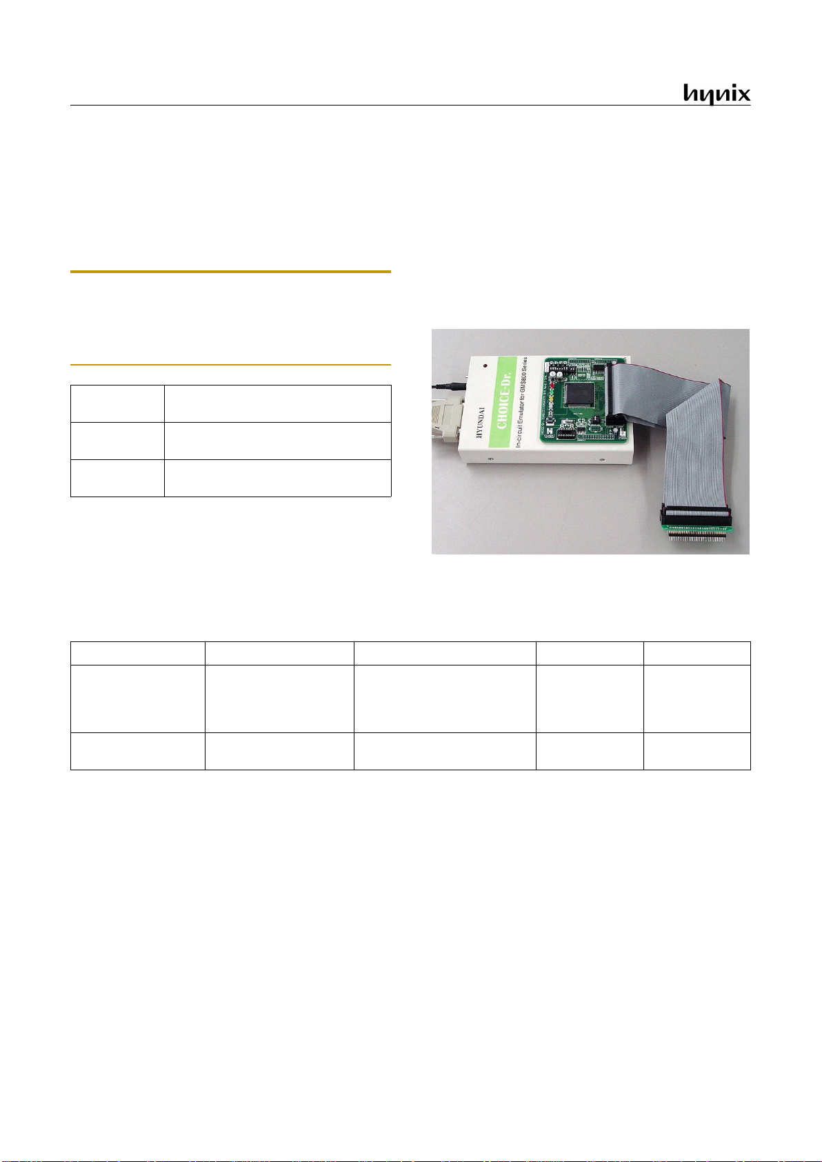
The GMS81C7008/16 is supported by a full-featured macro assembler, an in-circuit emulator CHOICE-Dr.
TM
and OTP programmers. There are two different type programmers, one is
single type, another is gang type. For more detail, refer to OTP
Programming chapt er. Ma cro as sembler ope rat es unde r the MS-
Windows 95/98TM.
Please contact sales part of Hynix semiconductor.
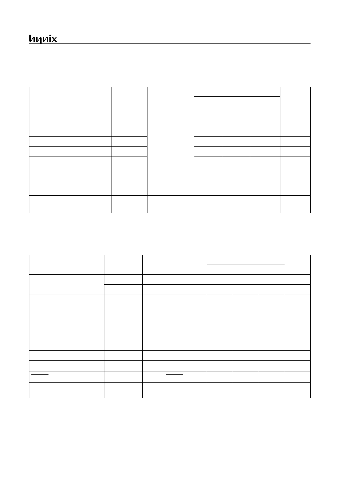
1.4 Ordering Information
Software
- MS- Window base assembler
- Linker / Editor / Debugger
Hardware
(Emulator)
- CHOICE-Dr.
- CHOICE-Dr. EVA 81C51/81C7X B/D
OTP programmer
- CHOICE-SIGMA (Single type)
- CHOICE-GANG4 (4-gang type)
Device na me ROM Size (bytes) RAM size Package
Mask ROM version
GMS81C7008 K
GMS81C7016 K
GMS81C7008 Q
GMS81C7016 Q
8K bytes
16K bytes
8K bytes
16K bytes
448 bytes
448 bytes
448 bytes
448 bytes
64SDIP
64SDIP
64MQFP
64MQFP
OTP ROM version
GMS87C7016 K
GMS87C7016 Q
16K bytes OTP
16K bytes OTP
448 bytes
448 bytes
64SDIP
64MQFP
Page 7
GMS81C7008/7016
APR., 2001 Ver 2.01 3
2. BLOCK DIAGRAM
GMS81C7008/7016
ALU
LCD Controller / Driver (LCDC)
Accumulator Stack Pointer
Interrupt Controller
Data
Memory
LCD Display
Memory
Program
Memory
Data Table
PC
8-bit Basic
Interv a l T imer
High Speed
PC
R1
R0
R3
Buzzer
Driver
PSW
System controller
Timing generator
System
Clock Controller
Clock
Generator
High freq.
Low freq.
RESET
XIN
XOUT
SXIN
SXOUT
Common Drive Output
COM0
R00 / INT0
R01 / INT1
R02 / INT2
R03 / EC0
R04 / EC2
R05 / SCK
R06 / SO
R07 / SI
R10
R11
R30 / BUZ
VDD
VSS
Power
Supply
VCL0
VCL1
VCL2
COM1/SEG26
COM2/SEG25
COM3/SEG24
LCD Power
Control Circuit
AVDD
AVSS
Power
Supply
Circuit
BIAS
R20 / AN0
R31 / PWM0 / T1O
R32 / PWM1 / T3O
R33
R21 / AN1
R22 / AN2
R23 / AN3
8-bit
A/D Converter
R2
PWM
8-bit
Timer/Counter
SIO
R24 / AN4
R25 / AN5
R26 / AN6
R27 / AN7
R4 R5 R6
R34 / WDTO
Watch/
Timer
R35 / SXOUT
R36 / SXIN
Segment Drive Output
SEG0 ~ SEG23
R40-R47
Watchdog
Key
Scan
R50-R56
R60-R67
LCD Power
Supply
Page 8
GMS81C7008/7016
4 APR., 2001 Ver 2.01
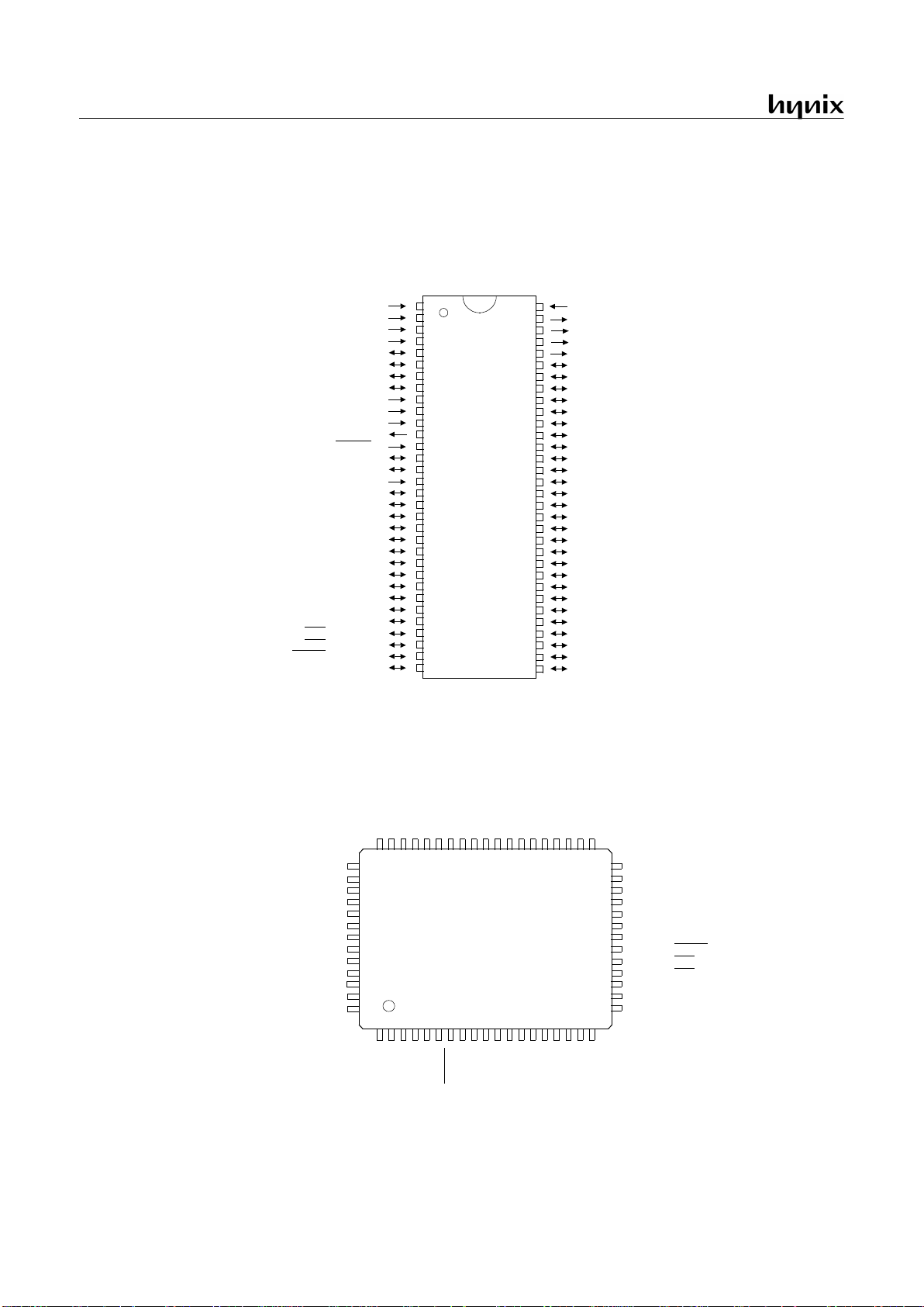
3. PIN ASSIGNMENT
VCL0
VCL1
VCL2
AV
DD
R20
R21
R22
R23
AV
SS
BIAS
X
IN
X
OUT
RESET
R36
R35
V
SS
AN0
AN1
AN2
AN3
PWM1 / T3O
PWM0 / T1O
BUZ
WDTO
R24
R25
R26
R27
R07
R06
R05
R04
R03
R02
R01
R00
R11
R10
R34
R33
SI
SO
EC2
EC0
INT2
INT1
INT0
V
DD
COM3
COM2
COM1
COM0
R67
R66
R65
R64
R63
R62
R61
R60
R57
R56
R55
R54
R53
R52
R51
R50
R47
R46
R45
R44
R43
R42
R41
R40
R30
R31
R32
R21
R66
R67
COM0
COM1
COM2
COM3
V
DD
VCL0
VCL1
VCL2
AV
DD
R20
AN1
SEG22
R02
R42
R41
R40
R30
R31
R32
R33
R34
R10
R11
R00
R01
INT2
INT0
INT1
R65
R63
R62
R61
R60
R57
R56
R55
R54
R53
R52
R51
R50
R47
R46
R45
R64
R44
R43
R22
AV
SS
BIAS
XIN
XOUT
RESET
R36
R35
VSSR24
R25
R26
R27
R07
R06
R05
R23
R04
R03
AN2
SX
IN
SX
OUT
AN4
AN5
AN6
AN7
SI
SO
SCK
AN3
EC2
EC0
123456789
101112131415161718
19
484746
45
4443424140
39
3837363534
33
515049
32
31
30
29
28
27
26
25
24
23
22
21
20
52
53
54
55
56
57
58
59
60
61
62
63
64
64MQFP
64SDIP
1
2
3
4
5
6
7
8
9
10
11
12
13
14
15
16
17
18
19
20
21
22
23
24
25
26
27
28
29
30
31
32
64
63
62
61
60
59
58
57
56
55
54
53
52
51
50
49
48
47
46
45
44
43
42
41
40
39
38
37
36
35
34
33
GMS81C7008/7016
GMS81C7008/7016
(Top View)
(Top View)
AN4
AN5
AN6
AN7
SX
IN
SX
OUT
SCK
SEG0
SEG1
SEG2
SEG3
SEG4
SEG5
SEG6
SEG7
SEG8
SEG9
SEG10
SEG11
SEG12
SEG13
SEG14
SEG15
SEG16
SEG17
SEG18
SEG19
SEG20
SEG21
SEG22
SEG23
SEG26
SEG25
SEG24
WDTO
PWM1/T3O
PWM0/T1O
BUZ
SEG0
SEG1
SEG2
SEG3
SEG4
SEG5
SEG6
SEG7
SEG8
SEG9
SEG10
SEG11
SEG12
SEG13
SEG14
SEG15
SEG16
SEG17
SEG18
SEG19
SEG20
SEG21
SEG23
AN0
SEG26
SEG25
SEG24
KS1
KS0
KS0
KS1
Page 9
GMS81C7008/7016
APR., 2001 Ver 2.01 5
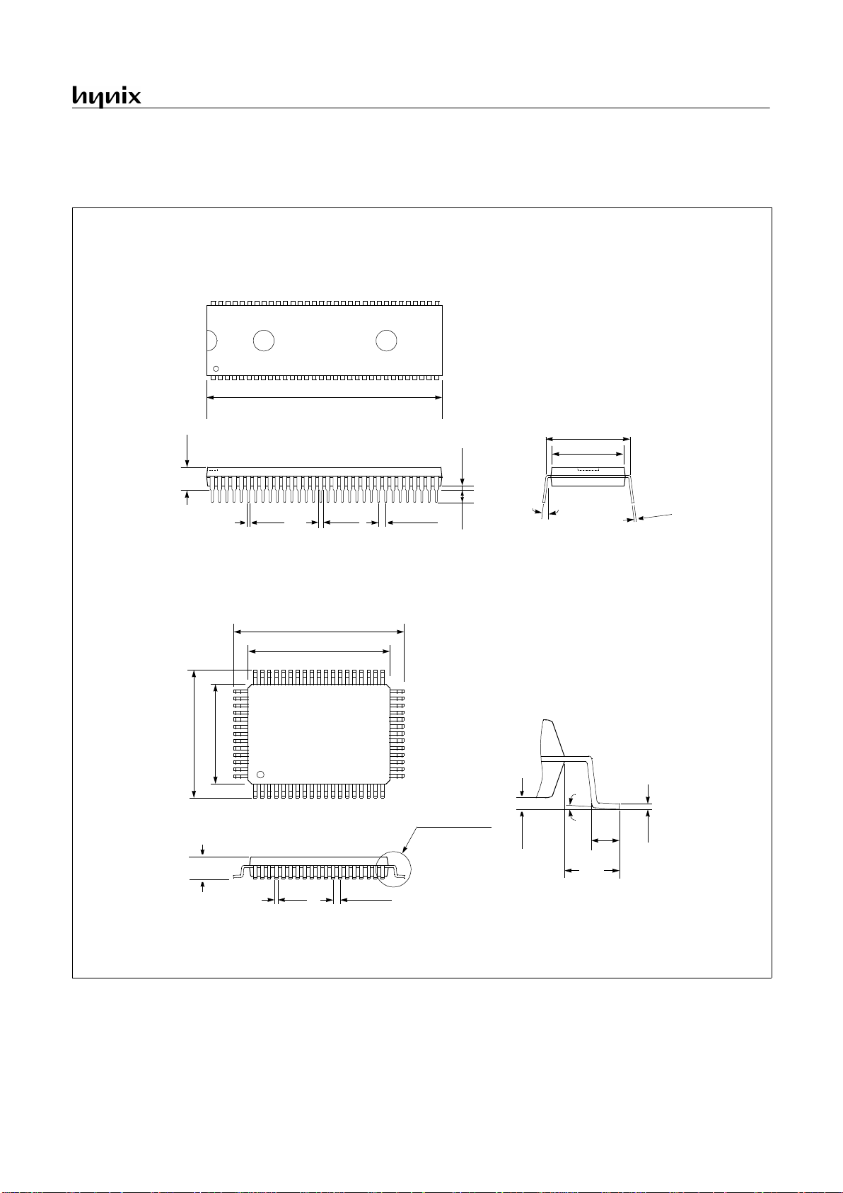
4. PACKAGE DIMENSION
UNIT: INCH
2.280
2.260
0.022
0.016
0.050
0.030
0.070 Typ.
0.140
0.120
min. 0.015
0.680
0.660
0.750 Typ.
0-15
°
64SDIP
0
.0
1
2
0
.0
0
8
0.205 max.
20.10
19.90
24.15
23.65
18.15
17.65
14.10
13.90
3.18 max.
0.50
0.35
1.00 Typ.
SEE DETAIL “A”
1.03
0.73
0-7
°
0.36
0.10
0.23
0.13
1.95
REF
DETAIL “A”
UNIT: MM
64MQFP
Page 10

GMS81C7008/7016
6 APR., 2001 Ver 2.01
5. PIN FUNCTION
V
DD
: Supply voltage.
V
SS
: Circuit ground.
RESET
: Reset the MCU.
AV
DD
: Supply voltage to the ladder resistor of ADC circuit. To
enhance the resolution of analog to digital converter, use independent powe r sour ce as we ll as po ss ibl e, oth er than digita l pow er source.
AV
SS
: ADC circuit ground.
X
IN
: Input to the in verting oscillato r amplifier a nd in put to the in-
ternal main clock operating circuit.
X
OUT
: Output from the inverting oscillator amplifier.
BIAS
: LCD bias voltage input pin.
VCL0~VCL2
: LCD driver power supply pins. The voltage on
each pin is VCL2> VCL1> VCL0. For details, Refer to “18. LCD
DRIVER” on page 70.
COM0~COM3
: LCD common signal output pins. Also, the pins
of COM1,COM2 and COM3 are shared with LCD segment signal outputs of SEG26, SEG25, SEG24 as applic ation requirement.
SX
IN
: Input to the internal subsystem clock operating circuit. In
addition, SX
IN
is shared with the R36 which is selected by the
software option.
SX
OUT
: Output from the inverting subsystem oscillator amplifi-
er. In addition, SX
OUT
is shared with the R35 which is selected
by the software option.
R00~R07:
R0 is an 8-bit CMOS bidirectio nal I/O po rt. R 0 pins 1
or 0 written to the Port Direction Register can be used as outputs
or schmitt trigger inputs. Also, pull-up resistors and open-drain
outputs are software assignable.
In addition, R0 serves the functions of the various followin g special features.
R10~R11
: R1 is a 2-bit CMOS bidirectional I/O port. R1 pins 1
or 0 written to the Port Direction Register can be used as outputs
or inputs. Also, pull-up resistors and open-drain outputs are soft-
ware assignable. These pins are not served on 81C71XX.
In addition, R0 serves t he fu n ct ion s o f th e v a riou s fo llowing sp e -
cial features.
R20~R27
: R2 is an 8-bit CMOS bidirectional I/O port. R2 p ins 1
or 0 written to the Port Direction Register can be used as outputs
or inputs. Also, pull-up resistors and open-drain outputs are software assignable.R2 4~R27 are not served on 81C71XX.
In addition, R2 is shared with the ADC input.
R30~R36
: R3 is a 7-bit CMOS bidirectional I/O port. R3 pins 1
or 0 written to the Port Direction Register can be used as outputs
or inputs. Also, pull-up resistors and open-drain outputs are software assignable. R33, R34 are not served on 81C71XX.
In addition, R3 serves the functions of the various follow ing special features.
SEG0~SEG7
: These pins generate LCD segment signal output.
Every LCD segment pins are shared with normal R4 input/output
port. R4 is an 8-bit CMOS bidirectional I/O port. R4 pins 1 or 0
written to the Port Direction Re gister can be use d as outputs or in -
Port pin Alternate function
R00
R01
R02
R03
R04
R05
R06
R07
INT0 (External interrupt 0)
INT1 (External interrupt 1)
INT2 (External interrupt 2)
EC0 (Event counter input 0)
EC2 (Event counter input 2)
SCK (Serial clock)
SO (Serial data output)
SI (Serial data input)
Port pin Alternate function
R00
R01
KS0
(Key scan 0)
KS1
(Key scan 1)
Port pin Alternate function
R20
R21
R22
R23
R24
R25
R26
R27
AN0 (Analog Input 0)
AN1 (Analog Input 1)
AN2 (Analog Input 2)
AN3 (Analog Input 3)
AN4 (Analog Input 4)
AN5 (Analog Input 5)
AN6 (Analog Input 6)
AN7 (Analog Input 7)
Port pin Alternate function
R30
R31
R32
R33
R34
R35
R36
BUZ (Buzzer driving output)
PWM0 / T1O (PWM 0 output
/ Timer 1 output)
PWM1 /T3O (PWM 1 output
/ Timer 3 output)
WDTO
(Watchdog timer output)
SX
OUT
(Sub clock output)
SX
IN
(Sub clock input)
Page 11

GMS81C7008/7016
APR., 2001 Ver 2.01 7
puts.
SEG8~SEG15
: These pins generate LCD segment signal output.
Every LCD segment pins are sh ared wit h norm al R5 in put/o utput
port. R5 is an 8-bit CMOS bidirectional I/O port. R5 pins 1 or 0
written to the Port Direction R egister can be used as outputs or in puts.
SEG16~SEG23
: These pins generate LCD segment signal output.
Every LCD segment pins are shared with normal R6 input/output
port. R6 is an 8-bit CMOS bidirectional I/O port. R6 pins 1 or 0
written to the Port Direction Re gister can be use d as outputs or in puts.
LCD pin function Port pin
SEG0 (LCD segment 0 signal output)
SEG1 (LCD segment 1 signal output)
SEG2 (LCD segment 2 signal output)
SEG3 (LCD segment 3 signal output)
SEG4 (LCD segment 4 signal output)
SEG5 (LCD segment 5 signal output)
SEG6 (LCD segment 6 signal output)
SEG7 (LCD segment 7 signal output)
R40
R41
R42
R43
R44
R45
R46
R47
LCD pin function Port pin
SEG8 (LCD segment 8 signal output)
SEG9 (LCD segment 9 signal output)
SEG10 (LCD segment 10 signal output)
SEG11 (LCD segment 11 signal output)
SEG12 (LCD segment 12 signal output)
SEG13 (LCD segment 13 signal output)
SEG14 (LCD segment 14 signal output)
SEG15 (LCD segment 15 signal output)
R50
R51
R52
R53
R54
R55
R56
R57
LCD pin function Port pin
SEG16 (LCD segment 16 signal output)
SEG17 (LCD segment 17 signal output)
SEG18 (LCD segment 18 signal output)
SEG19 (LCD segment 19 signal output)
SEG20 (LCD segment 20 signal output)
SEG21 (LCD segment 21 signal output)
SEG22 (LCD segment 22 signal output)
SEG23 (LCD segment 23 signal output)
R60
R61
R62
R63
R64
R65
R66
R67
Page 12
GMS81C7008/7016
8 APR., 2001 Ver 2.01
PIN NAME
(Alternate)
In/Out
(Alternate)
Function
Basic Alternate
V
DD
- Supply voltage
V
SS
- Circuit ground
RESET
I Reset signal input
AV
DD
- Supply voltage input pin for ADC
AV
SS
- Ground level input pin for ADC
X
IN
I Oscillation input
X
OUT
O Oscillation output
BIAS I LCD bias voltage input
VCL0~VCL2 I LCD driver power supply
COM0 O LCD common signal output
COM1(SEG26) O(O)
LCD common signal output LCD segment signal outputCOM2(SEG25) O(O)
COM3(SEG24) O(O)
R00 (INT0) I/O (I)
8-bit general I/O ports
External interrupt 0 input
R01 (INT1) I/O (I) External interrupt 1 input
R02 (INT2) I/O (I) External interrupt 2 input
R03 (EC0) I/O (I) Timer/Counter 0 external input
R04 (EC2) I/O (I) Timer/Counter 1 external input
R05 (SCK) I/O (I/O) Serial clock I/O
R06 (SO) I/O (O) Serial data output
R07 (SI) I/O (I) Serial data input
R10, R11(KS0
, KS1) I/O (I) 2-bit general I/O ports Key scan input
R20~R27(AN0~AN7) I/O(I) 8-bit general I/O ports Analog voltage input
R30(BUZ) I/O(O)
7-bit general I/O ports
Buzzer driving output
R31(PWM0 / T1O) I/O(O) PWM 0 output / Timer 1 output
R32(PWM1 / T3O) I/O(O) PWM 1 output / Timer 2 output
R33 I/O R34(WDTO
) I/O(O) Watchdog timer output
R35(SX
OUT
) I/O(O) Sub clock output
R36(SX
IN
) I/O(I) Sub clock input
SEG0 ~ SEG7
(R40~R47)
O (I/O) LCD segment signal output 8-bit general I/O ports
SEG8 ~ SEG15
(R50~R57)
O (I/O) LCD segment signal output 8-bit general I/O ports
SEG16 ~ SEG23
(R60~R67)
O (I/O) LCD segment signal output 8-bit general I/O ports
Table 5-1 Port Function Description
Page 13
GMS81C7008/7016
APR., 2001 Ver 2.01 9
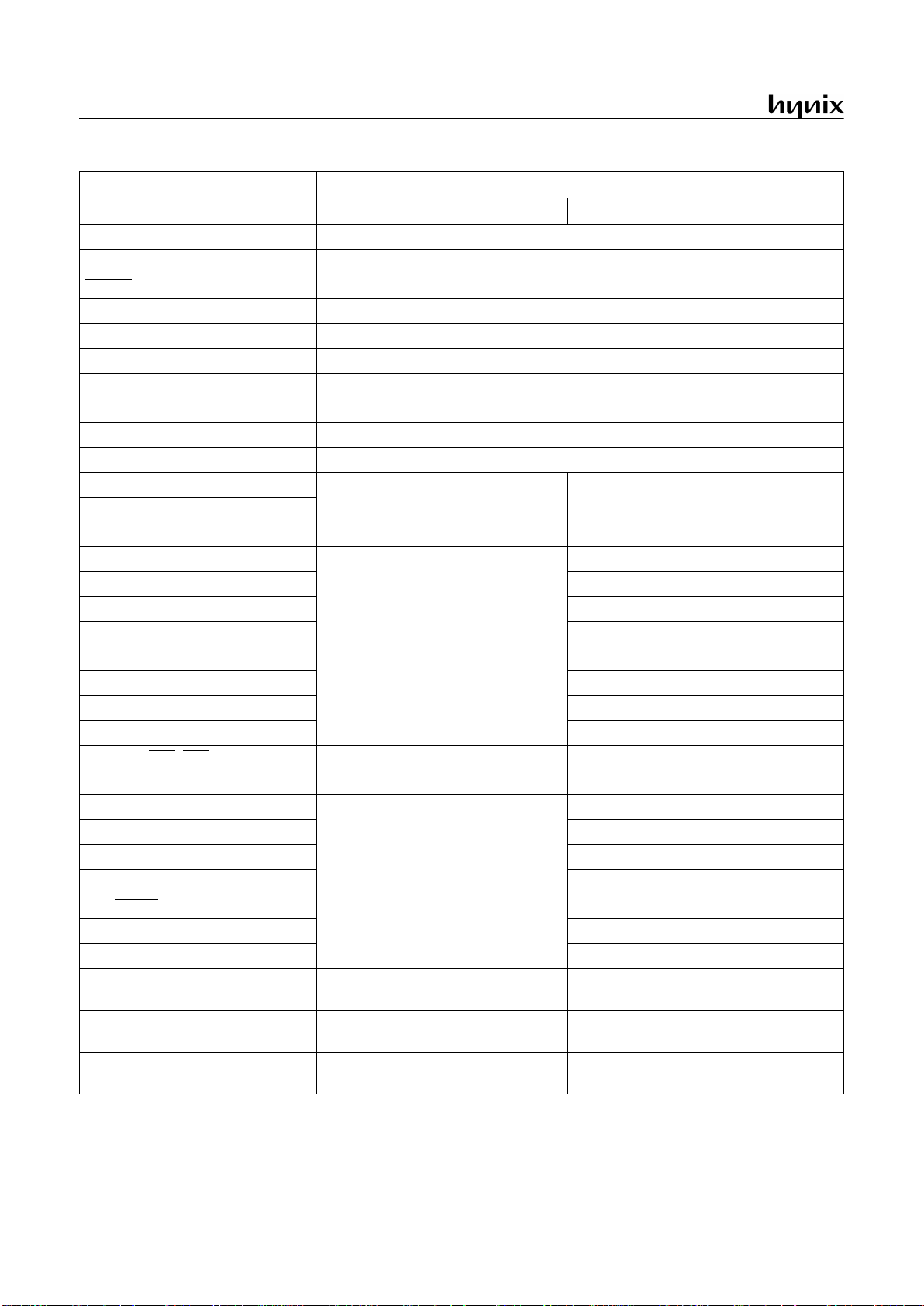
6. PORT STRUCTURES
R00/INT0, R01/INT1, R02/INT2, R03/EC0,
R04/EC2, R05/SCK, R07/S
R30/BUZ, R31/PWM0/T1O, R32/PWM1/T3O,
R34/WDTO
, R06
R20/AN0~R27/AN7
R10~R11, R33, R35, R36
RESET
SXIN, SXOUT
Pin
Data Reg.
Dir. Reg.
Noise
Canceller
INT0 ~ INT2
Pull up
Reg.
MUX
RD
V
DD
V
SS
Pull-up Tr.
EC0,EC2
Open Drain
Reg.
Data Bus
SI,SCK
Tr.: Transistor
Reg.: Register
Pin
Data Reg.
Dir. Reg.
Pull up
Reg.
MUX
V
DD
V
SS
Pull-up Tr.
Open Drain
Reg.
BUZ,SO,WDTO
Data Bus
PWM0,PWM1
RD
Pin
Data Reg.
Dir. Reg.
Analog
Switch
AN0 ~ AN7
Pull up
Reg.
MUX
RD
V
DD
V
SS
Pull-up Tr.
Open Drain
Reg.
Data Bus
Pin
Data Reg.
Dir. Reg.
Pull up
Reg.
MUX
RD
V
DD
V
SS
Pull-up Tr.
Open Drain
Reg.
Data Bus
RESET
V
SS
Noise
Canceller
Internal RESET
V
SS
V
DD
High Voltage On(OTP)
V
DD
OTP MCU :disconnected
Mask MCU :c onnected
OTP MCU :connected
Mask MCU :disconnected
SXOUT
V
SS
Internal
SXIN
Sub clock OFF
(R35)
(R36)
V
DD
System Clock
LCR.7=0
Page 14
GMS81C7008/7016
10 APR., 2001 Ver 2.01
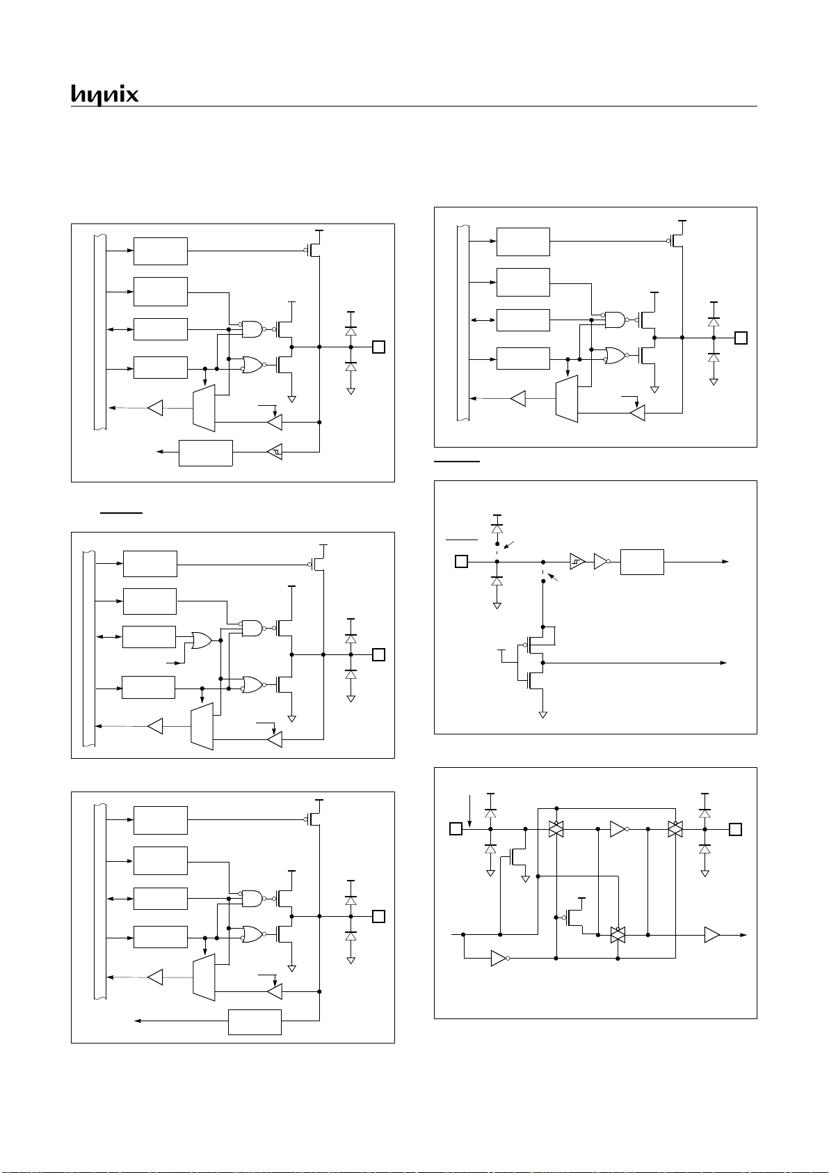
R40~R47, R50~R57, R60~R67 / SEG0~SEG23
COM0~COM3 / SEG24~SEG26
XIN, XOUT
Pin
Data Reg.
Dir. Reg.
MUX
RD
V
DD
V
SS
Data Bus
VCL2
VCL1
V
SS
VCL0
LCD Data
VCL2 Enable
LCD Data
VCL1 Enable
LCD Data
VCL0 Enable
LCD Data
GND Enable
Pin
VCL2
VCL1
V
SS
VCL0
LCD Data
VCL2 Enable
LCD Data
VCL1 Enable
LCD Data
VCL0 Enable
LCD Data
GND Enable
XOUT
V
DD
V
SS
Main Clock
XIN
STOP & Main
Clock OFF
Page 15
GMS81C7008/7016
APR., 2001 Ver 2.01 11
7. ELECTRICAL CHARACTERISTICS
7.1 Absolute Maximum Ratings
Supply voltage...........................................-0.3 to +6.0 V
Storage Temperature ................................-40 to +125 °C
Voltage on any pin with respect to Ground (V
SS
)
................................ ............................... -0.3 to V
DD
+0.3
Maximum current out of V
SS
pin........................100 mA
Maximum current into V
DD
pin ............................80 mA
Maximum current sunk by (I
OL
per I/O Pin) ........ 20 mA
Maximum output current sourced by (I
OH
per I/O Pin)
...............................................................................15 mA
Maximum current (ΣI
OL
)....................................100 mA
Maximum current (ΣI
OH
)......................................60 mA
Note: Stresses above those listed under “Absolute Maximum Ratings” may cause per manent damage to the d evice. This is a stress ra ting only and functional ope r ati on of
the device at any oth er c ond iti ons ab ov e tho se ind ic ated in
the oper ati o na l se c ti ons of this s pe c if i ca t io n i s not i mp l ie d .
Exposure to absolute maximum rating conditions for extended periods may affect device reliability.
7.2 Recommended Operating Conditions
7.3 DC Electrical Characteristics
(TA=-20~85°C, VDD=2.7~5.5V)
,
Parameter Symbol Condition
Specifications
Unit
Min. Max.
Supply Voltage
V
DD
f
XIN
=4.19MHz
f
SXIN
=32.768kHz
2.7 5.5 V
Operating Frequency
f
XIN
VDD=2.7~5.5V
14.5MHz
Sub Operating Frequency
f
SXIN
VDD=2.7~5.5V
30 35 kHz
Operating Temperature
T
OPR
-20 +85
°
C
Parameter Symbol Condition
Specifications
Unit
Min. Typ. Max.
Input High Voltage
V
IH1
RESET, R0 (except R06)
0.8 V
DD
-
V
DD
V
V
IH2
Other pins
0.7 V
DD
-
V
DD
V
Input Low Voltage
V
IL1
RESET, R0 (except R06) 0 -
0.2 V
DD
V
V
IL2
Other pins 0 -
0.3 V
DD
V
Output High Voltage
V
OH1
R0,R1,R2,R3 I
OH1
=-0.5mA
V
DD
-0.1
--V
V
OH2
SEG, COM I
OH2
=-30µA--0.4V
Output Low Voltage
V
OL1
R0,R1,R2,R3 I
OL1
=0.4mA - - 0.2 V
V
OL2
SEG, COM I
OL2
=30µA
V
DD
-0.2
--V
Input High
Leakage Current
I
IH1
VIN=V
DD
, All input pins except XIN, SX
IN
--1µA
I
IH2
VIN=V
DD, XIN
, SX
IN
--20µA
Page 16

GMS81C7008/7016
12 APR., 2001 Ver 2.01
Input Low
Leakage Current
I
IL1
VIN=0, All input pins except XIN, SX
IN
---1µA
I
IL2
VIN=0, XIN, SX
IN
- - -20
µ
A
Pull-up Resistor
1
R
PORT
VIN=0V, VDD=5.5V, R0, R1, R2 60 160 350 k
Ω
LCD Voltage Dividing
Resistor
R
LCD
VDD=5.5V 456585k
Ω
Voltage Drop
|V
DD
-COMn| , n=0~3
V
DC
VDD=2.7 ~ 5.5V
-15µA per common pin
--120mV
Voltage Drop
|V
DD
-SEGn| , n=0~26
V
DS
VDD=2.7 ~ 5.5V
-15µA per segment pin
--120mV
V
CL2
Output Voltage
V
CL2
VDD=2.7 ~ 5.5V, 1/3 bias
BIAS pin and VCL2 pin are shorted
V
DD
-0.3 V
DD
VDD+0.3
V
V
CL1
Output Voltage
V
CL1
0.66V
DD
-0.2
0.66V
DD
0.66V
DD
+0.3
V
CL0
Output Voltage
V
CL0
0.33V
DD
-0.3
0.33V
DD
0.33V
DD
+0.3
RC Oscillation Frequency
f
RC
R=60kΩ, VDD= 5V 123MHz
Supply Current
1
( ) means at 3V operation
I
DD1
Main clock operation mode
2
VDD=5.5V±10%, XIN=4MHz, S
XIN
=32kHz
-
2.9
(1.3)
7.0
(3.0)
mA
I
DD2
Sleep mode (Main active) 3
V
DD
=5.5V±10%, XIN=4MHz, S
XIN
=32kHz
-
0.4
(0.1)
1.7
(1.0)
mA
I
DD3
Stop mode
2
VDD=5V±10%, XIN= 0Hz, S
XIN
=
32kHz
2.0
(1.0)
12
(5)
µ
A
I
DD4
Sub clock operation mode
4
VDD=5.5V±10%, XIN=0Hz, S
XIN
=32kHz
-
350
(70)
500
(200)
µ
A
I
DD5
Sleep mode (Sub active)
5
VDD=3V±10%, XIN= 0Hz, S
XIN
=
32kHz
-
10
(3)
50
(20)
µ
A
I
DD6
Stop mode
4
VDD=5V±10%, XIN= 0Hz, S
XIN
=
0Hz
S
XIN
, SXOUT are used as R35, R36.
-
1.0
(0.5)
12
(5)
µ
A
1. Supply current in the following circuits are not included; on-chip pull-up resistors, internal LCD voltage dividing resistors, comparator voltage divide resistor, LVD circuit and output port drive currents.
2. This mode set System Clock Mode Register(SCMR) to xxxx0000
B
that is f
XIN
/2
3. This mode set SCMR to xxxx0000
B
(f
XIN
/2) and set SMR to “1”.
4. Main-frequency clock stops and sub-frequency clock in not used and set SCMR to xxxx0011
B
.
5. Main-frequency clock stops and sub-frequency clock in not used, set SCMR to xxxx0011
B
and set SMR to “1”.
Parameter Symbol Condition
Specifications
Unit
Min. Typ. Max.
Page 17
GMS81C7008/7016
APR., 2001 Ver 2.01 13
7.4 A/D Converter Characteristics
(TA=25°C, VSS=0V, VDD=5.0V, AVDD=5.0V @f
XIN
=4MHz)
7.5 AC Characteristics
(TA=-20~+85°C, VDD=5V±10%, VSS=0V)
Parameter Symbol Test Condition
Specifications
Unit
Min.
Typ.
1
1. Data in “Typ” column is at 25°C unless otherwise stated. These parameters are for design guidance only and are not tested.
Max.
Analog Input Voltage Range
V
AIN
VDD=AVDD=5.0V
V
SS
-0.3
-
AVDD+0.3
V
Non-linearity Error
N
NLE
-
±
1.0 ±1.5 LSB
Differential Non-linearity Error
N
DNLE
-
±
1.0 ±1.5 LSB
Zero Offset Error
N
ZOE
-
±
0.5 ±1.5 LSB
Full Scale Error
N
FSE
-
±
0.25 ±0.5 LSB
Gain Error
N
GE
-
±
1.0 ±1.5 LSB
Overall Accuracy
N
ACC
-
±
1.0 ±1.5 LSB
AV
DD
Input Current
I
REF
- - 200
µ
A
Conversion Time
T
CONV
--20µs
Analog Power Supply Input Range
AV
DD
VDD=5.0V
V
DD
=3.0V
3.0
2.7
-
V
DD
V
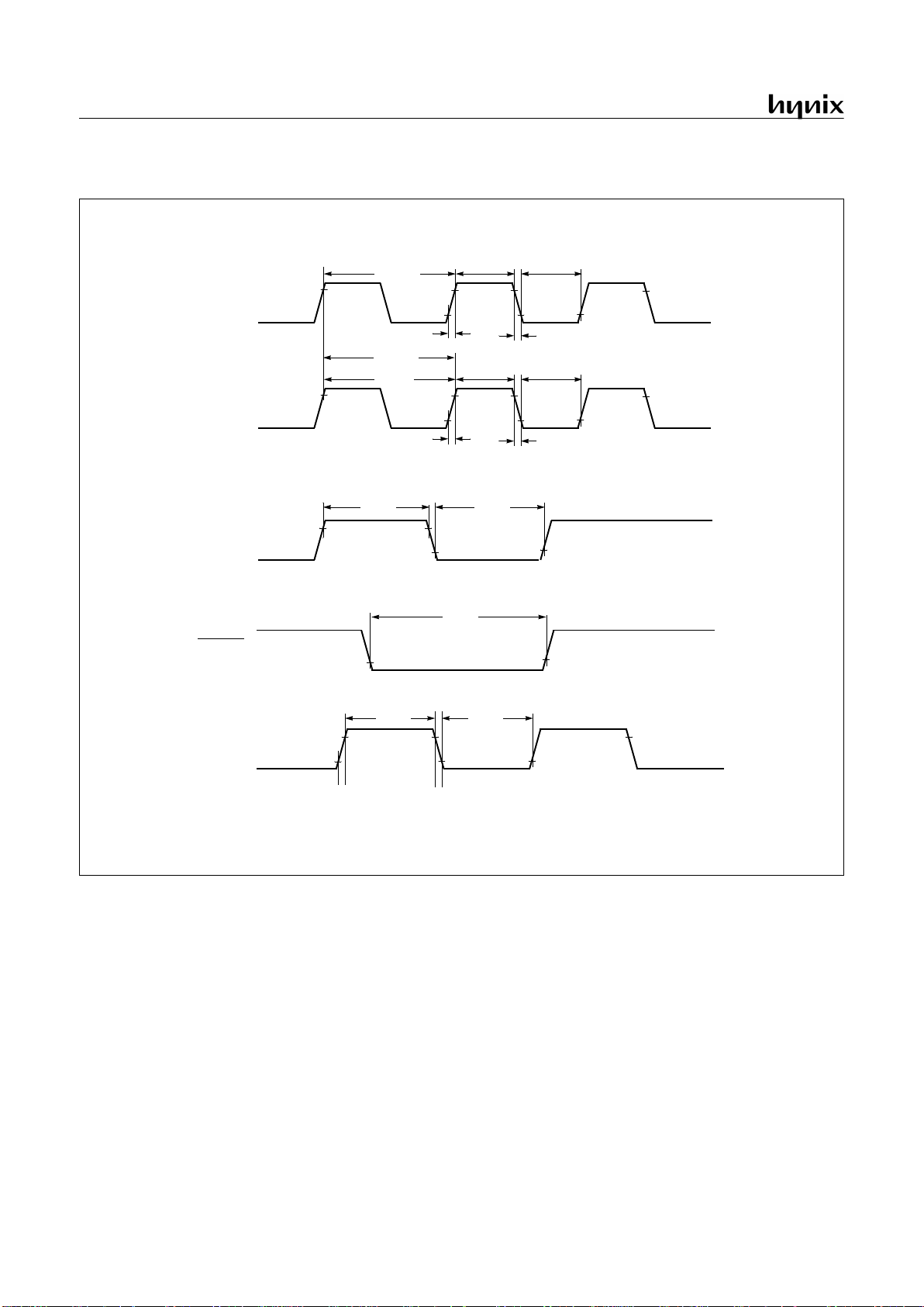
Parameter Symbol Pins
Specifications
Unit
Min. Typ. Max.
Operating Frequency
f
MAIN
X
IN
0.455 - 4.2 MHz
f
SUB
SX
IN
30 32.768 35 kHz
External Clock Pulse W idth
t
MCPW
X
IN
80 - - nS
t
SCPW
SX
IN
14.7 - -
µ
S
External Clock Transition Time
t
MRCP,tMFCP
X
IN
- - 20 nS
t
SRCP,tSFCP
SX
IN
--3µS
Main oscillation Stabilizing
Time
t
MST
XIN, X
OUT
at 4MHz
--20mS
Sub oscillation Stabilizing Time
t
SST
SXIN, SX
OUT
-0.51 S
Interrupt Pulse Width
t
IW
INT0, INT1, INT2 2 - -
t
SYS
1
RESET Input Width
t
RST
RESET 8--t
SYS
1
Event Counter Input Pulse
Width
t
ECW
EC0, EC2 2 - -
t
SYS
1
1. t
SYS
is one of 2/f
MAIN
or 8/f
MAIN
or 16/f
MAIN
or 64/f
MAIN
in the main clock operation mode,
t
SYS
is one of 2/f
SUB
or 8/f
SUB
or 16/f
SUB
or 64/f
SUB
in the sub clock operation mode.
Page 18
GMS81C7008/7016
14 APR., 2001 Ver 2.01
Figure 7-1 Timing Chart
t
MRCP
t
MFCP
X
IN
INT0, INT1
INT2
0.5V
V
DD
-0.5V
0.2V
DD
0.8V
DD
0.2V
DD
RESET
0.2V
DD
0.8V
DD
EC0, EC2
t
IW
t
IW
t
RST
t
ECW
t
ECW
1/f
MAIN
t
MCPW
t
MCPW
t
SRCP
t
SFCP
SX
IN
0.5V
V
DD
-0.5V
1/f
SUB
t
SCPW
t
SCPW
t
SYS
Page 19
GMS81C7008/7016
APR., 2001 Ver 2.01 15
7.6 Serial Interface Timing Characteristics
(TA=-20~+85°C, VDD=2.7~5.5V, VSS=0V, f
XIN
=4MHz)
Figure 7-2 Serial I/O Timing Chart
Parameter Symbol Pins
Specifications
Unit
Min. Typ. Max.
Serial Input Clock Pulse
t
SCYC
SCK
2t
SYS
+200
-8ns
Serial Input Clock Pulse Width
t
SCKW
SCK
t
SYS
+70
-8ns
SIN Input Setup Time (External SCK)
t
SUS
SIN 100 - - ns
SIN Input Setup Time (Internal SCK)
t
SUS
SIN 200 - - ns
SIN Input Hold Time
t
HS
SIN
t
SYS
+70
--ns
Serial Output Clock Cycle Time
t
SCYC
SCK
4t
SYS
-
16t
SYS
ns
Serial Output Clock Pulse Width
t
SCKW
SCK
t
SYS
-30
--ns
Serial Output Clock Pulse Transition
Time
t
FSCK
t
RSCK
SCK - - 30 ns
Serial Output Delay Time
s
OUT
SO - - 100 ns
SCLK
SIN
0.2V
DD
SOUT
0.2V
DD
0.8V
DD
t
SCYC
t
SCKW
t
SCKW
t
RSCK
t
FSCK
0.8V
DD
t
SUS
t
HS
t
DS
0.2V
DD
0.8V
DD
Page 20
GMS81C7008/7016
16 APR., 2001 Ver 2.01
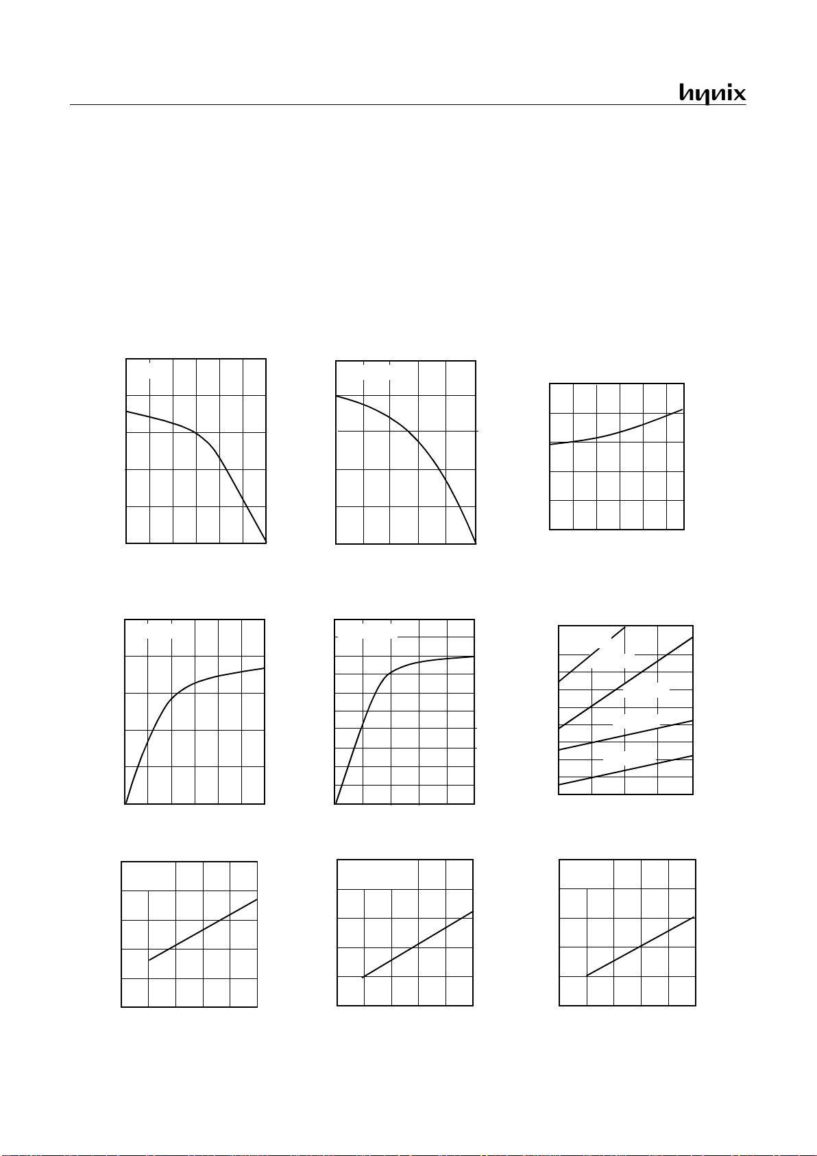
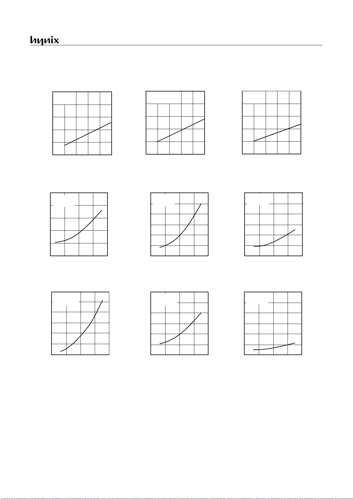
7.7 Typical Characteristics
This graphs and tables provided in this section are for design guidance only and are not tested or guaranteed.
In some graphs or tables the data presented are outside specified operating range (e.g. outside specified
VDD range). This is for information only and devices
are guaranteed to operate properly only within the
specified range.
The data presented in this s ection is a statistical s ummary
of data collected on units from different lots over a period
of time. “Typical” represents the mean of the distribution
while “max” or “min” represents (mean + 3σ) and (mean
−
3σ) respectively where σ is standard deviation
I
OL
−−−−
V
OL
, VDD=5.5V
40
30
20
10
0
(mA)
I
OL
V
OL
(V)
I
OL
−−−−
V
OL
, VDD=3.0V
(mA)
I
OL
0.5 1.0 1.5 2.0 2.5
V
OL
(V)
I
OH
−−−−
V
OH
, VDD=5.0V
-20
-15
-10
-5
0
(mA)
I
OH
12345
V
OH
(V)
I
OH
−−−−
V
OH
, VDD=3.0V
-8
-6
-4
-2
0
(mA)
I
OH
0.5 1.0 1.5 2.0 2.5
V
OH
(V)
Ta=25°C
R0,R1,R2,R3 pin
200
100
0
(kΩ)
-20
04080
Ta
(°C)
R
12345
f
XIN
=4MHz
V
DD
−−−−
V
IH1
4
3
2
1
0
(V)
V
IH1
23
45
6
V
DD
(V)
V
DD
−−−−
V
IH2
4
3
2
1
0
(V)
V
IH2
23
45
6
V
DD
(V)
Ta=25°C
f
XIN
=4MHz
Ta=25°C
1
R0 (except R06)
R1~R6 pin
20
15
10
5
(include R06)
f
XIN
=4MHz
V
DD
−−−−
V
IH3
4
3
2
1
0
(V)
V
IH1
23
45
6
V
DD
(V)
Ta=25°C
1
XIN, SX
IN
R = 6.2k
Ω
4
3
2
1
0
(MHz)
f
XIN
2345
6
V
DD
(V)
Ta=25°C
R = 20k
Ω
R = 180k
Ω
R = 60k
Ω
f
XIN
−−−−
V
DD
Ta=25°C
Ta=25°CTa=25°C
R
PU
−−−−
T
a
, VDD=5.0V
Page 21
GMS81C7008/7016
APR., 2001 Ver 2.01 17
I
STOP
((((
I
DD6
)
−−−−
V
DD
STOP Mode
I
DD1
−−−−
V
DD
4
3
2
1
0
(mA)
I
DD
6
V
DD
(V)
Normal Operation (Main opr.)
I
DD4
−−−−
V
DD
400
300
200
100
0
(µA)
I
DD
23
45
6
V
DD
(V)
Normal Mode (Sub opr.)
I
SLEEP(IDD5
)
−−−−
V
DD
SLEEP Mode (Sub opr.)
I
SLEEP(IDD2
)
−−−−
V
DD
f
XIN
=4MHz
V
DD
−−−−
V
IL1
4
3
2
1
0
(V)
V
IH1
23
45
6
V
DD
(V)
V
DD
−−−−
V
IL2
4
3
2
1
0
(V)
V
IH2
23
45
6
V
DD
(V)
Ta=25°C
f
XIN
=4MHz
Ta=25°C
1
R0 (except R06)
R1~R6 pin
(include R06)
f
XIN
=4MHz
V
DD
−−−−
V
IL3
4
3
2
1
0
(V)
V
IH1
23
45
6
V
DD
(V)
Ta=25°C
1
XIN, SX
IN
23
45
SLEEP Mode (Main opr.)
f
SXIN
=32kHz
Ta=25°C
400
300
200
100
0
(µA)
I
DD
23
45
6
V
DD
(V)
12
9
6
3
0
(µA)
I
DD
23
45
6
V
DD
(V)
f
SXIN
=32kHz
Ta=25°C
I
STOP(IDD3
)
−−−−
V
DD
STOP Mode
4
3
2
1
0
(µA)
I
DD
23
45
6
V
DD
(V)
f
XIN
=0Hz
Ta=25°C
f
XIN
=4MHz
Ta=25°C
f
XIN
=4MHz
Ta=25°C
4
3
2
1
0
(µA)
I
DD
23
45
6
V
DD
(V)
f
SXIN
=0Hz
Ta=25°C
Page 22
GMS81C7008/7016
18 APR., 2001 Ver 2.01
8. MEMORY ORGANIZATION
The GMS81C7008/16 has separate address spaces for Program
memory and Data Memory. Program memory can only be read,
not written to. It can be u p to 8 K/16 K b yt es of Pro gram me m ory.
Data memory can be read and written to up to 448 bytes including
the stack area and the LCD display RAM area.
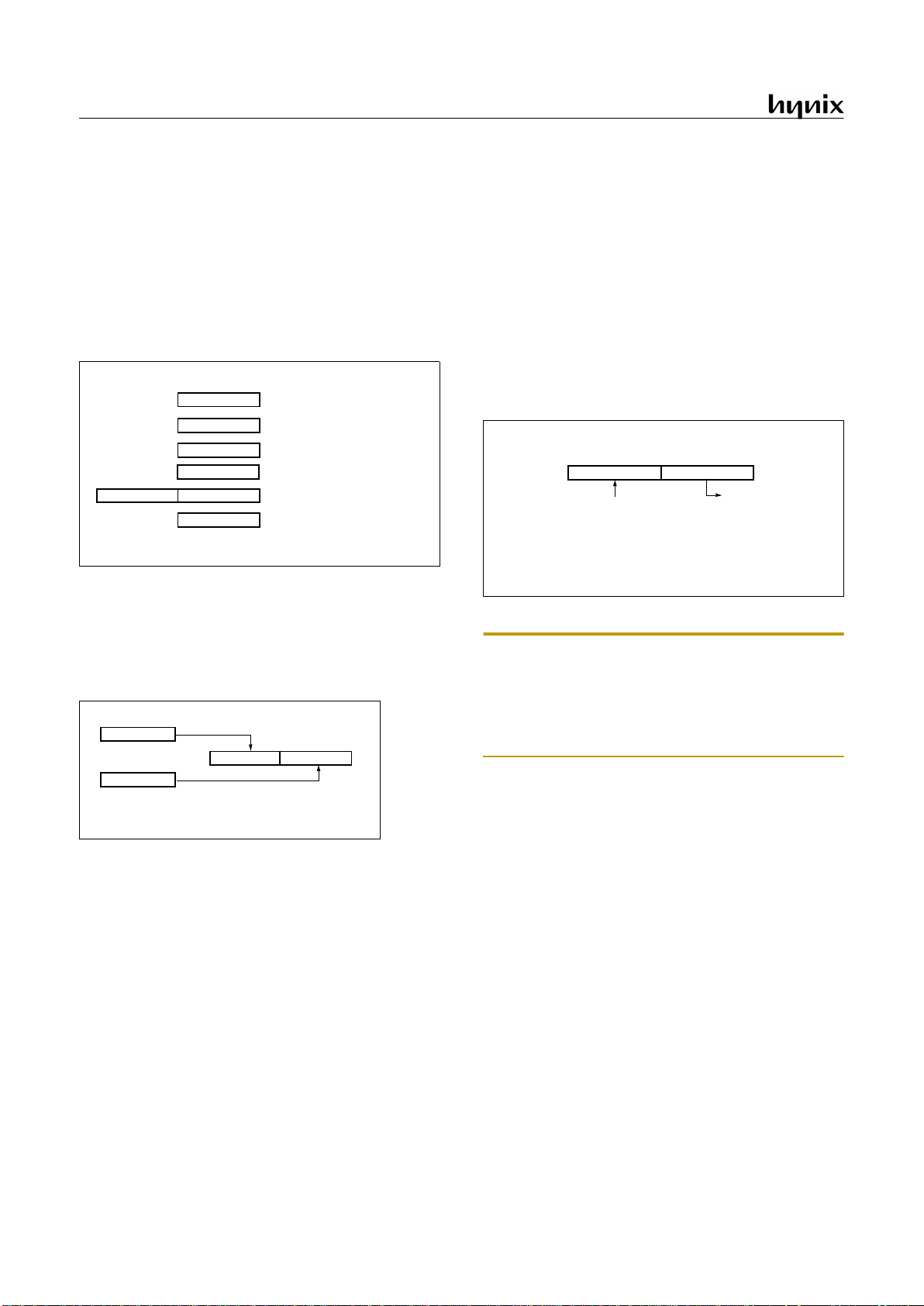
8.1 Registers
This device has six registers that are the Program Counter (PC),
a Accumulator (A), two index registers (X, Y), the Stack Pointer
(SP), and the Program Status Word (PSW). The Program Counter
consists of 16-bit register.
Figure 8-1 Configuration of Registers
Accumulator:
The Accumulator is the 8-bit general purpose register, used for data operat ion such as transfe r, tempor ary sav ing,
and conditional judgement, etc.
The Accumulator can be used as a 1 6-bit register with Y Register
as shown below.
Figure 8-2 Configuration of YA 16-bit Register
X, Y Registers
: In the addressing mode which uses these index
registers, the register contents are adde d to the specified address,
which becomes the actual address. These modes are extremely effective for referencing subroutine tables and memory tables. The
index registers also hav e incremen t, decremen t, compari son and
data transfer functions, and they can be used as simple accumulators.
Stack Pointer
: The Stack Pointer is an 8-bit register used for occurrence interrupts and calling out subroutines. Stack Pointer
identifies the location in the stack to be access (save or restore).
Generally, SP is automatically updated when a subroutine call is
executed or an interrupt is accepted. However, if it is used in ex-
cess of the stack area permitted by the data memory allocating
configuration, the user-processed data may be lost.
The stack can be located at any po sit ion wit hin 01 1B
H
to 01FF
H
of the internal data memory. The SP is not initialized by hardware, requiring to write the initial value (the location with which
the use of the stack starts) by using the initializ ation routin e. Normally, the initial value of “FF
H
” is used.
Note: The Stack Pointer must be initialized by software because its value is undefined after RESET.
Example: To initialize the SP
LDX #0FFH
TXSP ; SP ← FFH
Program Counter
: The Program Counter is a 16-bit wide which
consists of t wo 8-b it regi sters, P CH an d PC L. Thi s co un ter ind icates the address of the next in struction to be execut ed. In reset
state, the program counter has reset routine address (PC
H
:0FFH,
PC
L
:0FEH).
Program Status Word
: The Program Status Word (PSW) contains several bits that reflect the current state of the CPU. The
PSW is described in Figure 8-3. It contains the Negative flag, the
Overflow flag, the Break flag the Half Carry (for BCD operation), the Interrupt enable flag, the Zero flag, and the Carry flag.
[Carry flag C]
This flag stores any carry or not borrow from the ALU of CPU
after an arithmetic operation and is also changed by the Shift Instruction or Rotate Instruction.
[Zero flag Z]
This flag is set when the result of an arithmetic operation or data
transfer is “0” and is cleared by any other result.
ACCUMULATOR
X REGISTER
Y REGISTER
STACK POINTER
PROGRAM COUNTER
PROGRAM STATUS
WORD
X
A
SP
Y
PCL
PSW
PCH
Two 8-bit Registers can be used as a “YA” 16-bit Register
Y
A
Y A
SP
01
H
Stack Area (100H ~ 1FFH)
Bit 15 Bit 087
Hardware fixed
00H~FF
H
LCD display RAM area is located in 100H~11AH,
SP (Stack Pointer) could be in 00
H
~FFH.
User must have concerning that Stack data does not
cross over LCD RAM area.
Page 23
GMS81C7008/7016
APR., 2001 Ver 2.01 19
Figure 8-3 PSW (Program Status Word) Register
[Interrupt disable flag I]
This flag enables/disables all interrupts except interrupt caused
by Reset or software BRK instruction. All interrupts are disabled
when cleared to “0”. This flag immediately becomes “0” when an
interrupt is served. It i s set by the EI instruction and cleared by
the DI instruction.
[Half carry flag H]
After operation, this is set when there is a carry from bit 3 of ALU
or there is no borrow from bit 4 of ALU. This bit can not be set
or cleared except CLRV instruction with Overflow flag (V).
[Break flag B]
This flag is set by software BRK instruction to distinguish BRK
from TCALL instruction with the same vector address.
[Direct page flag G]
This flag assigns RAM page for direct addressing mode. In the d i-
rect addressing mode, addressing area is from zero page 00
H
to
0FF
H
when this flag is "0". If it is set to "1", addressing area is
assigned by RPR register (address 0F3
H
). It is set by SETG in-
struction and clear ed by CLRG.
When content of RPR is above 2, malfunction will be occurred.
[Overflow flag V]
This flag is set to “1” when an overflow occurs as the result of an
arithmetic operation involving signs. An overflow occurs when
the result of an addition or subtraction exceeds +127(7FH) or 128(80
H
). The CLRV instruction clears the overflow flag. There
is no set instruction. When the BIT instruction is executed, bit 6
of memory is copied to this flag.
[Negative flag N]
This flag is set to match the sign bit (bit 7) status of the result of
a data or arithmetic operation. When the BIT instruction is executed, bit 7 of memory is copied to this flag.
N
NEGATIVE FLAG
V G B H I Z C
MSB LSB
RESET VALUE: 00
H
PSW
OVERFLOW FLAG
BRK FLAG
CARRY FLAG RECEIVES
ZERO FLAG
INTERRUPT ENABLE FLAG
CARRY OUT
HALF CARRY FLAG RECEIVES
CARRY OUT FROM BIT 1 OF
ADDITION OPERLANDS
SELECT DIRECT PAGE
when G=1, page is selected to “page 1”
RAM Page Instruction
Bit1 of
RPR
Bit0 of
RPR
0 page CLRG X X
0 page SETG 0 0
1 page SETG 0 1
Reserved SETG 1 0
Reserved SETG 1 1
Page 24
GMS81C7008/7016
20 APR., 2001 Ver 2.01
Figure 8-4 Stack Operation
At execution of
a CALL/TCALL/PCALL
PCL
PCH
01FC
SP after
execution
SP before
execution
01FD
01FD
01FE
01FF
01FF
Push
down
At acceptance
of interrupt
PCL
PCH
01FC
01FC
01FD
01FE
01FF
01FF
Push
down
PSW
At execution
of RET instruction
PCL
PCH
01FC
01FF
01FD
01FE
01FF
01FD
Pop
up
At execution
of RET instruction
PCL
PCH
01FC
01FF
01FE
01FE
01FF
01FC
Pop
up
PSW
0100H
01FFH
Stack
depth
At execution
of PUSH instruction
A
01FC
01FE
01FD
01FE
01FF
01FF
Push
down
SP after
execution
SP before
execution
PUSH A (X,Y,PSW)
At execution
of POP instruction
A
01FC
01FF
01FD
01FE
01FF
01FE
Pop
up
POP A (X,Y,PSW)
Page 25
GMS81C7008/7016
APR., 2001 Ver 2.01 21
8.2 Program Memory
A 16-bit program counter is capable of addressing up to 64K
bytes, but this device has 8K/16K bytes program memory space
only physically implemented. Accessing a location above FFFF
H
will cause a wrap-around to 0000H.
Figure 8-5, shows a map of Program Memory. After reset, the
CPU begins execution from reset vector which is stored in address FFFE
H
and FFFFH as shown in Figure 8-6.
As shown in Figure 8-5, each area is assigned a fixed location i n
Program Memory. Prog ram Me mory ar ea co ntain s the u ser p rogram.
Figure 8-5 Program Memory Map
Page Call (PCALL) area contains subroutine program to reduce
program byte lengt h by usi ng 2 bytes PCALL inst ead of 3 by tes
CALL instruction. If it is frequently called, it is more useful to
save program byte length.
Table Call (TCALL) causes the CPU to jump to each TCALL ad-
dress, where it commences the execution of the service routine.
The Table Call service area spaces 2-byte for every TCALL:
0FFC0H for TCALL15, 0FFC2H for TCALL14, etc., as shown in
Figure 8-7.
Example: Usage of TCALL
The interrupt causes the CPU to jump to specific locati on, whe re
it commences the execution of the service routine. The External
interrupt 0, for example, is assigned to location 0FFFA
H
. The in-
terrupt service locations spaces 2-byte interval: 0FFF8
H
and
0FFF9
H
for External Interrupt 1, 0FFFAH and 0FFFBH for Exter-
nal Interrupt 0, etc.
Any area from 0FF00H to 0FFFFH, if it is not going to be used,
its service location is availab le as general p urpose Program Memory.
Figure 8-6 Interrupt Vector Area
Interrupt
Vector Area
C000
H
FEFF
H
FF00
H
FFC0
H
FFDF
H
FFE0
H
FFFF
H
PCALL area
E000
H
TCALL area
GMS81C7008
8K ROM
GMS81C7016
16K ROM
0FFE0
H
E2
Address Vector Area Memory
E4
E6
E8
EA
EC
EE
F0
F2
F4
F6
F8
FA
FC
FE
Timer/Counter 3
Timer/Counter 2
Watch Timer
A/D Converter
-
External Interrupt 0
Timer/Counter 1
Basic Interval Timer
Key Scan
RESET
Watchdog Timer
Serial Peripheral Interface
“-” means reserved area.
NOTE:
External Interrupt 2
External Interrupt 1
Timer/Counter 0
-
-
Page 26
GMS81C7008/7016
22 APR., 2001 Ver 2.01
Figure 8-7 PCALL and TCALL Memory Area
PCALL
→
→ →
→
rel
4F35 PCALL 35H
TCALL
→
→ →
→
n
4A TCALL 4
0FFC0
H
C1
Address Program Memory
C2
C3
C4
C5
C6
C7
C8
0FF00
H
Address
PCALL Area Memory
0FFFF
H
PCALL Area
(256 Bytes)
* means that the BRK software interrupt is using
same address with TCALL0.
NOTE:
TCALL 15
TCALL 14
TCALL 13
TCALL 12
TCALL 11
TCALL 10
TCALL 9
TCALL 8
TCALL 7
TCALL 6
TCALL 5
TCALL 4
TCALL 3
TCALL 2
TCALL 1
TCALL 0 / BRK *
C9
CA
CB
CC
CD
CE
CF
D0
D1
D2
D3
D4
D5
D6
D7
D8
D9
DA
DB
DC
DD
DE
DF
4F
~
~
~
~
NEXT
35
0FF35
H
0FF00
H
0FFFF
H
11111111 11010110
01001010
PC:
FH FH DH 6H
4A
~
~
~
~
25
0FFD6
H
0FF00
H
0FFFF
H
D1
NEXT
0FFD7
H
0D125
H
Reverse
1
2
3
Page 27

GMS81C7008/7016
APR., 2001 Ver 2.01 23
Example: The usage software example of Vector address for GMS81C7016.
ORG 0FFE0H
DW TIMER3 ; Timer-3
DW TIMER2 ; Timer-2
DW WATCH_TIM ER ; Watch Timer
DW ADC ; ADC
DW SIO ; Serial Interface
DW NOT_USED ; DW NOT_USED ; DW INT2 ; Int.2
DW TIMER1 ; Timer-1
DW TIMER0 ; Timer-0
DW INT1 ; Int.1
DW INT0 ; Int.0
DW WD_TIMER ; Watchdog Timer
DW BIT_TIMER ; Basic Interval Timer
DW KEYSCAN ; Key Scan Timer
DW RESET ; Reset
ORG 0C000H ; in case of 16K ROM Start address
; ORG 0E000H ; in case of 8K ROM Start address
;*******************************************
; MAIN PROGRAM *
;*******************************************
;
RESET: LDM SCMR,#0 ;When main clock mode
DI ;Disable All Interrupts
LDM WDTR,#0 ;Disable Watch Dog Timer
LDM RPR,#1
CLRG
LDX #0
RAM_CLR: LDA #0 ;RAM Clear(!0000H ~ !00BFH)
STA {X}+
CMPX #0C0H
BNE RAM_CLR
SETG
LDX #0
RAM_CLR1:
LDA #0
STA {X}+
CMPX #1BH ;DISPLAY RAM Clear(!0100H ~ !011AH)
BNE RAM_CLR1
CLRG
;
LDX #0FFH ;Stack Pointer Initialize
TXSP
;
LDM R0, #0 ;Normal Port 0
LDM R0DD,#82H ;Normal Port Direction
LDM R0PU,#0 ;Normal Pull Up
:
:
:
LDM TDR0,#250 ;8us x 250 = 2000us
LDM TM0,#0000_1111B ;Start Timer0, 8us at 4MHz
LDM IRQH,#0
LDM IRQL,#0
LDM IENH,#0000_1110B ;Enable INT0, INT1, Timer0
LDM IENL,#0
LDM IEDS,#15H ;Select falling edge detect on INT pin
LDM PMR,#3H ;Set external interrupt pin(INT0, INT1)
EI ;Enable master interrupt
Page 28
GMS81C7008/7016
24 APR., 2001 Ver 2.01
8.3 Data Memory
Figure 8-8 shows the internal Data Memory space available. Data
Memory is divided into f our g roups, a user RA M, cont rol registers, Stack, and LCD memory.
Figure 8-8 Data Memory Map
User Memory
The both GMS81C7008/16 has 448 × 8 bits for the user memory
(RAM).
There are two page internal RAM. Page is selected by G-flag and
RAM page selection register RPR. When G-flag is cleared to “0”,
always page 0 is selected regardless of RPR value. If G-flag is set
to “1”, page will be selected ac cording to RPR value.
Figure 8-9 RAM page configuration
Control Registers
The control registers are used by the CPU and Peripheral function
blocks for controlling the desired operation of the device. T herefore these registers contain control and status bits for the interrupt
system, the timer/ counters, anal og to digital con verters and I/O
ports. The control registers are in address range of 0C0
H
to 0FFH.
Note that unoccupi ed addres ses may not be implem ented o n the
chip. Read accesses to these addresses will in general return random data, and write accesses will have an indeterminate effect.
More detailed informations of each register are explained in each
peripheral section.
Note: Write only registers can not be accessed by bit manipulation instruction (SET 1, CLR1 ). Do not use read-modify-write instruction. Use byte manipulation instruction, for
example “LDM”.
Example; To write at CKCTLR
LDM CKCTLR,#09H
;Divide ratio(÷16)
Stack Area
The stack p r ov i d es t h e area where the return address is sav ed before a jump is performed during the processing routine at th e execution of a subroutine call instruction or the acceptance of an
interrupt.
When returning from the processing routine, executing the subroutine return instruction [RET] restores the contents of the program counter from the stack; executing the interrupt return
instruction [RETI] restores the contents of the program counter
and flags.
The save/restore locations in the stack are determined by the
stack pointed (SP). The SP is automatically decreased after the
saving, and increased before the restoring. This means the value
of the SP indicates the stack location number for the next save.
Refer to Figure 8-4 on page 20.
User Memory
Control
Registers
or Stack Area
0000
H
00BF
H
00C0
H
00FF
H
0100
H
01FF
H
PAGE0
User Memory
PAGE1
LCD display RAM
(27 Nibbles)
011A
H
011B
H
(192 Bytes)
(229 Bytes)
Page 0
Page 0: 00~FF
H
Page 1
Page 1: 100~1FF
H
RPR=1, G=1
G=0
Page 29
GMS81C7008/7016
APR., 2001 Ver 2.01 25
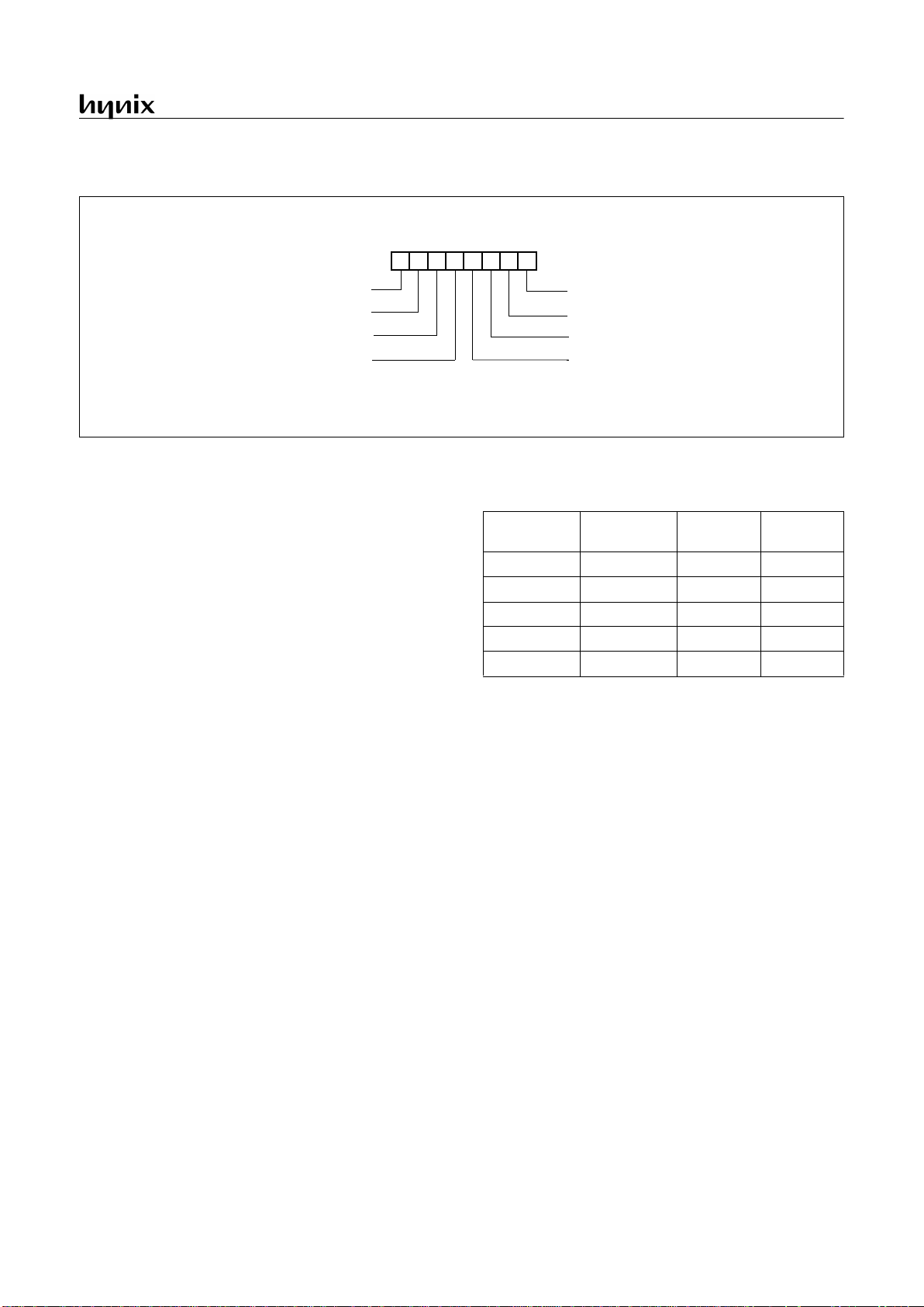
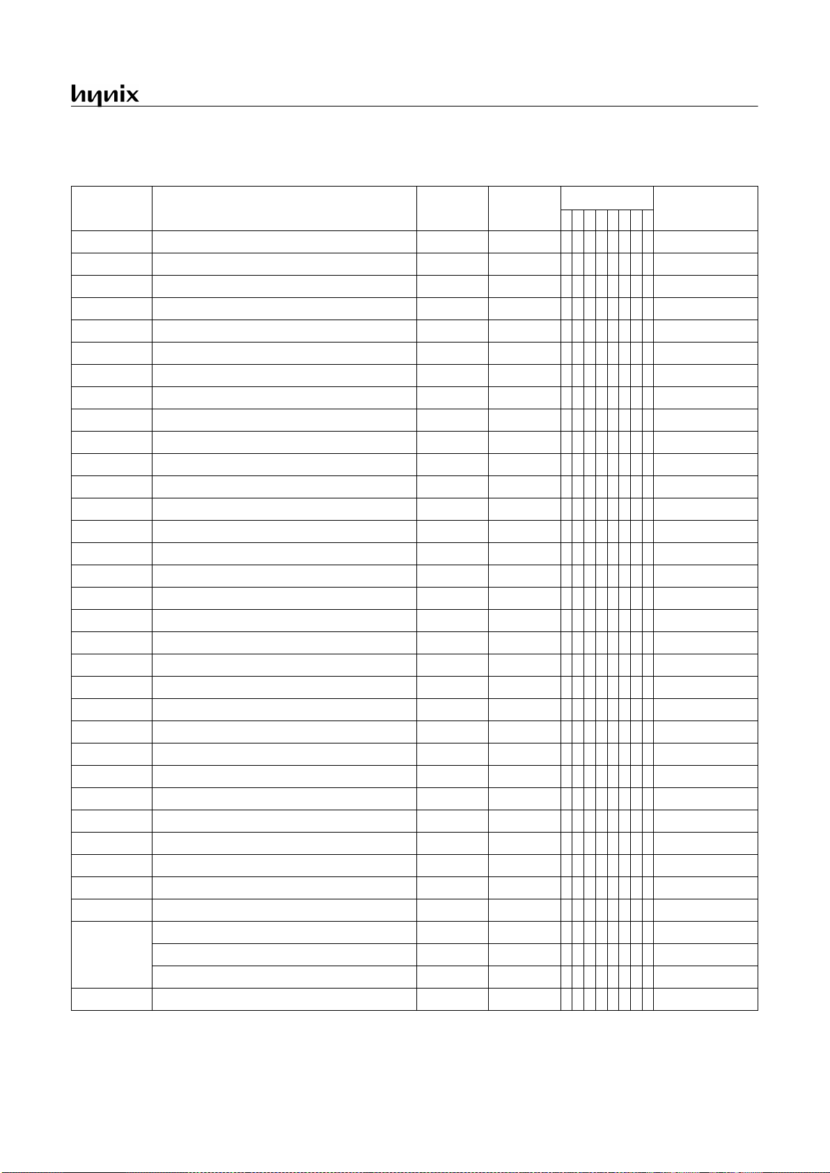
8.4 List of Control Registers
Address Register Name Symbol R/W
Initial Value
Page
76543210
00C0 R0 port data register R0 R/W 0 0 0 0 0 0 0 0 page 33
00C1 R1 port data register R1 R/W - - - - - - 0 0 page 33
00C2 R2 port data register R2 R/W 0 0 0 0 0 0 0 0 page 33
00C3 R3 port data register R3 R/W - 0 0 0 0 0 0 0 page 33
00C4 R4 port data register R4 R/W 0 0 0 0 0 0 0 0 page 34
00C5 R5 port data register R5 R/W 0 0 0 0 0 0 0 0 page 34
00C6 R6 port data register R6 R/W 0 0 0 0 0 0 0 0 page 35
00C8 R0 port I/O direction register R0DD W 0 0 0 0 0 0 0 0 page 35
00C9 R1 port I/O direction register R1DD W - - - - - - 0 0 page36
00CA R2 port I/O direction register R2DD W 0 0 0 0 0 0 0 0 page 36
00CB R3 port I/O direction register R3DD W - 0 0 0 0 0 0 0 page 35
00CC R4 port I/O direction register R4DD W 0 0 0 0 0 0 0 0 page 36
00CD R5 port I/O direction register R5DD W 0 0 0 0 0 0 0 0 page 36
00CE R6 port I/O direction register R6DD W 0 0 0 0 0 0 0 0 page 36
00D0 R0 port pull-up register R0PU W 0 0 0 0 0 0 0 0 page 33
00D1 R1 port pull-up register R1PU W - - - - - - 0 0 page 33
00D2 R2 port pull-up register R2PU W 0 0 0 0 0 0 0 0 page 33
00D3 R3 port pull-up register R3PU W - 0 0 0 0 0 0 0 page 33
00D4 R0 port open drain control register R0CR W 0 0 0 0 0 0 0 0 page 33
00D5 R1 port open drain control register R1CR W - - - - - - 0 0 page 33
00D6 R2 port open drain control register R2CR W 0 0 0 0 0 0 0 0 page 33
00D7 R3 port open drain control register R3CR W - 0 0 0 0 0 0 0 page 33
00D8 Ext. interrupt edge selection register IEDS R/W - - 0 0 0 0 0 0 page 69
00D9 Port mode register PMR R/W 0 0 0 0 0 0 0 0 page 62, page 69
00DA Interrupt enable lower byte register IENL R/W 0 - - 0 0 0 0 0 page 65
00DB Interrupt enable upper byte register IENH R/W - 0 0 0 0 0 0 0 page 65
00DC Interrupt request flag lower byte register IRQL R/W 0 - - 0 0 0 0 0 page 64
00DD Interrupt request flag upper byte register IRQH R/W - 0 0 0 0 0 0 0 page 64
00DE Sleep mode register SMR W - - - - - - - 0 page 81
00DF Watch dog timer register WDTR R/W - - 0 1 0 0 1 0 page 79
00E0 Timer0 mode register TM0 R/W - - 0 0 0 0 0 0 page 45
00E1
Timer0 counter register T0 R 0 0 0 0 0 0 0 0 page 45
Timer0 data register TDR0 W 1 1 1 1 1 1 1 1 page 45
Timer0 input capture register CDR0 R 0 0 0 0 0 0 0 0 page 45
00E2 Timer1 mode register TM1 R/W 00000000 page45
Table 8-1 Control Re gisters
Page 30

GMS81C7008/7016
26 APR., 2001 Ver 2.01
00E3
Timer1 data register TDR1 W 1 1 1 1 1 1 1 1 page 45
PWM0 pulse period register T1PPR W 1 1 1 1 1 1 1 1 page 54
00E4
Timer1 counter register T1 R 0 0 0 0 0 0 0 0 page 45
Timer1 input capture register CDR1 R 0 0 0 0 0 0 0 0 page 45
Timer1 pulse duty register T1PDR R/W 0 0 0 0 0 0 0 0 page 54
00E5 PWM0 high register PWM0HR W - - - - 0 0 0 0 page 54
00E6 Timer2 mode register TM2 R/W - - 0 0 0 0 0 0 page 46
00E7
Timer2 counter register T2 R 0 0 0 0 0 0 0 0 page 46
Timer2 data register TDR2 W 1 1 1 1 1 1 1 1 page 46
Timer2 input capture register CDR2 R 0 0 0 0 0 0 0 0 page 46
00E8 Timer3 mode register TM3 R/W 00000000 page46
00E9
Timer3 data register TDR3 W 1 1 1 1 1 1 1 1 page 46
PWM1 pulse period register T3PPR W 1 1 1 1 1 1 1 1 page 54
00EA
Timer3 counter register T3 R 0 0 0 0 0 0 0 0 page 46
Timer3 input capture register CDR3 R 0 0 0 0 0 0 0 0 page 46
Timer3 pulse duty register T3PDR R/W 0 0 0 0 0 0 0 0 page 46
00EB PWM1 high register PWM1HR W - - - - 0 0 0 0 page 54
00EC A/D converter mode register ADCM R/W - 0 0 0 0 0 0 1 page 58
00ED A/D converter data register ADR R Undefined page 58
00EF Watch timer mode register WTMR R/W - 0 - - 0 0 0 0 page 79
00F0 Key scan port mode register KSMR R/W - - - - - - 0 0 page 69
00F1 LCD control register LCR R/W 0 0 0 0 0 0 0 0 p age 7 1
00F2 LCD port mode register high LPMR R/W - - 0 0 0 0 0 0 page 71
00F3 RAM paging register RPR R/W - - - - - - 0 0 page 24, page 71
00F4
Basic interval timer register BITR R 0 0 0 0 0 0 0 0 page 43
Clock contr ol register CKCTLR W - - - 0 0 1 1 1 page 43
00F5 System clock mode register SCMR R/W 0 0 0 0 0 0 0 0 page 38
00FB LVD register LVDR R/W 0 0 0 0 0 - - - page 87
00FD Buzzer data register BUR W 0 0 0 0 0 0 0 0 page 62
00FE Se rial I/O mode register SIOM R/W 0 0 0 0 0 0 0 1 page 59
00FF Serial I/O Data register SIOR R/W Undefined page 59
Address Register Name Symbol R/W
Initial Value
Page
76543210
Table 8-1 Control Re gisters
Registers are controlled by byte manipulation instruction such as LDM etc., do not use bit manipulation
W
Registers are controlled by both bit and byte manipulation instruction.
R/W
instruction such as SET1, CLR1 etc. If bit manipulation instruction is used on these registers,
content of other seven bits are may varied to unwanted value.
- : this bit location is reserved.
Page 31

GMS81C7008/7016
APR., 2001 Ver 2.01 27
Three registers are mapped on same address.
Two registers are mapped on same address.
Address Timer/Counter mode Capture mode PWM mode
E1
H
T0 [R], TDR0 [W] CDR0 [R], TDR0 [W] -
E3
H
TDR1 [W] TDR1 [W] T1PPR [W]
E4
H
T1 [R] CDR1 [R] T1PDR [R/W]
E7
H
T2 [R], TDR2 [W] CDR2 [R], TDR2 [W] -
E9
H
TDR3 [W] TDR3 [W] T3PPR [W]
EA
H
T3 [R] CDR3 [R] T3PDR [R/W]
Address Basic Interval Timer
F4
H
BITR [R], CKCTLR [W]
Page 32

GMS81C7008/7016
28 APR., 2001 Ver 2.01
8.5 Addressing Mode
The GMS800 series MCU uses six addressing modes;
• Register addressing
• Immediate addressing
• Direct page addressing
• Absolute addressing
• Indexed addressing
• Register-indirect addressing
(1) Register Addressing
Register addressing accesses the A, X, Y, C and PSW.
(2) Immediate Addressing
→
→ →
→
#imm
In this mode, second byte (operand) is accessed as a data immediately.
Example:
0435 ADC #35H
When G-flag is 1, then RAM address is defined by 16-bit address
which is composed of 8-bit RAM paging register (RPR) and 8-bit
immediate data.
Example: G=1, RPR=01
E45535 LDM 35H,#55H
(3) Direct Page Addressing
→
→ →
→
dp
In this mode, a address is specified within direct page.
Example; G=0
C535 LDA 35H ;A ←RAM[35H]
35
A+35H+C → A
04
MEMORY
E4
0F100H
data← 55H
~
~
~
~
data
0135H
➊
35
0F102H
55
0F101H
➋
data
35
35H
0E551H
data → A
➋
➊
~
~
~
~
C5
0E550H
Page 33

GMS81C7008/7016
APR., 2001 Ver 2.01 29
(4) Absolute Addressing
→
→ →
→
!abs
Absolute addressing sets corresponding memory data to Data, i.e.
second byte (Operand I) of command becomes lower level address and third byte (Operand II) becomes upper level address.
With 3 bytes command, it is possible to access to whole memory
area.
ADC, AND, CMP, CMPX, CMPY, EOR, LDA, LDX, LDY, OR,
SBC, STA, STX, STY
Example;
0735F0 ADC !0F035H ;A ←ROM[0F035H]
The operation within data memory (RAM)
ASL, BIT, DEC, INC, LSR, ROL, ROR
Example; Addressing accesses the address 0135
H
regardless of
G-flag.
983501 INC !0135H ;A ←ROM[135H]
(5) Indexed Addressing
X indexed direct page (no offset)
→
→ →
→
{X}
In this mode, a address is specified by the X register.
ADC, AND, CMP, EOR, LDA, OR, SBC, STA, XMA
Example; X=15
H
, G=1
D4 LDA {X} ;ACC←RAM[X]
X indexed direct page, auto increment
→
→ →
→
{X}+
In this mode, a address is specified within direct page by the X
register and the content of X is increased by 1.
LDA, STA
Example; G=0, X=35
H
DB LDA {X}+
X indexed direct page (8 bit offset)
→
→ →
→
dp+X
This address value is the second byte (Operand) of command plus
the data of -register. And it assigns the memory in Direct page.
ADC, AND, CMP, EOR, LDA, LDY, OR, SBC, STA STY,
XMA, ASL, DEC, INC, LSR, ROL, ROR
Example; G=0, X=0F5
H
07
0F100H
~
~
~
~
data
0F035H
➊
F0
0F102H
35
0F101H
➋
A+data+C → A
address: 0F035
98
0F100H
~
~
~
~
data
135H
➊
01
0F102H
35
0F101H
➋
data+1 → data
➌
address: 0135
data
D4
115H
0E550H
data → A
➋
➊
~
~
~
~
data
DB
35H
data → A
➋
➊
~
~
~
~
36H → X
Page 34

GMS81C7008/7016
30 APR., 2001 Ver 2.01
C645 LDA 45H+X
Y indexed direct page (8 bit offset)
→
→ →
→
dp+Y
This address value is th e secon d byte (O perand) o f comma nd plus
the data of Y-register, which assigns Memory in Direct page.
This is same with above (2). Use Y register instead of X.
Y indexed absolute
→
→ →
→
!abs+Y
Sets the value of 16-bit absolute address plus Y-register data as
Memory.This addressing mode can specify memory in whole area.
Example; Y=55
H
D500FA LDA !0FA00H+Y
(6) Indirect Addressing
Direct page indirect
→
→ →
→
[dp]
Assigns data address to use for accomplishing command whic h
sets memory data (or pair memory) by Operand.
Also index can be used with Index register X,Y.
JMP, CALL
Example; G=0
3F35 JMP [35H]
X indexed indirect
→
→ →
→
[dp+X]
Processes memory data as Data, assigned by 16-bit pair memory
which is determined by pair data [dp+X+1][dp+X] Operand plus
X-register data in Direct page.
ADC, AND, CMP, EOR, LDA, OR, SBC, STA
Example; G=0, X=10
H
1625 ADC [25H+X]
Y indexed indirect
→
→ →
→
[dp]+Y
Processes memory data as Data, assigned by the d a ta [dp+1][dp]
of 16-bit pai r memory paired by Operand in Dire ct pageplus Yregister data.
ADC, AND, CMP, EOR, LDA, OR, SBC, STA
Example; G=0, Y=10
H
data
45
3AH
0E551H
data → A
➋
➊
~
~
~
~
C6
0E550H
45H+0F5H=13AH
➌
D5
0F100H
data → A
➊
~
~
~
~
data
0FA55H
0FA00H+55H=0FA55H
➌
FA
0F102H
00
0F101H
➋
0A
35H
jump to
➊
~
~
~
~
35
0FA00H
E3
36H
➋
3F
0E30AH
NEXT
~
~
~
~
address 0E30AH
05
35H
0E005H
~
~
~
~
25
0FA00H
E0
36H
16
0E005H
data
~
~
~
~
➌
A + data + C → A
25 + X(10) = 35H
➊
➋
Page 35

GMS81C7008/7016
APR., 2001 Ver 2.01 31
1725 ADC [25H]+Y
Absolute indirect
→
→ →
→
[!abs]
The program jumps to address specified by 16-bit absolute address.
JMP
Example; G=0
1F25E0 JMP [!0E025H]
05
25H
0E005H + Y(10)
➊
~
~
~
~
25
0FA00H
E0
26H
➋
17
0E015H
data
~
~
~
~
➌
= 0E015H
A + data + C → A
25
0E025H
jump to
~
~
~
~
E0
0FA00H
E7
0E026H
➋
25
0E725H
NEXT
~
~
~
~
1F
PROGRAM MEMORY
➊
address 0E30AH
Page 36

GMS81C7008/7016
32 APR., 2001 Ver 2.01
9. I/O PORTS
The GMS81C7008/16 has seven ports (R0, R1, R2, R3, R4, R5
and R6), and LCD segment port SEG0~SEG23 , and LCD common port COM0~COM3, which are multiplex ed with
SEG24~SEG26.
These ports pins may be multiplexed with an alternate function
for the peripheral features on the device. In general, in a initial reset state, R0,R1,R2, R3 ports are used as a general purpose input
port and R4, R5, R6 and R7 ports are used as LCD segment drive
output port.
9.1 Registers for Port
Port Data Registers
The Port Data Registers in I/O buffe r in each seven ports
(R0,R1,R2,R3,R4,R5,R6) are represented as a Type D flip-flop,
which will clock in a value from the internal bus in response to a
"write to data register" signal from th e CPU. The Q ou tpu t o f the
flip-flop is placed on the internal bus in response to a "read data
register" signal from the CPU. The level of the port pin itself is
placed on the internal bus in response to "read data register" signal from the CPU. Some instructions that read a port activating
the "read register" signal, and others activating the "read pin" signal
Port Direction Registers
All pins have data direction registers which can define these ports
as output or input. A "1" in the port direction r egister confi gure
the corresponding port pin as output. Conversely, write "0" to the
corresponding bit to spec ify it a s inpu t pin . For e xample, to us e
the even numbered bit of R0 as output ports and the odd numbered bits as in put ports, wr ite “55
H
” to address 0C8H (R0 port
direction register) during initial setting as shown in Figure 9-1.
Figure 9-1 Example of port I/O assignment
All the port direction registe rs in the MCU h ave 0 written to them
by reset function. On the other hand, its initial status is input.
Pull-up Control Registers
The R0, R1, R2 and R3 ports have internal pull-up resistors.
Figure 9-2 shows a func tional diag ram of a typ ical pull- up port.
It is connected or disconnected by Pull-up Control register
(PURn). The value of that resistor is typically 180kΩ.
When a port is used as input, input logic is firmly either low or
high, therefore external pull-down or pull-up resisters are required practically. The GMS81C7008/16 has internal pull-up, it
can be logic high by pull-up that can be able to configure either
connect or disconnect individually by pull-up control registers
R0PU, R1PU, R2PU and R3PU.
When ports are configured as inputs and pull-up resistor is selected by software, they are pulled to high.
Figure 9-2 Pull-up Port Structure
Open drain port Registers
The R0, R1, R2 and R3 ports have open drain port resistors
R0CR~R3CR.
Figure 9-3 shows a o pen drain port configur ation by control register. It is selected as either push-pull port or open-drain port by
R0CR, R1CR, R2CR and R3CR.
Figure 9-3 Open-drain Port Structure
I : INPUT PORT
WRITE “55
H
” TO PORT R0 DIRECTION REGISTER
0 1 0 1 0 1 0 1
I O I O I O I O
R0 DATA
R0 DIRECTION
R1 DATA
R1 DIRECTION
0C0H
0C1H
0C8H
0C9H
76543210
BIT
76543210
PORT
O : OUTPUT PORT
~
~
~
~
PULL-UP RESISTOR
PORT PIN
1: Connect
0: Disconnect
Pull-up control bit
VDD
GND
VDD
Typ. 160k
Ω
PORT PIN
1: Open drain
0: Push-pull
Open drain port selection bit
GND
Page 37

GMS81C7008/7016
APR., 2001 Ver 2.01 33
9.2 I/O Ports Configuration
R0 and R0DD register:
R0 is an 8-bit CMOS bidirectional I/O
port (address 0C0
H
). Each I/O pin can independ ently us ed as an
input or an output through the R0DD r egister (address 0C8
H
).
Each port also can be set individually as pu ll-u p po rt th rou gh the
R0PU (address 0D0H), and as open d rain regis ter through the
R0CR (address 0D4
H
).
In addition, port R0 is multiplexed with various special features.
The control register through th e PMR (address 0D9H) and the
SIOM (address 0FE
H
) control the selection of alternate functi on .
After reset, this value is “0”, port m ay be used a s normal I/O port.
To use alternate function such as external interrupt, event counter
input, serial interface data input, serial interface data output or serial interface clock, write “1” in the corresponding bit of PMR
(address 0D9
H
) and SIOM (address 0FEH).
Regardless of the direction register R0DD, the control registers of
PMR and SIOM are selected to use as alternate functions, port pin
can be used as a corresponding alternate features
.
R1 and R1DD register:
R1 is an 2-bit CMOS bidirectional I/O
port (address 0C1
H
). Each I/O pin ca n indep enden tly use d as an
input or an output through the R1DD re gister (address 0C9
H
).
Each port also can be set individually as pull-up port through the
R1PU (address 0D1H), and as open drain register through the
R1CR (address 0D5
H
).
Port pin Alternate function
R00
R01
R02
R03
R04
R05
R06
R07
INT0 (External interrupt 0)
INT1 (External interrupt 1)
INT2 (External interrupt 2)
EC0 (Event counter input 0)
EC2 (Event counter input 2)
SCK (Serial clock)
SO (Serial data output)
SI (Serial data input)
R0 Data Register
R0
ADDRESS: 0C0
H
RESET VALUE: 00
H
R07 R06 R05 R04 R03 R02 R01 R00
Port Direction
R0 Direction Register
R0DD
ADDRESS: 0C8
H
RESET VALUE: 00
H
0: Input
1: Output
Input / Output data
Port Mode Register
PMR
ADDRESS: 0D9
H
RESET VALUE: 00
H
0: R00
1: INT0
0
0: R01
1: INT1
0: R02
1: INT2
0: R03
1: EC0
0: R04
1: EC2
0: R30
1: BUZ
0: R31
1: PWM0/T1O
0: R32
1: PWM1/T3O
1234567
Edge Detection Register
IEDS
ADDRESS: 0D8
H
RESET VALUE: 00
H
012345
-INT0
INT1INT2
External Interrupt Edge Select
00: Reserved
01: Falling (1-to-0 transition)
10: Rising (0-to-1 transition)
11: Both (Rising & Falling)
R1 Data Register
R1
ADDRESS: 0C1
H
RESET VALUE: 00
H
R01
R00
Port Direction
R1 Direction Register
R1DD
ADDRESS: 0C9
H
RESET VALUE: 00
H
0: Input
1: Output
Input / Output data
-- ----
-- --
--
Page 38

GMS81C7008/7016
34 APR., 2001 Ver 2.01
R2 and R2DD register:
R2 is an 8-bit CMOS bidirectional I/O
port (address 0C2
H
). Each I/O pin can independ ently us ed as an
input or an output through the R2DD register (address 0CA
H
).
Each port also can be set individually as pu ll-u p po rt th rou gh the
R2PU (address 0D2H), and as open d rain regis ter through the
R2CR (address 0D6
H
).
In addition, port R2 is multiplexed with analog input port.
Port pin Alternate function
R20
R21
R22
R23
R24
R25
R26
R27
AN0 (Analog Input 0)
AN1 (Analog Input 1)
AN2 (Analog Input 2)
AN3 (Analog Input 3)
AN4 (Analog Input 4)
AN5 (Analog Input 5)
AN6 (Analog Input 6)
AN7 (Analog Input 7)
Port Pull-up
R1 Pull-up Register
R1PU
ADDRESS: 0D1
H
RESET VALUE: 00
H
0: Pull-up resistor Off
1: Pull-up resistor On
Port Open drain
R1 Open drain control Register
R1CR
ADDRESS: 0D5
H
RESET VALUE: 00
H
0: Push Pull
1: Open drain
-- ----
-- ----
R2 Data Register
R2
ADDRESS: 0C2
H
RESET VALUE: 00
H
R07
R06 R05 R04 R03
R02 R01 R00
Port Direction
R2 Direction Register
R2DD
ADDRESS: 0CA
H
RESET VALUE: 00
H
0: Input
1: Output
Input / Output data
Port Pull- up
R2 Pull-up Register
R2PU
ADDRESS: 0D2
H
RESET VALUE: 00
H
0: Pull-up resistor Off
1: Pull-up resistor On
Port Open drain
R2 Open drain control Register
R2CR
ADDRESS: 0D6
H
RESET VALUE: 00
H
0: Push Pull
1: Open drain
Page 39

GMS81C7008/7016
APR., 2001 Ver 2.01 35
R3 and R3DD register:
R3 is an 8-bit CMOS bidirectional I/O
port (address 0C3
H
). Each I/O pin can independ ently us ed as an
input or an output through the R3DD register (address 0CB
H
).
Each port also can be set individually as pu ll-u p po rt th rou gh the
R3PU (address 0D3H), and as open d rain regis ter through the
R3CR (address 0D7
H
).
In addition, port R3 is multiplexed with various special features.
Port pin Alternate function
R30
R31
R32
R33
R34
R35
R36
BUZ (Buzzer driving output)
PWM0 / T1O (PWM 0 output
/ Timer 1 output)
PWM1 /T3O (PWM 1 output
/ Timer 3 output)
WDTO
(Watchdog timer output)
SX
OUT
(Sub clock output)
SX
IN
(Sub clock input)
R3 Data Register
R3
ADDRESS: 0C3
H
RESET VALUE: 00
H
Port Direction
R3 Direction Register
R3DD
ADDRESS: 0CB
H
RESET VALUE: 00
H
0: Input
1: Output
Input / Output data
Port Pull- up
R3 Pull-up Register
R3PU
ADDRESS: 0D3
H
RESET VALUE: 00
H
0: Pull-up resistor Off
1: Pull-up resistor On
Port Open drain
R3 Open drain control Register
R3CR
ADDRESS: 0D7
H
RESET VALUE: 00
H
0: Push Pull
1: Open drain
-
-
-
-
R06 R05 R04 R03 R02 R01 R00
Port Selection Register
PMR
ADDRESS: 0D9
H
RESET VALUE: 00
H
0: R00
1: INT0
0
0: R01
1: INT1
0: R02
1: INT2
0: R03
1: EC0
0: R04
1: EC2
0: R30
1: BUZ
0: R31
1: PWM0/T1O
0: R32
1: PWM1/T3O
1234567
Watch Dog Timer Register
WDTR
ADDRESS: 0DF
H
RESET VALUE: --01_0010
B
WDCLR
WDOM
WDCK0WDCK1
WDENWDOE
--
LCD Control Register
LCR
ADDRESS: 0F1
H
RESET VALUE: 00
H
LCK0
LCK1DTY0DTY1
BRC
LCDEN
BTC
SUBM
0: R34
1: WDTO
0: SX
OUT
, SXIN(Sub Clock Oscillation)
1: R35, R36(Sub Clock Disable)
Page 40

GMS81C7008/7016
36 APR., 2001 Ver 2.01
R4 and R4DD register:
R4 is an 8-bit CMOS bidirectional I/O
port (address 0C4
H
). Each I/O pin can independ ently us ed as an
input or an output through the R4DD register (address 0CC
H
).
After Reset, R4 port is used as LCD segment output
SEG0~SEG7. To use general I/O ports user should be written appropriate value into the LPMR (0F3
H
).
R5 and R5DD register:
R5 is an 8-bit CMOS bidirectional I/O
port (address 0C5
H
). Each I/O pin can independ ently us ed as an
input or an output through the R4DD register (address 0CD
H
).
After Reset, R5 port is used as LCD segment output
SEG8~SEG15. To use general I/O ports user should be written
appropriate value into the LPMR (0F3
H
).
R6 and R6DD register:
R6 is an 8-bit CMOS bidirectional I/O
port (address 0C6H). Each I/O pin ca n indep enden tly use d as an
input or an output through the R6DD register (addr ess 0CE
H
).
After Reset, R6 port is used as LCD segment output
SEG16~SEG23. To use general I/O ports user should be written
appropriate value into the LPMR (0F3
H
).
LCD pin function Port pin
SEG0 (LCD segment 0 signal output)
SEG1 (LCD segment 1 signal output)
SEG2 (LCD segment 2 signal output)
SEG3 (LCD segment 3 signal output)
SEG4 (LCD segment 4 signal output)
SEG5 (LCD segment 5 signal output)
SEG6 (LCD segment 6 signal output)
SEG7 (LCD segment 7 signal output)
R40
R41
R42
R43
R44
R45
R46
R47
LCD pin function Port pin
SEG8 (LCD segment 8 signal output)
SEG9 (LCD segment 9 signal output)
SEG10 (LCD segment 10 signal output)
SEG11 (LCD segment 11 signal output)
SEG12 (LCD segment 12 signal output)
SEG13 (LCD segment 13 signal output)
SEG14 (LCD segment 14 signal output)
SEG15 (LCD segment 15 signal output)
R50
R51
R52
R53
R54
R55
R56
R57
R4 Data Register
R4
ADDRESS: 0C4
H
RESET VALUE: 00
H
R47
R46 R45 R44 R43
R42 R41 R40
Port Direction
R4 Direction Register
R4DD
ADDRESS: 0CC
H
RESET VALUE: 00
H
0: Input
1: Output
Input / Output data
LCD pin function Port pin
SEG16 (LCD segment 16 signal output)
SEG17 (LCD segment 17 signal output)
SEG18 (LCD segment 18 signal output)
SEG19 (LCD segment 19 signal output)
SEG20 (LCD segment 20 signal output)
SEG21 (LCD segment 21 signal output)
SEG22 (LCD segment 22 signal output)
SEG23 (LCD segment 23 signal output)
R60
R61
R62
R63
R64
R66
R66
R67
R5 Data Register
R5
ADDRESS: 0C5
H
RESET VALUE: 00
H
R57 R56 R55 R54 R53 R52 R51 R50
Port Direction
R5 Direction Register
R5DD
ADDRESS: 0CD
H
RESET VALUE: 00
H
0: Input
1: Output
Input / Output data
R6 Data Register
R6
ADDRESS: 0C6
H
RESET VALUE: 00
H
R67 R66 R65 R64 R63
R62 R61
R60
Port Direction
R6 Direction Register
R6DD
ADDRESS: 0CE
H
RESET VALUE: 00
H
0: Input
1: Output
Input / Output data
Page 41

GMS81C7008/7016
APR., 2001 Ver 2.01 37
10. CLOCK GENERATOR
As shown in Figure 10-1, th e cloc k gen erat or pro du ces the basi c
clock pulses which provide the system clock to be supplied to the
CPU and the peripheral hardware. It contains two oscillators: a
main-frequency clock oscillator and a sub-frequency clock oscillator. Power consumption can be reduced by switching them to
the low power operation frequency clock can be easily obtaine d
by attaching a resonator between the X
IN
and X
OUT
pin and the
SX
IN
and SX
OUT
pin, respectiv el y. The syst em cloc k ca n al so be
obtained from the external oscillator.
The clock generator produces the system clocks forming clock
pulse, which are supplied to the CPU and the peripheral hardware. The internal system clock can be selected by bit2, and bit3
of the System Clock Mode Register(SCMR).
The register is shown in Figure 10-2.
To the peripheral blo ck, the clock am ong the n ot-divi ded orig inal
clocks, divided by 2
, 4,...,
up to 1024 can be pro vide d. Per iphe ral
clock is enabled or disabled by STOP instruction.
Figure 10-1 Block Diagram of Clock Generator
CPU clock
Instruction cycle time
X
IN
= 4MHz SXIN = 32.768kHz
÷
2 0.5 us 61 us
÷
8 2.0 us 244 us
÷
16 4.0 us 488 us
÷
64 16.0 us 1953 us
Internal system clock (CPU clock)
SXIN PIN
PRESCALER
0
1
XIN PIN
÷
1
Peripheral clock
MUX
÷
2
÷
4
÷8÷
16
÷
128÷256÷512÷1024
÷
32÷64
÷
2
÷
8
÷
16
÷
64
select clock
SCS[1:0]
OSC Stop
SYCC<1>
SYCC<0>
STOP Mode
SLEEP Mode
PS0 PS1 PS2 PS3 PS4 PS5 PS6 PS7 PS8 PS9 PS10
CLOCK PULSE
fEX(MHz)
PS0 PS3PS2 PS4PS1 PS10PS9PS5 PS6 PS7
4
Frequency
period
4M 1M 500K 250K2M 125K 62.5K
250n 500n 1u 2u 4u 8u 16u 32u 64u 256u128u
3.906K7.183K15.63K31.25K
PS8
f
EX
LCR<7>
OSC Stop
GENERATOR
Page 42

GMS81C7008/7016
38 APR., 2001 Ver 2.01
The system clock is decided by bit1 (SYCC1) of the system clock
mode register(SCMR). In selection Su b clock, to oscilla te or stop
the Main clock is decide d by bit0 (S YCC0) of SCM R. On the in i-
tial reset, internal system cl ock is PS1 which is the fastest and
other clock can be provided by bit2 and bit 3 of SCMR.
Figure 10-2 SCMR: System Clock Control Registers
System (CPU) clock control
00: main clock on
01: main clock on
10: sub clock on (main clock on)
11: sub clock on (main clock off)
System clock source select
00: X
IN
÷
2
01: X
IN
÷
8
INITIAL VALUE: 00
H
ADDRESS: 0F5
H
SCMR
10: X
IN
÷
16
11: X
IN
÷
64
or SX
IN
÷
2
or SX
IN
÷
8
or SX
IN
÷
16
or SX
IN
÷
64
BTCL
76543210
-
-
SYCC1 SYCC0
R/W R/W R/W R/W
SCS1 SCS0
--
Page 43

GMS81C7008/7016
APR., 2001 Ver 2.01 39
11. OPERATION MODE
The system clock controller starts or stops the main-frequency
clock oscillator and switches between the sub frequency clock.
The operating mode is generally divided into the main-clock
mode and the sub-c lock mode, whi ch are contro lled by Syste m
clock mode register (SCMR). Figu re 11-1shows the operating
mode transition diagram.
System clock control is performed by the system clock mode register, SCMR. During reset, this register is initi alized to “0” so that
the main-clock operating mode is selected.
Main-clock operating mode
This mode is fast-frequency operating mode.
The CPU and the peripheral hardwares are operated on the highfrequency clock. At reset release, thi s mode is invoked.
Sub-clock operating mode
This mode is low-frequency operating mode
In this mode, the high-frequency clock oscillation is stops and
low-frequency clock oscillation is active to operate the CPU and
the peripheral hardware on the low-frequency clock, thereby reducing power consumption
SLEEP mode
In this mode, the CPU clock stops while peri pherals and the oscillation source continue to oper ate no rmally .
STOP mode
In this mode, the system operations are all stopped, holding the
internal states valid immediately before the stop at the low power
consumptio n level.
Figure 11-1 Operating Mode
Main-clock
Mode
STOP
Mode
RESET
Operation
R
e
s
e
t
R
e
s
e
t
Main: According to SCMR
Sub: Oscillating
Main: Stopped
Sub: Oscillating
Main: Oscillating
Sub: Oscillating
SLEEP
Mode
Release
Reset
S
T
O
P
I
n
s
t
r
u
c
t
i
o
n
R
e
f
e
r
t
o
n
o
t
e
1
I
n
s
t
r
u
c
t
i
o
n
R
e
f
e
r
t
o
n
o
t
e
2
Main
Sub
- Oscillating
- Oscillating
Main
Sub
- Oscillating
- According to SCMR
Sub-clock
Mode
Instruction
Instruction
NOTE1: RESET
Key Scan Int.
Watch Timer Int.
Timer interrupt (EC0, EC2)
External Int.
NOTE2:
RESET
All Int.
CPU stops,
Peripherals are operate.
CPU and Peripherals are stops,
SIO Int.
Watchdog Timer Int.
Page 44

GMS81C7008/7016
40 APR., 2001 Ver 2.01
11.1 Operation Mode Switching
In the Main-clock operation mode, only the high-frequency clock
oscillator is use d .
In the Sub-clock operation mode, the high-frequency clock oscillation stops, enabling th e lo w p ower vo lta ge op er ati on o r t he lo w
power consumption operation. Instruction execution does not
stop when the operation speed switching is performed. However,
some peripheral hardware capabilities may be affected. For details, refer to the description of the relevant operation.
The following describes the switching between the Main-clock
and the Sub-clock operations. During reset, the system clock
mode register is initialized at the Main-clock m ode. It must be set
to the Sub-clock operation for the low-power consumption mode.
Switching from main clock operation to subclock operation
First, wr ite “10B” into lower 2 bits of SCMR to switch the main
system clock to the sub-frequency clock.
Next, write “11
B
” to turn off main frequency oscillation.
Example:
:
:
MOV SCMR,#0000_XX10B ;
Switch to sub mode
MOV SCMR,#0000_XX11B ;
Turn off main clock
:
:
Returning from sub clock operation to main
clock operation
First, write “10B” into lower 2 bits of the SCMR to turn on the
main-frequency oscillation, when the stabilization (warm-up) has
been taken by the software delay routine. S ub clock operation
mode can also be released by setting the RESET
pin to low,
which immediately performs the reset operation. After reset, the
GMS81C7008/16 is placed in main frequency operation mode.
Example:
:
:
:
MOV SCMR,#0000_XX10B ;
Turn on main-clock
CALL DELAY ;
Wait until stable
MOV SCMR,#0000_XX00B ;
Move to main mode
:
:
:
;20ms software delay at fXIN=4MHz
DELAY: LDY #0
DLP0: LDA #0
DLP1: NOP
INC A
BCC DLP1
INC Y
CMPY #20
BCC DLP0
RET
Shifting from the Normal operation to th e SLEE P
mode
By setting bit 0 of SMR, the CPU clock stops and t he SLEEP
mode is invoked. The CP U stop s whil e o ther p eri pher als are operate normally.
The way of release from this mode is RESET and all availab le interrupts.
For more detail, See "20.1 SLEEP Mode" on page 81
Shifting from the Normal operation to the STOP
mode
By executing STOP instruction, the main-frequency clock oscillation stops and the STOP mode is invoked. But sub-frequency
clock oscillation is operated continuously.
After the STOP operation is rele ased by reset, the operation mod e
is changed to Main-clock mode.
The methods of release are RESET, Key scan interrupt, Watch
Timer interrupt, Timer/Event counter1 (EC0, EC2 pin), and External Interrupt.
For more details, see "20.2 STOP Mode" on page 82.
Note: In the STOP and Sub c lock operating modes, th e
power consumed by the oscillator and the internal hardware is reduced. However, the power for the pin interface
(depending on external circ uitry and program) is not di rectly
associated with the low-power consumption operation. This
must be considered in system design as well as interface
circuit design.
Page 45

GMS81C7008/7016
APR., 2001 Ver 2.01 41
Figure 11-2 System Clock Switching Timing
Operation clock
~
~
~
~
Sub-clock operation
Main-clock operation
Sub freq. clock
Main freq. clock
(X
IN
pin)
(SX
IN
pin)
Changed to the Sub-clock
SCMR ← XXXX XX10
B
~
~
~
~
~
~
Operation clock
~
~
Main-clock operation
Stabilizing Time > 20ms
Sub freq. clock
Main freq. clock
(X
IN
pin)
(SX
IN
pin)
Changed to the Transition
Changed to the Main-clock
SCMR ← XXXX XX10
B
SCMR ← XXXX XX00
B
~
~
~
~
Sub-clock operation
~
~
(a) Main clock mode
→→→→
Sub clock mode
(b) Sub clock
→
→ →
→
Main clock
or 01
B
Turn off main clock
SCMR ← XXXX XX11
B
Page 46

GMS81C7008/7016
42 APR., 2001 Ver 2.01
12. BASIC INTERVAL TIMER
The GMS81C7008/16 has one 8-bit Basic Interval Timer that is
free-run and can not stop. Block diagram is shown in Figure 12-1.
In addition, the Basic Interval Timer generates the time base for
watchdog timer counting. It also provides a Basic interval timer
interrupt (BITIF). As the count overflow from FFH to 00H, this
overflow causes the interrupt to be generated. The Basic Interval
Timer is controlled by the clock control registe r (CKCTLR)
shown in Figure 12-2.
Source clock can be selected by lower 3 bits of CKCTLR.
The registers BITR and CKCTLR are located at same address,
and address 0F9H is read as a BITR, and written to CKCTLR.
Figure 12-1 Block Diagram of Basic Interval Timer
Table 12-1 Basic Interval Timer Interrupt Time
MUX
Basic Interval Timer Interrupt
Select Input clock
3
Basic Interval Timer
source
clock
8-bit up-counter
BTS[2:0]
BTCL
÷
8
÷
1024
÷
512
÷
256
÷
128
÷
64
÷
32
÷
16
To Watchdog timer (WDTCK)
CKCTLR
clear
overflow
Internal bus line
clock control register
[0F4
H
]
[0F9
H
]
BITIF
Read
Prescaler
BITR
f
XIN
f
SXIN
0X
1X
SCMR[1:0]
BTS[2:0] CPU Source clock
Interrupt (overflow) Period (ms)
@ f
XIN
= 4MHz @ f
SXIN
= 32.768kHz
000
001
010
011
100
101
110
111
÷
8
÷
16
÷
32
÷
64
÷
128
÷
256
÷
512
÷
1024
0.512
1.024
2.048
4.096
8.192
16.384
32.768
65.536
62.5ms
125ms
250ms
500ms
1000ms
2000ms
4000ms
8000ms
Page 47
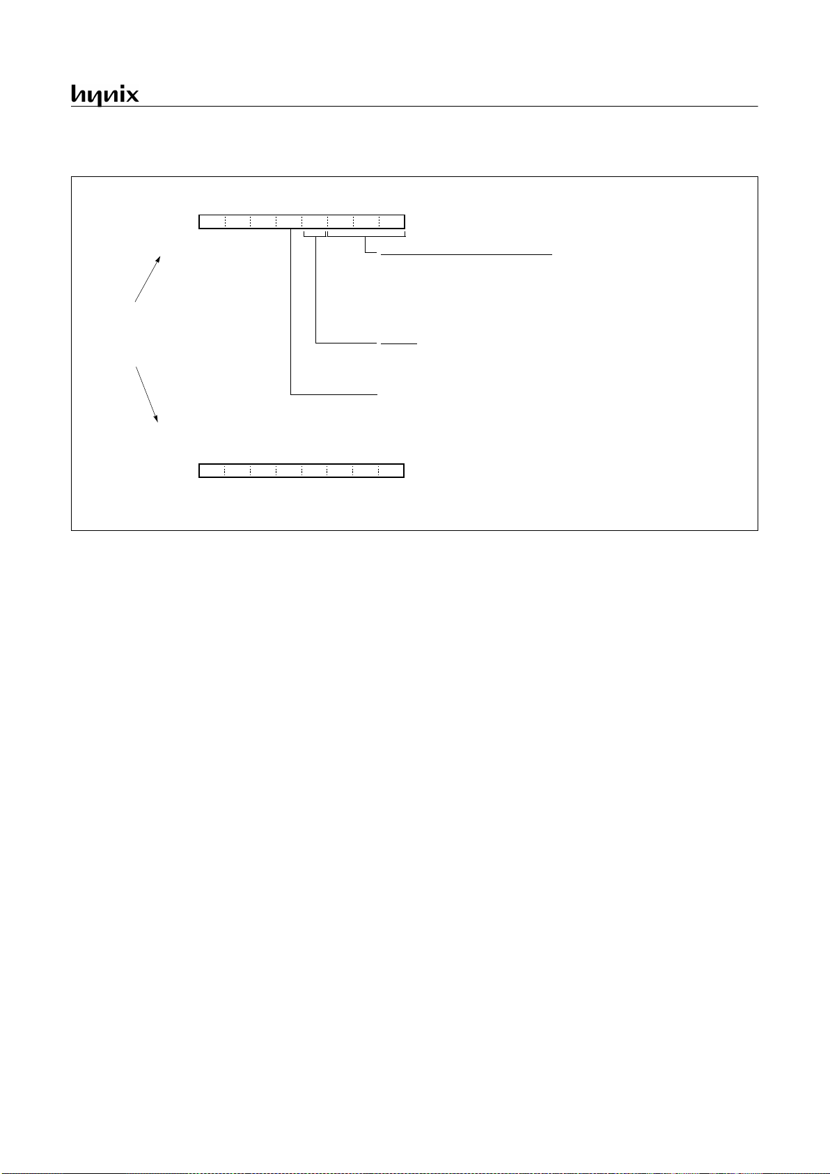
GMS81C7008/7016
APR., 2001 Ver 2.01 43
Figure 12-2 BITR: Basic Interval Timer Mode Register
Example 1
:
Interrupt request flag is generated every 8.192ms at 4MHz.
:
LDM CKCTLR,#0CH
SET1 BITE
EI
:
BTCL
76543210
--
BTS1
Basic Interval Timer source clock select
000: f
XIN
÷ 8
001: f
XIN
÷ 16
010: f
XIN
÷ 32
011: f
XIN
÷ 64
100: f
XIN
÷ 128
101: f
XIN
÷ 256
110: f
XIN
÷ 512
111: f
XIN
÷ 1024
Clear bit
0: Normal operation, free-run
1: Clear 8-bit counter (BITR) to “0” and count up again.
INITIAL VALUE: ---0 0111
B
ADDRESS: 0F4
H
CKCTLR
INITIAL VALUE: Undefined
ADDRESS: 0F4
H
BITR
Both register are in same address,
when write, to be a CKCTLR,
when read, to be a BITR.
Caution:
8-BIT FREE-RUN BINARY COUNTER
BTS0BTS2
BTCL
BTCL
76543210
or f
SXIN
÷ 8
or f
SXIN
÷ 16
or f
SXIN
÷ 32
or f
SXIN
÷ 64
or f
SXIN
÷ 128
or f
SXIN
÷ 256
or f
SXIN
÷ 512
or f
SXIN
÷ 1024
R
WW WWW
RR RRR RR
BCK
-
This bit becomes to “0” automatically after one machine cycle.
For the test purpose.
This bit must be cleared to “0” for normal operation,
otherwise BIT clock source is form sub-clock.
Page 48

GMS81C7008/7016
44 APR., 2001 Ver 2.01
13. TIMER/EVENT COUNTER
The GMS81C7008/16 has four Timer/Event count ers. Each module can generate an interrupt to indicate that an event has occurred
(i.e. timer match).
Timer 0 and Timer 1 are can be used either two 8-bit Timer/
Counter or one 16-bit Timer/Counter with combine them. Also
Timer 2 and Timer 3 can be joined as a 16-bit Timer/Counter.
In the “timer” function, the register is increased every internal
clock input. Thus, one can think of it as counting internal clock
input. The count rate is 1/2 to 1/2048 of the oscillator frequency.
In the “counter” function, the register is incremented in response
to a 0-to-1 (rising edge) transition at its corresponding external
input pin, EC0 or EC2 pin.
In addition the “capture” fun ction, th e register is inc remented i n
response external or internal clock sources same with timer or
counter function. When external clock edge input, the count register is captured into Capture data register correspondingly.
It has five operating modes: “8-bit timer/counter”, “16-bit timer/
counter”, “8-bit capt ure”, “16-bit capture”, “PWM mode” which
are selected by bit in Timer mode register TMn.
In operation of Timer 2, Timer 3, their operations are same with
Timer 0, Timer 1, respectively.
When programming the software, you may refer to following example
.
Example 1:
Timer 0 = 8-bit timer mode, 8ms interval at 4MHz
Timer 1 = 8-bit timer mode, 4ms interval at 4MHz
Timer 2 = 16-bit event counter mode
LDM SCMR,#0 ;Main clock mode
LDM TDR0,#249
LDM TM0,#0001_0011B
LDM TDR1,#124
LDM TM1,#0000_1111B
LDM TDR2,#1FH
LDM TDR3,#4CH
LDM TM2,#0001_1111B
LDM TM3,#0100_1100B
SET1 T0E
SET1 T2E
EI
:
:
Example 2:
Timer0 = 16-bit timer mode, 0.5s at 4MHz
Timer2 = 2ms 8-bit timer mode at 4MHz
Timer3 = 250us 8-bit timer mode at 4MHz
LDM SCMR,#0 ;Main clock mode
LDM TDR0,#23H
LDM TDR1,#0F4H
LDM TM0,#0FH ;FXIN/32, 8us
LDM TM1,#4CH
LDM TDR2,#249
LDM TDR3,#124
LDM TM2,#0FH ;FXUN/32, 8us
LDM TM3,#0DH ;FXIN/8, 2us
SET1 T0E
SET1 T2E
SET1 T3E
EI
:
:
Example 3:
Timer0 = 8-bit timer mode, 2ms interval at 4MHz
Timer1 = 8-bit capture mode, 2us sampling count.
LDM TDR0,#249 ;250x8=2000us
LDM TM0,#0FH ;FXIN/32, 8us
LDM IEDS,#XXXX_01XXB ;FALLING
LDM PMR,#XXXX_XX1XB ;AS INT1
LDM TDR1,#0FFH
LDM TM1,#0001_1011B ;2us
SET1 T0E ;ENABLE TIMER 0
SET1 T1E ;ENABLE TIMER 1
SET1 INT1E ;ENABLE EXT. INT1
EI
:
:
X: don’t care.
Example 4:
Timer0 = 8-bit timer mode, 2ms interval at 4MHz
Timer2 = 16-bit capture mode, 8us sampli ng count.
LDM TDR0,#249
LDM TM0,#0FH
LDM IEDS,#XX11_XXXXB
LDM PMR4,#XXXX_X1XXB
LDM TDR2,#0FFH ;MAX
LDM TDR3,#0FFH ;MAX
LDM TM2,#XX10_1111B ;/32
LDM TM3,#X10X_11XXB
SET1 T0E ;ENABLE TIMER 0
SET1 T2E ;ENABLE TIMER 2
SET1 INT2E ;ENABLE EXT. INT2
EI
:
:
X: don’t care.
Page 49

GMS81C7008/7016
APR., 2001 Ver 2.01 45
Figure 13-1 TM0, TM1, TDRn Registers
BTCL
76543210
CAP0 T0CK1
INITIAL VALUE: 00
H
ADDRESS: 0E0
H
TM0
T0CK0 T0CN T0ST
76543210
INITIAL VALUE: 0FF
H
ADDRESS: 0E1H, 0E3H, 0E7H, 0E9H
TDR0~TDR3
Compare data registers
WWWWWWWW
R/W R/W R/W R/W R/W R/W
T0CK2
Timer 0 mode register
Basic Interval Timer source clock select
000: f
XIN
÷ 2
001: f
XIN
÷ 4
010: f
XIN
÷ 8
011: f
XIN
÷ 32
100: f
XIN
÷ 128
101: f
XIN
÷ 512
110: f
XIN
÷ 2048
111: EC0 (External event input 0)
0: Disable count
1: Enable count
0: stop count
1: clearing the T0 counter and start count again
Timer/Counter 0 enable flag
Timer/Counter 0 start/stop control flag
0: Timer mode
1: Capture mode
Capture mode enable
--
BTCL
76543210
PWME0
T1CK1
INITIAL VALUE: 00
H
ADDRESS: 0E2
H
TM1
T1CK0 T1C N T1ST
R/W R/W R/W R/W R/W R/W
CAP1
Timer 1 mode register
Timer/Counter 1 source clock select
00: f
XIN
01: f
XIN
÷ 2
10: f
XIN
÷ 8
11: Timer 0 clock
0: Disable count
1: Enable count
0: stop count
1: clearing the T1 counter and start count again
Timer/Counter 1 enable flag
Timer/Counter 1 start/stop control flag
0: Timer mode
1: Capture mode
Capture mode enable
POL0 16BIT0
R/W R/W
0: Disable
1: Enable
PWM enable bit
0: Active low
1: Active high
PWM duty control
0: 8-bit mode
1: 16-bit mode
Mode selection
or f
SXIN
or f
SXIN
÷ 2
or f
SXIN
÷ 8
(depend on SCMR)
or f
SXIN
÷ 2
or f
SXIN
÷ 4
or f
SXIN
÷ 8
or f
SXIN
÷ 32
or f
SXIN
÷ 128
or f
SXIN
÷ 512
or f
SXIN
÷ 2048
Page 50

GMS81C7008/7016
46 APR., 2001 Ver 2.01
Figure 13-2 TM2, TM3 Registers
BTCL
76543210
CAP2 T2CK1
INITIAL VALUE: 00
H
ADDRESS: 0E6
H
TM2
T2CK0 T2CN
T2ST
R/W R/W R/W R/W R/W R/W
T2CK2
Timer 2 mode register
Timer/Counter 2 source clock select
000: f
XIN
÷ 2
001: f
XIN
÷ 4
010: f
XIN
÷ 8
011: f
XIN
÷ 32
100: f
XIN
÷ 128
101: f
XIN
÷ 512
110: f
XIN
÷ 2048
111: EC2 (External event input 2)
0: Disable count
1: Enable count
0: stop count
1: clearing the T0 counter and start count again
Timer/Counter 2 enable flag
Timer/Counter 2 start/stop control flag
0: Timer mode
1: Capture mode
Capture mode enable
--
BTCL
76543210
PWME1
T3CK1
INITIAL VALUE: 00
H
ADDRESS: 0E8
H
TM3
T3CK0 T3CN T3ST
R/W R/W R/W R/W R/W R/W
CAP3
Timer 3 mode register
Timer/Counter 3 source clock selection
0: Disable count
1: Enable count
0: stop count
1: clearing the T3 counter and start count again
Timer/Counter 3 enable flag
Timer/Counter 3 start/stop control flag
0: Timer mode
1: Capture mode
Capture mode enable
POL1 16BIT1
R/W R/W
0: Disable
1: Enable
PWM enable bit
0: Active low
1: Active high
PWM1 duty control
0: 8-bit mode
1: 16-bit mode
Mode selection
00: f
XIN
01: f
XIN
÷ 2
10: f
XIN
÷ 8
11: Timer 2 clock
or f
SXIN
or f
SXIN
÷ 2
or f
SXIN
÷ 8
(depend on SCMR)
or f
SXIN
÷ 2
or f
SXIN
÷ 4
or f
SXIN
÷ 8
or f
SXIN
÷ 32
or f
SXIN
÷ 128
or f
SXIN
÷ 512
or f
SXIN
÷ 2048
76543210
INITIAL VALUE: 00
H
ADDRESS: 0E1H, 0E4H, 0E7H, 0EAH
T0~T3
Count registers
RRRRRRRR
CDR0~CDR3
Page 51

GMS81C7008/7016
APR., 2001 Ver 2.01 47
13.1 8-bit Timer / Counter Mode
The GMS81C7008/16 has four 8-bit Timer/Counters, Timer 0,
Timer 1, Timer 2, Timer 3 which are shown in Figure 13-3, Figure 13-4.
The “timer” or “counter” function is selected by control registers
TMn. To use as an 8-bit timer/counter mode, CAP0, CAP1,
16BIT0 and PWME bits shou ld be cleared to “0” . These timers
have each 8-bit count register and data register. The count register
is increased by every internal or external clock input. The internal
clock has a prescaler divide ratio option of 2~2048 selected by
control bits of register TMn (n=0,1,2,3).
Figure 13-3 8-bit Timer/Counter 0, 1
EC0 PIN
÷
2
÷
4
÷
8
MUX
Prescaler
T0IF
clear
0: Stop
1: Clear and start
000
001
010
TIMER 0
INTERRUPT
MUX
T1IF
clear
0: Stop
1: Clear and start
TIMER 1
INTERRUPT
÷
8
÷
2
÷
1
TDR0 (8-bit)
T1 (8-bit)
TDR1 (8-bit)
T0 (8-bit)
Comparator
Comparator
TIMER 0
TIMER 1
R31/T1O/PWM0
F/F
BTCL
76543210
- CAP0 T0CK1
INITIAL VALUE: 00
H
ADDRESS: 0E0
H
TM0
T0CK0 T0CN T0ST-T0CK2
XX
X means don’t care
0
PIN
÷
32
÷
128
÷
512
÷
2048
011
100
101
110
111
00
01
10
11
BTCLPOL0
PWME0
T1CK1
INITIAL VALUE: 00
H
ADDRESS: 0E2
H
TM1
T1CK0 T1CN T1ST
16BIT0
CAP1
X000
Edge Detector
PMR.6
f
XIN
f
SXIN
0X
1X
SCMR[1:0]
XXXX
XX X XX
T0CN
T0CK[2:0]
1
0
T0ST
T1ST
T1CN
1
0
T1CK[1:0]
[0D9
H
.6]
[0E1H]
[0E1
H
]
[0E4
H
]
[0E3
H
]
Page 52

GMS81C7008/7016
48 APR., 2001 Ver 2.01
Note: The contents of Timer data regist er TDRx shoul d be
initialized with 1
H
~FFH, not to 0H, because it is not to de-
fined before reset.
In the Timer 0, timer register T0 increments from 00H until it
matches with TDR0 and then reset to 00
H
. The match output of
Timer 0 generates Timer 0 interrupt (latched in T0IF bit)
As TDRx and Tx register are in same address, when reading it as
a Tx, written to TDRx.
In counter function, the counter is increased every 0-to-1 (rising
edge) transition of EC0 or EC2 pin. In order to use counter function, the bit 3 and bit 4 of the Port mode register PMR are set to
“1” by software. The Timer 0 can be used as a counter by pin EC0
input. Similarly, Timer 2 can be used by pin EC2 input.
Figure 13-4 8-bit Timer/Counter 2, 3
EC2 PIN
÷
2
÷
4
÷
8
MUX
Prescaler
T2IF
clear
0: Stop
1: Clear and start
000
001
010
TIMER 2
INTERRUPT
MUX
T3IF
clear
0: Stop
1: Clear and start
TIMER 3
INTERRUPT
÷
8
÷
2
÷
1
TDR2 (8-bit)
T3 (8-bit)
TDR3 (8-bit)
T2 (8-bit)
Comparator
Comparator
TIMER 2
TIMER 3
R32/T3O/PWM0
F/F
BTCL
76543210
- CAP2 T2CK1
INITIAL VALUE: 00
H
ADDRESS: 0E6
H
TM2
T2CK0 T2CN T2ST-T2CK2
XX
X means don’t care
0
PIN
÷
32
÷
128
÷
512
÷
2048
011
100
101
110
111
00
01
10
11
BTCLPOL1
PWME1
T3CK1
INITIAL VALUE: 00
H
ADDRESS: 0E8
H
TM3
T3CK0 T3CN T3ST
16BIT1
CAP3
X000
Edge Detector
PMR.7
f
XIN
f
SXIN
0X
1X
SCMR[1:0]
XXXX
XX X XX
T2CN
T2CK[2:0]
1
0
T2ST
T3ST
T3CN
1
0
T3CK[1:0]
[0D9
H
.7]
[0E7H]
[0E7
H
]
[0EA
H
]
[0E9
H
]
Page 53

GMS81C7008/7016
APR., 2001 Ver 2.01 49
8-bit Timer Mode
In the timer mode, the internal clock is used for counting up.
Thus, you can think of it as counting internal clock input. The
contents of TDRn (n=0,1,2,3) are compared with the co nten ts of
up-counter, Tn (n=0,1,2,3). If match is found, a timer 1 interrupt
(T1IF) is generated and the up-counter is cleared to 0. Counting
up is resumed after the up-counter is cleared.
As the value of TDRn can be re-written by software, time interval
is set as you want
Figure 13-5 Timer Mode Timing Chart
Figure 13-6 Timer Count Example
0
n-2
2
0
n
3
n-1
n
Source clock
Up-counter
TDR1
T1IF interrupt
Start count
1
23
1 4
Match
Detect
Counter
Clear
~
~
~
~
~
~
~
~
~
~
~
~
Timer 1 (T1IF)
Interrupt
TDR1
TIME
Occur interrupt Occur interrupt Occur interrupt
Interrupt period
up-count
~
~
~
~
0
1
2
3
4
5
6
7A
7D
7C
Count Pulse
= 8 µs x 125
7B
MATCH
Example:
Make 1msinterrupt using by Timer0 at 4MHz
LDM TM0,#0FH ; divide by 32
LDM TDR0,#124 ; 8us x (124+1)= 1ms
SET1 T0E ; Enable Timer 0 Interrupt
EI ; Enable Master Interrupt
Period
When
TDR0 = 124
D
= 7C
H
f
XIN
= 4 MHz
INTERRUPT PERIOD =
4 × 10
6
Hz
1
×
32 × (124+1) = 1 ms
TM0 = 0000_1111
B
(8-bit Timer mode, Prescaler divide ratio → ÷32)
8 µs
(TDR0 = T0)
7D
0
Page 54
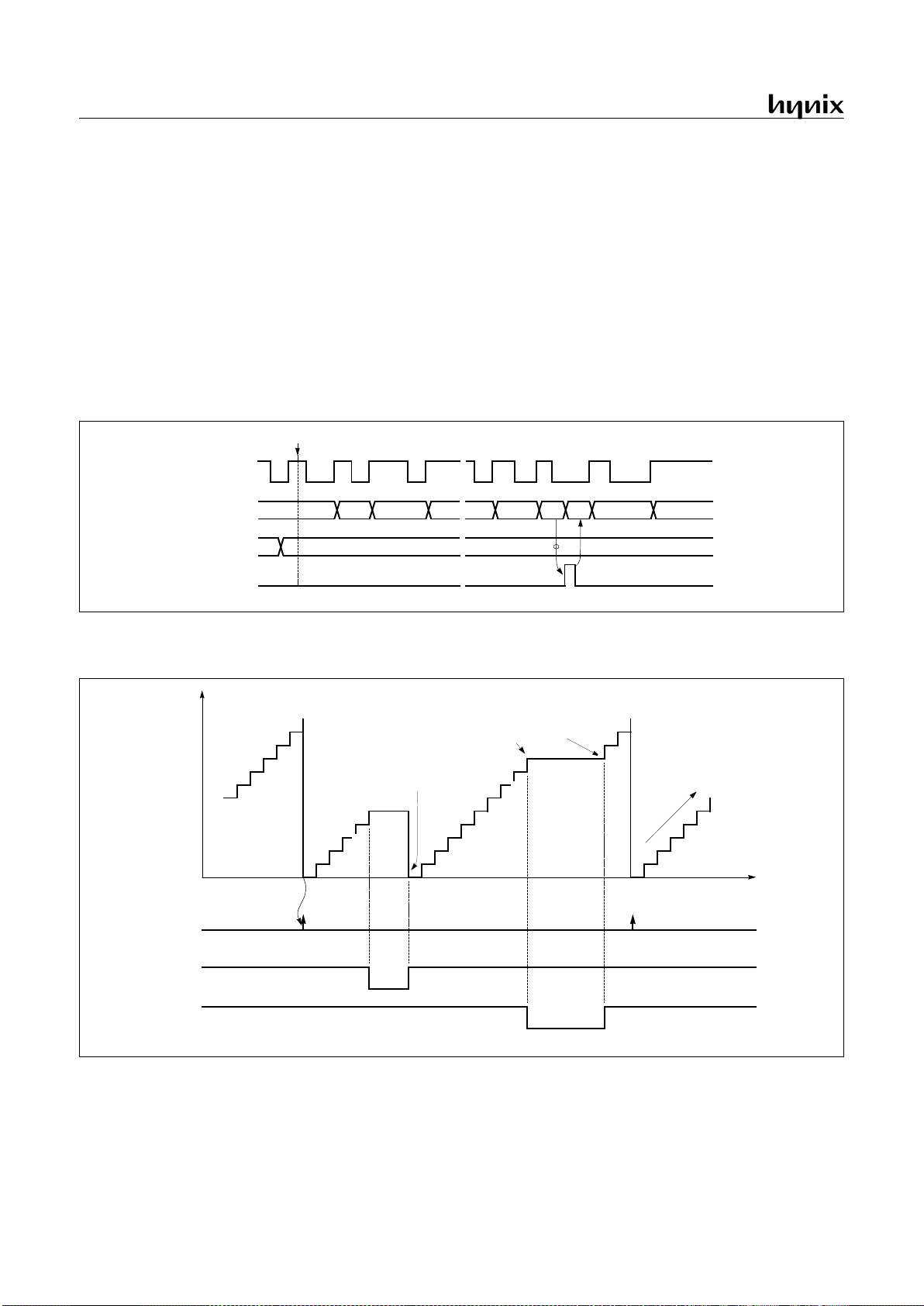
GMS81C7008/7016
50 APR., 2001 Ver 2.01
8-bit Event Counter Mode
In this mode, counting up is started by an external trigger. This
trigger means rising edge of the EC0 or EC2 pin input. Source
clock is used as an intern al cloc k sele cted with ti mer mode r eg ister TM0, TM1, TM2 or TM3. The contents of timer data registe r
TDRn (n = 0,1,2,3,........,FF) are compared with the contents of
the up-counter Tn. If a match is found, an timer interrupt request
flag TnIF is generated, and the counter is cleared to “0”. The
counter is restart and count up continuously by every rising edge
of the ECn pin input.
The maximum frequency applied to the ECn pin is f
XIN
/2 [Hz].
In order to use event counter function, the bit 3, 4 of the Port
Mode Register PMR (address 0D9H) is required to be set to “1”.
After reset, the value of timer data register TDRn is undefined, it
should be initialized to between 1
H
~FF
H
not to "0". The interval
period of Timer is calculated as below equation.
Figure 13-7 Event Counter Mode Timing Chart
Figure 13-8 Count Operation of Timer / Event counter
Period (sec)
1
f
XIN
----------
2 Divide Ratio TDRn
×××
=
0
1
2
1
0n
2
~
~
~
~
~
~
n-1
n
~
~
~
~
~
~
ECn pin input
Up-counter
TDR1
T1IF interrupt
Start count
Timer 1 (T1IF)
Interrupt
TDR1
TIME
Occur interrupt Occur interrupt
stop
clear & start
disable
enable
Start & St op
T1ST
T1CN
Control count
up-count
~
~
~
~
T1ST = 0
T1ST = 1
T1CN = 0
T1CN = 1
Page 55

GMS81C7008/7016
APR., 2001 Ver 2.01 51
13.2 16-bit Timer / Counter Mode
The Timer register is being run with all 16 bits. A 16-bit timer/
counter register T0, T1 are i ncremented from 0000
H
until it
matches TDR0, TDR1 and then resets to 0000
H
. The match out-
put generates Timer 0 interrupt.
The clock source of the Ti mer 0 is s elected eit her inte rnal or e x-
ternal clock by bit T0SL1, T0SL0.
Even if the Timer 0 (including the Timer 1) is used as a 16-bit
timer, the Timer 2 and Timer 3 can still be used as either two 8bit timer or one 16-bit timer b y settin g th e TM2 . Re v ersely , even
if the Timer 2 (including the Timer 3) is used as a 16-bit timer,
the Timer 0 and Timer 1 can still be used as 8-bit timer independently.
Figure 13-9 16-bit Timer/Counter
T0IF
clear
0: Stop
1: Clear and start
T0ST
T0CK[2:0]
TIMER 0
INTERRUPT
T0CN
Comparator
TIMER 0 + TIMER 1 → TIMER 0 (16-bit)
Higher byte Lower byte
COMPARE DATA
T0
(16-bit)
1
0
(Not Timer 1 interrupt)
76543210
INITIAL VALUE: 00
H
ADDRESS: 0E0
H
TM0
XX XXXX0X
X means don’t care
÷
2
÷
4
÷
8
MUX
Prescaler
000
001
010
÷
32
÷
128
÷
512
÷
2048
011
100
101
110
111
Edge Detector
EC0 PIN
TM1
BTCL
X10011XX
POL0
PWME0
T1CK1
INITIAL VALUE: 00
H
ADDRESS: 0E2
H
T1CK0 T1CN T1ST
16BIT0
CAP1
BTCL
- CAP0 T0CK1 T0CK0 T0CN T0ST-T0CK2
76543210
INITIAL VALUE: 00
H
ADDRESS: 0E6
H
TM2
XX XXXX0X
TM3
BTCL
X10011XX
POL1
PWME1
T3CK1
INITIAL VALUE: 00
H
ADDRESS: 0E8
H
T3CK0 T3CN T3ST
16BIT1
CAP3
BTCL
- CAP2 T2CK1 T2CK0 T2CN T2ST-T2CK2
R31/T1O/PWM0
F/F
PIN
PMR.6
T1
TDR0
TDR1
f
XIN
f
SXIN
0X
1X
SCMR[1:0]
T2IF
clear
0: Stop
1: Clear and start
T2ST
T2CK[2:0]
TIMER 2
INTERRUPT
T2CN
Comparator
TIMER 0 + TIMER 1 → TIMER 0 (16-bit)
Higher byte Lower byte
COMPARE DATA
T2
(16-bit)
1
0
(Not Timer 3 interrupt)
÷
2
÷
4
÷
8
MUX
Prescaler
000
001
010
÷
32
÷
128
÷
512
÷
2048
011
100
101
110
111
Edge Detector
EC2 PIN
R32/T3O/PWM1
F/F
PIN
PMR.7
T3
TDR2
TDR3
f
XIN
f
SXIN
1X
1X
SCMR[1:0]
[0D9H.6]
[0D9
H
.7]
X means don’t care
Page 56

GMS81C7008/7016
52 APR., 2001 Ver 2.01
13.3 8-bit Capture Mode
The capture mode can be used to measure the pulse width between two edges. The Timer 0 capture mode is set by bit CAP0
of Timer Mode Regi ster TM0, an d the Tim er 1 captu re mode is
set by CAP1 of Timer Mo de Register TM1 as sh own in Figure
13-10. Timer 2 and Timer 3 have same arch itecture with Time r 0
and Timer 1.
The Timer/Counter register is incremen ted in response internal or
external input. This counting function is same with normal timer
mode, and Timer interru pt is generate when timer r egister T0 (T1 ,
T2, T3) increase and match TDR0 (TDR1, TDR2, TDR3).
Timer/Counter still does the above, but with the added feature
that a edge transition at external input INTn pin causes the current
.
Figure 13-10 8-bit Capture Mode (Timer0/Timer1 case)
f
timer
f
xin
2 prescaler value TDR 1
+
()××
--------------------------------------------------------------------------------
=
T0CK[2:0]
÷
2
÷
4
÷
8
MUX
000
001
010
÷
32
÷
128
÷
512
÷
2048
011
100
101
110
111
Edge Detector
EC0 PIN
T0CN
INT0IF
0: Stop
1: Clear and start
INT0
INTERRUPT
CDR0 (8-bit)
T0 (8-bit)
01
10
11
capture
IEDS[1:0]
CDR0 (8-bit)
CDR0
T0IF
TIMER 0
INTERRUPT
Comparator
COMPARE DATA
CDR0 (8-bit)
TDR0 (8-bit)
INT0 PIN
T0ST
clear
clear
T1CK[1:0]
÷
1
÷
2
÷
8
MUX
00
01
10
11
T1CN
0: Stop
1: Clear and start
CDR0 (8-bit)
T1 (8-bit)
CDR0 (8-bit)
CDR1
T1IF
TIMER 1
INTERRUPT
Comparator
COMPAR E DATA
CDR0 (8-bit)
TDR1 (8-bit)
T1ST
clear
INT1IF
INT1
INTERRUPT
01
10
11
capture
IEDS[3:2]
INT1 PIN
clear
76543210
INITIAL VALUE: 00
H
ADDRESS: 0E0
H
TM0
XX XXXX1X
TM1
BTCL
X001XXXX
POL0
PWME0
T1CK1
INITIAL VALUE: 00
H
ADDRESS: 0E2
H
T1CK0 T1CN T1ST
16BIT0
CAP1
BTCL
- CAP0 T0CK1 T0CK0 T0CN T0ST-T0CK2
÷
1
Prescaler
f
XIN
f
SXIN
0X
1X
SCMR[1:0]
R31/T1O/PWM0
F/F
PIN
PMR.6
[0D9
H
.6]
f
EX
Page 57

GMS81C7008/7016
APR., 2001 Ver 2.01 53
value in the Timer counter register (T0,T1), to be captured and
stored into registers CDRn (CDR0, CDR1), respectively. Aft er
capture, the Timer counter register is cleared and restarts by hardware. At this time, reading the address E1
H
as a CDR0, not T0.
T0, TDR0, CDR0 are located at same address. The other
CDR1~CDR3 are same. Refer to Timer registers of page 27.
It has three transition modes: “falling edge”, “rising edge”, “both
edge” which are selected by interrupt edge selection register
IEDS. Refer to “17.4 External Interrupt” on page 68. In additi on,
the transition at INTn pin generate an interrupt.
Note: The CDRn and Tn are in same address.In the capture mode, reading operation is read as CDRn, not Tn because addressing path is opened to the CDRn.
Figure 13-11 16-bit Capture Mode
13.4 16-bit Capture Mode
16-bit capture mode is the s ame as 8-bi t capture, except that the
Timer register is bein g run will 16 b its. Configu ration is sh own in
Figure 13-11.
13.5 Timer output port mode
The GMS81C7008/16 has a function of Timer compare output.
To pulse out, the timer ma tch can goes out to port pin (T1O, T3O)
as shown in Figure 13-3, Figure 13-4 and Figur e 13-9.
Thus pulse out is generated by the timer match. These operation
is implemented to pin T1O, T3O. This pin output the signal having 50% duty square wave and output frequency is same as below
equation.
To use this function, the bit 6 and bit 7 of Port Mode Register
(PMR) are set or clear properly. In addition, 16-bit Timer output
mode is available, also
T0CK[2:0]
÷
2
÷
4
÷
8
MUX
000
001
010
÷
32
÷
128
÷
512
÷
2048
011
100
101
110
111
Edge Detector
EC0 PIN
T0CN
INT0IF
0: Stop
1: Clear and start
INT0
INTERRUPT
01
10
11
capture
IEDS[1:0]
T0IF
TIMER 0
INTERRUPT
Comparator
COMPARE DATA
INT0 PIN
T0ST
clear
clear
Prescaler
f
XIN
f
SXIN
0X
1X
SCMR[1:0]
R31/T1O/PWM0
F/F
PIN
PMR.6
CDR1 CDR0
TDR1 TDR0
T1 T0
BTCL
76543210
- CAP0 T0CK1
INITIAL VALUE: 00
H
ADDRESS: 0E0
H
TM0
T0CK0 T0CN T0ST-T0CK2
XX
X means don’t care
1
BTCLPOL0
PWME0
T1CK1
INITIAL VALUE: 00
H
ADDRESS: 0E2
H
TM1
T1CK0 T1CN T1ST
16BIT0
CAP1
X
101
11XX
XX X XX
[0D9H.6]
16 BITSMSB LSB
f
EX
Page 58

GMS81C7008/7016
54 APR., 2001 Ver 2.01
13.6 PWM Mode
The GMS81C70xx and GMS81C71xx have two high speed
PWM (Pulse Width Modulation) fu nctions which shared with
Timer 1 and Timer 3.
Figure 13-12 PWM Mode
T1CK[1:0]
MUX
÷
8
÷
2
÷
1
11
10
01
00
T1CN
T1PPR (8-bit)
S
Comparator
clear
T1ST
76543210
TM1
BTCL
X010XXXX
POL0
PWME0
T1CK1
INITIAL VALUE: 00
H
ADDRESS: 0E2
H
T1CK0 T1CN T1ST
16BIT0
CAP1
Prescaler
f
XIN
f
SXIN
0X
1X
SCMR[1:0]
2 Bit
T1 (8-bit)
(note1)
T1PDR (8-bit)
2 Bit
R
Q
T1PDR (8-bit)
2 Bit
T0 clock source
(from Timer 0)
POL0
R31/T1O/PWM0
PIN
PMR.6
PWM0HR
----XXXX
-
PWM02
INITIAL VALUE: 00
H
ADDRESS: 0E5
H
PWM03
-
PWM00PWM01
--
Duty highPeriod high
PWM[01:00]
[0E4
H
][0E5H]
PWM[03:02]
[0E3H][0E5H]
[0D9
H
.6]
2 Bit
Note1
: In the PWM mode, 2 bits are added
by hardware automatically.
T3CK[1:0]
MUX
÷
8
÷
2
÷
1
11
10
01
00
T3CN
T3PPR (8-bit)
S
Comparator
clear
T3ST
76543210
TM3
BTCL
X010XXXX
POL1
PWME1
T3CK1
INITIAL VALUE: 00
H
ADDRESS: 0E8
H
T3CK0 T3CN T3ST
16BIT1
CAP3
Prescaler
f
XIN
f
SXIN
0X
1X
SCMR[1:0]
2 Bit
T3 (8-bit)
(note1)
T3PDR (8-bit)
2 Bit
R
Q
T3PDR (8-bit)
2 Bit
T2 clock source
(from Timer 2)
POL1
R32/T3O/PWM1
PIN
PMR.7
PWM1HR
----XXXX
-
PWM12
INITIAL VALUE: 00
H
ADDRESS: 0EB
H
PWM13
-
PWM10PWM11
--
Duty highPeriod high
PWM[11:10]
[0EA
H
][0EBH]
PWM[13:12]
[0E9H][0EBH]
[0D9
H
.7]
2 Bit
f
EX
Page 59

GMS81C7008/7016
APR., 2001 Ver 2.01 55
Note: Whenever change the register content of Period or
Duty of PWM output, the ti mer co unter Tn must be sto pped
and restart again by software.
The PWM0 will be explained in this chapter. Other PWM1 has
same architecture. Pin R32/T1O/PWM0 outputs up to a 10-bit
resolution PWM output. This pin should be configure as a PWM
output to set bit PRM0.6 to “1”.
The period of the PWM output is determined by the T1PPR
(PWM0 Period Register) and PWM0HR[3:2] and the duty is determined by the T1PDR (PWM0 Duty Register) and
PWM0HR[1:0].
The user writes the lower 8-bit p eriod valu e to the T1P PR and the
higher 2-bit period value to the PWM0HR[3:2].
And writes duty value to the T1PDR and the PWM0HR[1:0]
same way.
The T1PDR is configure as a double buffering for glitchless
PWM output. In, the duty data is transferred from the master to
the slave when the period data matched to th e counted valu e. (i.e.
at the beginning of next duty cycle)
The relation be twe en freq uency an d resol ution i s in in verse pr oportion. Table 13-1 shows the PWM frequency in each clock
source. If it needed higher frequency of PWM, it should be reduced resoluti on.
Figure 13-13 Example of Register setting
The bit POL0 of TM0 decides the polar ity of duty cycle .
If the duty value is set same to the period value, the PWM output
is determined by the bit POL0 (1: High, 0 : Lo w) . And if the d uty
value is set to “00
H
”, the PWM output is determined by the bit
POL0 (1: Low, 0: High).
It can be ch anged du ty value w hen the P WM output. However the
changed duty v alue is outp ut afte r th e cur rent p eri od is ov er . And
it can be maintained the duty value at present output when
changed only period value shown as Figure 13-14. As it were, the
absolute duty time is not changed in varying frequency. But the
changed period val ue must greater than the duty value.
At PWM output st art c ommand, one fi rst p ulse w ould be outpu t
abnormally. Because if user writes reg ister v alue s while timer i s
in operation, these register could be set with certain values at first.
To prevent this operation, user must stop PWM timer clock and
then set the duty and the period register values.
T1
~
~
~
~
01
H
02
H
03
H
04
H
256H257H258
H
3E7
H
01
H
~
~
~
~
~
~
PWM output
Duty; (257H+1) x 500nS = 300uS
00
H
00
H
~
~
~
~
02
H
Clock source
Period; (3E7H+1) x 500nS = 500uS
T1PPR
PWM0HR
11 11100111
T1PDR
10 01010111
[0E4
H
]
[0E3
H
]
[0E5
H
]
----1110
Period
Duty
~
~
Page 60

GMS81C7008/7016
56 APR., 2001 Ver 2.01
Example:
Timer1 = 2kHz, 30% duty PWM mode
LDM TM1,#00H
LDM T1PPR,#0E8H
LDM T1PDR,#58H
LDM PWM0HR,0000_1110B
LDM TM1,#1010_1011B
Refer to Figure 13-13.
Figure 13-14 Example of changing the period in absolute duty cycle at 4MHz
Resolutio
n
PWM clock source
f
XIN
÷÷÷÷
1f
XIN
÷÷÷÷
2f
XIN
÷÷÷÷
1024
10-bit 3.9kHz 1.95kHz 3.8Hz
9-bit 7.8kHz 3.9kHz 7.6Hz
8-bit 15.6kHz 7.8kHz 15.3Hz
7-bit 31.2kHz 15.6kHz 30.5Hz
Table 13-1 PWM Frequency vs. Resolution at 4MHz
Source
T1
PWM
POL=1
Duty Cycle
Period Cycle [ (D
H
+1) x 2uS = 28uS, 35.7kHz ]
PWMHR = 00
H
T1PPR = 0D
H
T1PDR = 04
H
T1CK[1:0] = 10 (2uS)
00
01 02 03
04
05 07 08 0A 0B 0C
0D
00
01 02 03
04
05
06
07 08
09
00
01 02 0306 09
04
[ (4+1) x 2uS = 10uS ]
Duty Cycle
[ (4+1) x 2uS =10uS ]
Period Cycle [ (9+1) x 2uS = 20uS, 50kHz ]
Duty Cycle
[ (4+1) x 2uS = 10uS ]
Write “09H” to T1PPR
Period changed
clock
Page 61

GMS81C7008/7016
APR., 2001 Ver 2.01 57
14. ANALOG DIGITAL CONVERTER
The analog-to-digital converter (A/D) allows conversion of an
analog input signal to a co rrespon d ing 8-bit d ig ita l v alue. Th e A/
D module has eight analog inputs, which are multiplexed int o one
sample and hold. The output of the sample and hold is the input
into the converter, which generates the re sult via success ive approximation. The analog supply voltage is connected to AV
DD
of
ladder resistance of A/D module.
The A/D module has two registers which are the control register
ADCM and A/D result register ADR. The register ADCM, shown
in Figure 14-4, contro ls the op er a tion of the A/D converter mod ule. The port pins can be configured as analog inputs or digital I/
O. To use analog inputs, I/O is selected input mode by R2DD direction register.
How to Use A/D Converter
The processing of conversion is start when the start bit ADST is
set to “1”. After one cycle, it is cleared by hardware. The register
ADR contains the results of the A/D co nversion . When the c onversion is completed, the result is loaded into the ADR, the A/D
conversion status bit ADSF is set to “1”, and the A/D interrupt
flag AIF is set. The block diagram of the A/D module is shown in
Figure 14-1. The A/D status bit ADSF is set automatically when
A/D conversion is completed, cleared when A/D conversion is in
process. The conversion time takes maximum 20 uS (at f
XIN
=4
MHz).
Figure 14-1 A/D Block Diagram
A/D Converter Cautions
(1) Input voltage range of AN0 to AN7
The input voltage of AN0 to AN7 should be withi n the specifica-
tion range. In particular, if a voltage above AVDD or below AV
SS
is input (even if within the absolute maximum rating range), the
conversion value for that channel can not be indeterminate. The
conversion values of the other channels may also be affected.
(2) Noise countermeasures
In order to maintain 8-bit resolution, attention must be paid to
noise on pins AV
DD
and AN0 to AN7. Since the effect increases
in proportion to the outp ut imped anc e of the analo g input source,
it is recommended that a capacitor be connected externally as
shown in Figure 14- 2 in order to reduce noise.
.
Figure 14-2 Analog Input Pin Connecting Capacitor
R20/AN0
R21/AN1
R22/AN2
R23/AN3
R24/AN4
R25/AN5
R26/AN6
R27/AN7
S/H
Sample & Hold
“0”
“1”
ADEN
AV
DD
8-bit DAC
LADDER RESISTOR
ADIF
A/D
INTERRUPT
SUCCESSIVE
APPROXIMATION
CIRCUIT
ADR
A/D result register
ADDRESS: ED
H
RESET VALUE: Undefined
000
001
010
011
100
101
110
111
ADS[2:0]
AN0~AN7
100~1000pF
Analog
Input
Page 62

GMS81C7008/7016
58 APR., 2001 Ver 2.01
(3) AD pin sharing with normal I/O port
The analog input pins AN0 to AN7 also function as input/output
port (PORT R20~R27) pins. When A/D conversion is performed
with any of pins AN0 to AN7 selected, be sure not to ex ecute a
PORT input instruction while conversion is in progress, as this
may reduce the conversion resolution.
Also, if digital pulses are ap plied to a pi n adjacent to the pin in the
process of A/D conversion, the expected A/D conversion value
may not be obtainable due to coupling noise. Therefore, avoid applying pulses to pins adjacent to the pin undergoing A/D conversion.
(4) AV
DD
pin input impedance
A series resistor string of approximately 10kΩ is connected between the AV
DD
pin and the AV
SS
pin.
Therefore, if th e output impedance of the reference voltag e
source is high, this will result in parallel connection to the series
resistor string between the AV
DD
pin and the AV
SS
pin, and there
will be a large reference voltage error.
Figure 14-3 A/D converter Operation Flow
Figure 14-4 A/D Converter Control Register
ENABLE A/D CONVERTER
A/D START ( ADST = 1 )
NOP
ADSF = 1
A/D INPUT CHANNEL SELECT
ANALOG REFERENCE SELECT
READ ADR
YES
NO
BTCL
76543210
ADEN
-
ADST
A/D status bit
Analog input channel select
INITIAL VALUE: -0-0 0001
B
ADDRESS: 0EC
H
ADCM
ADSF
A/D converter Enable bit
0: A/D converter module turn off and
current is not flow.
1: Enable A/D converter
R/W R/W R/W R/W R/W R
000: Channel 0 (AN0)
001: Channel 1 (AN1)
010: Channel 2 (AN2)
011: Channel 3 (AN3)
100: Channel 4 (AN4)
101: Channel 5 (AN5)
110: Channel 6 (AN6)
111: Channel 7 (AN7)
0: A/D conversion is in progress
1: A/D conversion is completed
A/D start bit
Setting this bit starts an A/D conversion.
After one cycle, bit is cleared to “0” by hardware.
ADS1 ADS0-ADS2
INITIAL VALUE: Undefined
ADDRESS: 0ED
H
ADR
A/D Conversion Data
BTCL
76543210
RRRR RR
R
R
0: 1: A/D start
--
Page 63

GMS81C7008/7016
APR., 2001 Ver 2.01 59
15. SERIAL COMMUNICATION
The serial interface is used to transmit/receive 8-b it dat a serially .
Serial commun ication bl ock consists of serial I/O da ta register,
serial I/O mode register, clock selection circuit, octal counter and
control circuit as illustrated in Fi gure 15-1.Pin R07/SIN, R06/
SOUT and R05/SCLK p ins are controll ed by the Seria l Mode
Register. The contents of the Serial I/O data register can be written into or read out by software.
The serial communication is activated by the instruction “SET1
SIOST”. The octal counter is reset to “0” by this instruc tion, starts
counting at the falling or rising edge (by POL selection) of the
transmit clock (SCLK), and it increments at the every clock. A serial interrupt request flag is se t when the eighth transmit clock
signal is input (the serial interface is reset) or when serial communication is discontinued (the octal counter is reset).
The data in the Serial Data Register can be shif ted synchron ously
with the transfer clock signal .
Figure 15-1 SCI Control Register
SCK1 SCK0 SCLK/R05 Port Clock Source Prescaler Divide Ratio
0 0 SCLK output Internal clock
÷
4
0 1 SCLK output Internal clock
÷
16
1 0 SCLK output Internal clock Use clock from Timer 0 overflow
1 1 SCLK input External clock -
BTCL
76543210
MSB
POL
SIOST
Serial transmission status bit
Serial transmission Clock selection
INITIAL VALUE: 0000_0001
B
ADDRESS: 0FE
H
SIOM
SIOSF
MSB first or LSB first
0: LSB First
1: MSB First
R/W R/W R/W R/W R/W R
00: f
XIN
÷
4
01: f
XIN
÷
16
10: Timer 0 Overflow
11: External Clock
0: Serial transmission is in progr ess
1: Serial transmission is completed
Serial transmission start bit
Setting this bit starts an Serial transmission.
After one cycle, bit is cleared to “0” by hardware.
SCK1 SCK0SIO1 SIO0
R/W
Serial transmission Operation Mode
00: Normal Port(R05,R06,R07)
01: Sending Mode(SCLK,S OUT,R07)
10: Receiving Mode(SCLK,R06,SIN)
11: Sending & Receiving Mode(SCLK,SOUT,SIN)
INITIAL VALUE: Undefined
ADDRESS: 0FF
H
SIOR
BTCL
76543210
R/W R/W R/W R/W R/W R/W
R/W
R/W
Sending Data during Sending Mod e
Receiving Data during Receiving Mode
Selection Polarity
0: Data in on rising edge, data out on falling edge
1: Data in on falling edge, data out on rising edge
R/W
Page 64

GMS81C7008/7016
60 APR., 2001 Ver 2.01
Serial I/O Mode Register(SIOM) controls serial I/O function.
The POL bit control which edge
According to SCK1 and SCK0, the internal clock or external
clock can be selected.
Serial I/O Data Register(SIOR) is an 8-bit shift register.
Figure 15-2 Block Diagram of SCI
15.1 Transmission/Receiving Timing
The serial transmission is started by setting SIOST(bit1 of
SIOM) to “1”. After one cycle of SCK, SIOST is cleared
automatically to “0”. The serial output data from 8-bit shift
register is output at falling edge of SCLK. And input data
is latched at rising edge of SCLK pin. When transmis sion
clock is counted 8 times, serial I/O counter is cleared as
‘0”. Transmission clock is halted in “H” state and serial I/
O interrupt(SIOIF) occurred.
Figure 15-3 SPI Timing Diagram at POL=0
R05/SCLK PIN
CONTROL CIRCUIT
R06/SOU T PIN
Serial IO Data
Octal Counter
Serial communicatio n
Interrupt
SIOIF
R07/SIN PIN
SCK, SIO
overflow
SCK[1:0]
MUX
÷
16
÷
4
11
10
01
00
Prescaler
f
XIN
f
SXIN
0X
1X
SCMR[1:0]
T0OV
(Timer 0 overflow)
POL
SIOST
start
SIOSF
complete
clock
clear
SIO1
SIO0
[0FF
H
]
Edge Detector
SIO[1:0]
shift clock
SCLK OUT
D1 D2 D3 D4 D6 D7D0 D5
D1 D2 D3 D4 D6 D7D0 D5
SIOST
SCLK [R05]
(POL=0)
SOUT [R06]
SIN [R07]
SIOIF
(Interrupt Req.)
SIOSF
Page 65

GMS81C7008/7016
APR., 2001 Ver 2.01 61
15.2 The method of Serial I/O
1. Select transmissio n/receiving mode
When external clock is used, the frequency should be less than
1MHz and recommended duty is 50%.
2. In case of sending mode, write data to be send to SIOR.
3. Set SIOST to “1” to start serial transmission.
If both transmission mode is sel ected and transmission is per-
formed simultaneously it would be made error.
4. The SIO interrupt is generated at the completion of SIO and
SIOSF is set to “1”. I n SIO interrupt service routine, co rrect transmission should be tested.
5. In case of receiving mode, the recei ved data is acquired by
reading the SIOR.
Figure 15-4 SPI Timing Diagram at POL=1
15.3 The Method to Test Correct Transmission
Figure 15-5 Serial Method to Test Transmission
D1 D2 D3 D4 D6 D7D0 D5
D1 D2 D3 D4 D6 D7D0 D5
SIOST
SCLK [R05]
(POL=1)
SOUT [R06]
SIN [R07]
SCIIF
SIOSF
Serial I/O Interrupt
Service Routine
SE = 0
Write SIOM
Normal Operation
Overrun Error
Abnormal
SIOSF
0
1
- SE : Interrupt Enable Register Low IENL(Bit3)
- SR : Interrupt Request Flag Register Low IRQL(Bit3)
SR
0
1
Page 66

GMS81C7008/7016
62 APR., 2001 Ver 2.01
16. BUZZER FUNCTION
The buzzer driver bloc k consis ts of 6-bit binary co unter, buz zer
register, and clock source selector. It generates square-wave
which has very wide range frequency (500Hz ~ 250kHz at f
XIN
=
4MHz) by user software.
A 50% duty pulse can be output to R30/BUZ pin to use for piezo-
electric buzzer drive. Pin R30 is assigned for output port of Buzzer driver by setting the bit 5 of PMR (address D9
H
) to “1”. At this
time, the pin R30 must be defined as output mode (the bit 0 of
R3DD=1).
Example: 2.4kHz output at 4MHz.
LDM R3DD,#XXXX_XXX1B
LDM BUR,#0111_0011B
SET1 PMR.5 ;BUZ ON
CLR1 PMR.5 ;BUZ OFF
X means don’t care
The bit 0 to 5 of BUR determines output frequency for buzzer
driving.
Equation of frequency calculation is shown below.
f
BUZ
: Buzzer frequency
f
XIN
: Oscillator frequency
Divide Ratio: Prescaler divide ratio by BUCK[1:0]
BUR: Lower 6-bit value of BUR. Buzzer period value.
The frequency of output signal is controlled by the buzzer control
register BUR.The BUR[5:0] dete rmine output frequency for
buzzer driving.
Figure 16-1 Block Diagram of Buzzer Driver
Figure 16-2 PMR and Buzzer Register
f
BUZ
f
XIN
2 DivideRatio BUR 5:0
[]
1
+
()××
--------------------------------------------------------------------------------------- -
=
Prescaler
÷
8
÷
32
÷
16
÷
64
R30/BUZ PIN
PMR.5
R30 port data
0
1
F/F
÷
2
Comparator
6-bit Compare Data
6-bit Binary Counter
MUX
00
01
10
11
BUR[5:0] [0FDH]
BUR[7:6]
f
XIN
f
SXIN
0X
1X
SCMR[1:0]
BUR[5:0]
BUR
ADDRESS: 0FD
H
RESET VALUE: Undefined
WWWWW W
Source clock select
00: ÷ 8
01: ÷ 16
10: ÷ 32
11: ÷ 64
Define Frequency of Buzzer signal
WW
BUCK1
BUCK0
R30/BUZ Selection
PMR
ADDRESS: 0D9
H
RESET VALUE: 00
H
R/W R/W R/W R/W R/W R/W
0: R30 port (Turn off buzzer)
R/W R/W
PWM1
BUZ
PWM0
INT0INT1INT2EC0EC2
1: BUZ port (Turn on buzzer)
Page 67

GMS81C7008/7016
APR., 2001 Ver 2.01 63
Note that BUR is a write-only register.
The 6-bit counter is cleared an d starts the counting by writing sig-
nal at BUR register. It is incremental from 00H until it matches 6-
bit BUR value.
When main-frequency is 4MHz, buzzer frequency is shown as
below table. The unit is kHz.
BUR
[5:0]
BUCK[1:0]
BUR
[5:0]
BUCK[1:0]
00 01 10 11 00 01 10 11
00
01
02
03
04
05
06
07
250.000
125.000
83.333
62.500
50.000
41.667
35.714
31.250
125.000
62.500
41.667
31.250
25.000
20.833
17.857
15.625
62.500
31.250
20.833
15.625
12.500
10.417
8.929
7.813
31.250
15.625
10.417
7.813
6.250
5.208
4.464
3.906
20
21
22
23
24
25
26
27
7.576
7.353
7.143
6.944
6.757
6.579
6.410
6.250
3.788
3.676
3.571
3.472
3.378
3.289
3.205
3.125
1.894
1.838
1.786
1.736
1.689
1.645
1.603
1.563
0.947
0.919
0.893
0.868
0.845
0.822
0.801
0.781
08
09
0A
0B
0C
0D
0E
0F
27.778
25.000
22.727
20.833
19.231
17.857
16.667
15.625
13.889
12.500
11.364
10.417
9.615
8.929
8.333
7.813
6.944
6.250
5.682
5.208
4.808
4.464
4.167
3.906
3.472
3.125
2.841
2.604
2.404
2.232
2.083
1.953
28
29
2A
2B
2C
2D
2E
2F
6.098
5.952
5.814
5.682
5.556
5.435
5.319
5.208
3.049
2.976
2.907
2.841
2.778
2.717
2.660
2.604
1.524
1.488
1.453
1.420
1.389
1.359
1.330
1.302
0.762
0.744
0.727
0.710
0.694
0.679
0.665
0.651
10
11
12
13
14
15
16
17
14.706
13.889
13.158
12.500
11.905
11.364
10.870
10.417
7.353
6.944
6.579
6.250
5.952
5.682
5.435
5.208
3.676
3.472
3.289
3.125
2.976
2.841
2.717
2.604
1.838
1.736
1.645
1.563
1.488
1.420
1.359
1.302
30
31
32
33
34
35
36
37
5.102
5.000
4.902
4.808
4.717
4.630
4.545
4.464
2.551
2.500
2.451
2.404
2.358
2.315
2.273
2.232
1.276
1.250
1.225
1.202
1.179
1.157
1.136
1.116
0.638
0.625
0.613
0.601
0.590
0.579
0.568
0.558
18
19
1A
1B
1C
1D
1E
1F
10.000
9.615
9.259
8.929
8.621
8.333
8.065
7.813
5.000
4.808
4.630
4.464
4.310
4.167
4.032
3.906
2.500
2.404
2.315
2.232
2.155
2.083
2.016
1.953
1.250
1.202
1.157
1.116
1.078
1.042
1.008
0.977
38
39
3A
3B
3C
3D
3E
3F
4.386
4.310
4.237
4.167
4.098
4.032
3.968
3.906
2.193
2.155
2.119
2.083
2.049
2.016
1.984
1.953
1.096
1.078
1.059
1.042
1.025
1.008
0.992
0.977
0.548
0.539
0.530
0.521
0.512
0.504
0.496
0.488
Table 16-1 Buzzer Frequency at 4MHz
Page 68

GMS81C7008/7016
64 APR., 2001 Ver 2.01
17. INTERRUPTS
The GMS81C7008/16 interrupt circuits consist of Interrupt enable register (IENH, IENL), In terrupt request flags of IRQH,
IRQL, Priority circuit, and Master enable flag (“I” flag of PSW).
Thirteen interrupt sources are provided. The configuration of interrupt circuit is shown in Figure 17-2.
The keyscan interrupt is generated when 1-to-0 transition is detected at KS0 or KS0 pin.
The Basic Interval Timer Interrupt is generated by BITIF which
is set by an overflow in the timer register.
The Watchdog timer Interrupt is generated by WDTIF which set
by a match in Watchdog timer register.
The External Interrupts INT0 ~ INT2 each can be transition-activated (1-to-0 or 0-to-1 transit ion) by selection IEDS.
The flags that actually generate these interrupts are bit INT0IF,
INT1IF and INT2IF in register IRQH and IRQL. When an external interrupt is generated, the flag that generated it is cleared by
the hardware when the service routine is vectored to only if the
interrupt was transition-activated.
The Timer 0 ~ Timer 3 Interrupts are generated by T0IF~T3IF
which are set by a match in their respectiv e timer/counter register.
The Serial Communication Interrupts are generated by SIOIF
which is set by 8-bit serial data transmitting or receiving th rou gh
SCK, SIN, SOUT pin.
The AD converter Interrupt is g enerated b y ADIF which is set by
finishing the analog to digital conve rsion.
The Watch Timer Interrupt is generated by WTIF which is set by
an 14-bit binary counter overflow.
The interrupts are controlled by the interrupt master enable flag
I-flag (bit 2 of PSW on page 19), the interrupt enable register
(IENH, IENL), and the interrupt request flags (in IRQH and
IRQL) except Power-on reset and software BRK interrupt. Below
table shows the Interrupt priority.
Vector addresses are shown in Figure 8-6 on page 21. Interrupt
enable registers are shown in Figu re 17-3. These registers are
composed of interrupt enable flags of each interrupt source and
these flags determines whether an interrupt will be accepted or
not. When enable flag is “0”, a corresponding interrupt source is
prohibited. Note that PSW contains also a master enable bit, Iflag, which disables all interrupts at once.
Figure 17-1 Interrupt Request Flag
Reset/Interrupt Symbol Priority
Hardware Reset
Key scan Interrupt
Basic Interval Timer
Watchdog Timer
External Interrupt 0
External Interrupt 1
Timer/Counter 0
Timer/Counter 1
External Interrupt 2
Serial Communication
ADC Interrupt
Watch Timer Interrupt
Timer/Counter 2
Timer/Counter 3
RESET
KS
BIT
WDT
INT0
INT1
Timer 0
Timer 1
INT2
SCI
ADC
WT
Timer 2
Timer 3
1
2
3
4
5
6
7
8
9
10
11
12
13
WDTIF
R/W
-
Timer/Counter 3
INITIAL VALUE: -000 0000
B
ADDRESS: 0DD
H
IRQH
KSIF
MSB LSB
T0IF T1IF
INT0IF INT1IFBITIF
R/W R/W
Timer/Counter 2
Timer/Counter 1 interrupt request flag
External interrupt 1
Serial Communication
INITIAL VALUE: 0--0 0000
B
ADDRESS: 0DC
H
IRQL
MSB LSB
Timer/Counter 0
R/W R/W-R/W R/W
Basic Interval Timer
Watchdog timer
A/D Converter
External interrupt 0
Key scan
SIOIF
-
INT2IF -
T2IF T3IF
ADIF WTIF-
R/W R/WR/W R/WR/W - R/W
Watch timer
External interrupt 2
Page 69

GMS81C7008/7016
APR., 2001 Ver 2.01 65
.
Figure 17-2 Block Diagram of Interrupt
Figure 17-3 Interrupt Enable Flag
INT1
INT0
INT2
INT2IF
IENL
Interrupt Enable
Interrupt Enable
IRQL [0DCH]
IRQH [0DD
H
]
Interrupt
Vector
Address
Generator
Internal bus line
Register (Higher byte)
Internal bus line
Register (Lower byte)
Release STOP
To CPU
Interrupt Master
Enable Flag
I-flag
IENH
Priority Control
I-flag is in PSW, it is cleared by “DI”, set by
“EI” instruction. When it goes interrupt service,
I-flag is cleared by hardware, thus any other
interrupt are inhibited. When interrupt service is
completed by “RETI” instruction, I-flag is set to
“1” by hardware.
[0DAH]
[0DB
H
]
INT0IF
INT1IF
T3IF
T2IF
Timer 3
Timer 2
A/D Converter
ADIF
SIOIF
BITIF
Watchdog Timer
Serial
BIT
WDTIF
Communication
Watch Timer
WTIF
Key Scan
KSIF
T1IF
T0IF
Timer 1
Timer 0
SIOEINT2E
Timer/Counter 3 interrupt enable flag
INITIAL VALUE: 0--0 0000
B
ADDRESS: 0DA
H
IENL
-
MSB LSB
T2E T3EADE WTE
-
R/W R/W
Timer/Counter 2 interrupt enable flag
Watch Timer interrupt enable flag
Serial Communication interrupt enable flag
INITIAL VALUE: -000 0000
B
ADDRESS: 0DB
H
IENH
MSB LSB
R/W R/WR/W - R/W
Basic Interval Timer interrupt enable flag
Watchdog timer interrupt enable flag
A/D Converter interrupt enable flag
External interrupt 2 enable flag
0: Disable
1: Enable
VALUE
WDTE
R/W
-
KSE
T0E T1E
INT0E INT1EBITE
R/W R/WR/W R/W-R/W R/W
-
Timer/Counter 1 interrupt enable flag
Timer/Counter 0 interrupt enable flag
External interrupt 1 enable flag
External interrupt 0 enable flag
Key scan interrupt enable flag
Page 70

GMS81C7008/7016
66 APR., 2001 Ver 2.01
17.1 Interrupt Sequence
An interrupt request is held un til the interrupt i s accepted or the
interrupt latch is cleared to “0” by a reset or a n instru ctio n. In te rrupt acceptance sequence requires 8
f
XIN
(2 µs at
f
MAIN
=4.19MHz) after the completion of the current instruction
execution. The interrupt service task is terminated upon execution of an interrupt return instruction [RETI].
Interrupt acceptance
1. The interrupt master enable flag (I-flag) is cleared to
“0” to temporarily disable the acceptance of any following maskable interrupts. When a non-maskable interrupt is accepted, the acceptance of any following
interrupts is temporarily disabled.
2. Interrupt request flag for the interrupt source accepted is
cleared to “0”.
3. The contents of the program counter (return address)
and the program status word are saved (pushed) ont o the
stack area. The stack pointer decreases 3 times.
4. The entry address of the interrupt service program is
read from the vector table address and the entry address
is loaded to the program counter.
5. The instruction stored at the entry address of the interrupt service program is executed.
Figure 17-4 Timing chart of Interrupt Acceptance and Interrupt Return Instruction
A interrupt request is not accepted until t he I-flag is set to “1”
even if a requested interrupt has higher priority than that of the
current interrupt being serviced.
When nested interrupt service is required, the I-flag should be set
to “1” by “EI” instruction in the interrupt service program. In this
case, acceptable i nterrupt sourc es are select ively enable d by the
individual interrupt enable flags.
Saving/Restoring General-purpose Register
During interrupt acceptance processing, the program counter and
the program status word are automatically saved on the stack, but
accumulator and other registers are not saved itself. These registers are saved by the software if necessary. Also, when multiple
interrupt services are nested, it is necessary to avoid using the
same data memory area for saving registers.
The following method is used to save /restore the g eneral-purpo se
registers.
V.L.
System clock
Address Bus
PC
SP SP-1
SP-2 V.H. New PC
V.L.
Data Bus
Not used
PCH PCL
PSW ADL OP codeADH
Instruction Fetch
Internal Read
Internal Write
Interrupt Processing Step Interrupt Service Task
V.L. and V.H. are vector addresses.
ADL and ADH are start addresses of interrupt service routin e as vector contents.
Watch Timer
012
H
0E3
H
0FFE4
H
0FFE5
H
0E
H
2E
H
0E312
H
0E313
H
Entry Address
Correspondence between vector table address for Watch Timer Interrupt
and the entry address of the interrupt service program.
Vector Table Address
Page 71

GMS81C7008/7016
APR., 2001 Ver 2.01 67
Example: Register save using push and pop i nstructions
General-purp ose registe r save/restor e using push and po p instructions;
17.2 BRK Interrupt
Software interrupt can be invoked by BRK instru ction, whic h has
the lowest priority order.
Interrupt vector address of BRK is shared with the vector of
TCALL 0 (Refer to Program Memory Section). When BRK interrupt is generated, B-flag of PSW is set to distinguish BRK from
TCALL 0.
Each processing step is determined by B-flag as shown in Figure
17-5.
Figure 17-5 Execution of BRK/TCALL0
17.3 Multi Interrupt
If two requests of different priority levels are received simultaneously, the request of higher priority level is serviced. If requests of the interrupt are received at the same time
simultaneously, an internal polling sequence determines by hardware which request is serviced.
However, multiple processing through software for special features is possible. General ly when an interrup t is accepted, t he Iflag is cleared to disable any further interrupt. But as user sets Iflag in interrupt routine, some further interrupt can be serviced
even if certain interrupt is in progress.
Example:
During Timer1 interrupt is in progress, INT0 inte rrupt
serviced without any suspend.
TIMER1: PUSH A
PUSH X
PUSH Y
LDM IENH,#08H ;
Enable INT0 only
LDM IENL,#00H ;
Disable other
EI ;
Enable Interrupt
:
:
:
:
LDM IENH,#0FFH ;
Enable all interrupts
LDM IENL,#0FFH
POP Y
POP X
POP A
RETI
.
Figure 17-6 Execution of Multi Interrupt
INTxx: PUSH A
PUSH X
PUSH Y
;SAVE ACC.
;SAVE X REG.
;SAVE Y REG.
interrupt processing
POP Y
POP X
POP A
RETI
;RESTORE Y REG.
;RESTORE X REG.
;RESTORE ACC.
;RETURN
main task
interrupt
service task
saving
registers
restoring
registers
acceptance of
interrupt
interrupt return
B-FLAG
BRK
INTERRUPT
ROUTINE
RETI
TCALL0
ROUTINE
RET
BRK or
TCALL0
=0
=1
enable INT0
TIMER 1
service
INT0
service
Main Program
service
Occur
TIMER1 interrupt
Occur
INT0
EI
disable other
enable INT0
enable other
In this example, the INT0 interrupt can be serviced without any
pending, even TIMER1 is in progress.
Because of re-setting the interrupt enable registers IENH,IENL
and master enable “EI” in the TIMER1 routine.
Page 72

GMS81C7008/7016
68 APR., 2001 Ver 2.01
17.4 External Interrupt
The external interrupt on INT0, I NT1 and INT3 pins are edge
triggered depending on the edge selection register IEDS (address
0D8
H
) as shown in Figure 17-7.
The edge detection of external interrupt has three transition activated mode: rising edge, falling edge, and both edge.
Figure 17-7 External Interrupt Block Diagram
INT0 ~ INT2 are multiplexed wi th g e ne ral I/O p o rts (R00 ~R02).
To use as an external int e rrupt pin, the bit of Port Mode Register
PMR should be set to “1” correspondingly as shown in Figure 17-
9.
Example:
To use as an INT0 and INT2
:
:
;
**** Set port as an input port R00,R02
LDM R0DD,#1111_1010B
;
;
**** Set port as an external interrupt port
LDM PMR,#05H
;
;
**** Set Falling-edge Detection
LDM IEDS,#0001_0001B
:
:
Response Time
The INT0 ~ INT2 edge are latched into INT1IF ~ INT2IF at e very
machine cycle. The values are not actually polled by the circuitry
until the next machine cycl e. If a requ est is activ e and con diti on s
are right for it to be acknowledged, a hardwa re sub r ou tin e call to
the requested service routine will be the next instructi on to be executed. The DIV itself takes tw elve cyc les. Thus, a mi nimum of
twelve complete machine cycl es elap se betwee n acti vatio n of an
external int errupt requ est and the begin ning of executi on of the
first instruction of the service routine.
Figure 17-8 shows interrupt response t imings.
Figure 17-8 Interrupt Response Timing Diagram
17.5 Key Scan Interrupt
GMS81C7008/16 has the key-scan block which co nsists o f
Port selection Multiplexer, Interrupt controller, Key scan
mode register and Falling edge detector shown as Figure
17-10.
When the key scan interrupt is used, key scan register
KSMR (address 0F0
H
) should be set to “1” as KS0 and
KS1. After reset, initial setting is general R10 and R00
ports.
If key scan is detected at any one o r mor e of these p ins, the
KSIF request flag is set to “1”. This generates an interrupt
request. It also can be used in the way of release from
STOP mode.
INT0IF
INT0 pin
INT0 INTERRUPT
INT1IF
INT1 pin
INT1 INTERRUPT
INT2IF
INT2 pin
INT2 INTERRUPT
IEDS
[0D8
H
]
Edge selection
Register
2 2 2
Interrupt
goes
active
Interrupt
latched
Interrupt
processing
Interrupt
routine
8 f
XIN
periodmax. 12 f
XIN
period
Page 73

GMS81C7008/7016
APR., 2001 Ver 2.01 69
Figure 17-9 PMR and IEDS Registers
.
Figure 17-10 Key Scan Port Block Diagram
BTCLBUZPWM0PWM1 INT1S
0: R00
1: INT0
INITIAL VALUE: 00
H
ADDRESS: 0D9
H
PMR
EC2S INT0SINT2SEC0S
0: R01
1: INT1
0: R02
1: INT2
0: R03
1: EC0
0: R32
1: PWM1/T3O
0: R31
1: PWM0/T1O
0: R30
1: BUZ
0: R04
1: EC2
LSBMSB
BTCL
- - R/W R/W R/W R/W R/W R/W
IED2H--IED0H
INITIAL VALUE: 00
H
ADDRESS: 0D8
H
IEDS
IED2L IED0LIED1LIED1H
LSBMSB
Edge selection register
00: Reserved
01: Falling (1-to-0 transition)
10: Rising (0-to-1 transition)
11: Both (Rising & Falling)
INT0
INT1INT2
R/W R/W R/W R/W R/W R/W R/W R/W
Key Scan Interrupt
R10/KS0
R11/KS1
KSIF
V
DD
KSMR
[0F0
H
]
R1PU[1:0]
Key Scan Mode Register
KSMR
ADDRESS: 0F0
H
RESET VALUE: 00
H
-
----
- KS1 KS0
Port selection
0: R10
1: KS0
Port selection
0: R11
1: KS1
Reserved
Edge detector
Pull up Resistor
Typ. 160k
Ω
Page 74

GMS81C7008/7016
70 APR., 2001 Ver 2.01
18. LCD DRIVER
The GMS81C7008/16 has the circuit that directly drives the liquid crystal display (LCD) and its control circuit. In addition,
VCLn pin is provided as the drive power pin.
Basically, the GMS81C7008/16 has 24 seg.× 4 com. port s of
LCD driver. Extend display modes are shown in left table.
Figure 18-1shows the configuration of the LCD driver.
********Caution********
When you developing the software using by
Emulator, you must select the External bias resistor mode because of no internal bias resistor
inside the Emulator (EVA. chip).
Figure 18-1 LCD Driver Block Diagram
18.1 LCD Control Registers
The LCD driver is controlled by the LCD control register LCR which is shown in Figure 18-2. LCD block input the clock from
GMS81C7008/16
1/4 duty: 24 seg
××××
4com
1/3 duty: 25 seg
××××
3com
1/2 duty: 26 seg
××××
2com
Static: 27 seg
××××
1com
SEG0/R40
Display Data Select Control
Display Data Buffer register
R4 or Segment
LCD
Display Memory
Segment Driver
Common Driver
(27 × 4 bits)
÷
32
÷
64
÷
128
÷
256
Timing Control
SEG7/R47
LPMR[1:0]
LPMR[3:2]
SEG8/R50
SEG15/R57
LPMR[5:4]
SEG16/R60
SEG23/R67
Select
SEG or Normal port
[0F1H]
LCR
INTERNAL BUS LINE
Enable LCD
Control bias voltage and resistor
by LPMR [0F2H]
MUX
“Same with above”
“Same with above”
WTCK[1:0]
MUX
f
SUB
f
MAIN
÷
2
7
00
01
Prescaler
COM0
COM1/SEG26
COM2/SEG25
COM3/SEG24
LCR[3:2] of address 0F1H
COM. or SEG.
Power & Bias control
BIAS
VCL2
VCL1
VCL0
Control frame frequency
Page 75

GMS81C7008/7016
APR., 2001 Ver 2.01 71
the Watch Timer. When LCD is operate, the Watch Timer much be enabled by WTEN (bit 6 of address 0EFH).
Figure 18-2 LCD Control Register
76543210
Selection frame frequency
00: 1024Hz
01: 512Hz
10: 256Hz
11: 128Hz
INITIAL VALUE: 00
H
ADDRESS: 0F1
H
LCR
R/W R/W R/W
Duty control
00: 1/4 duty
01: 1/3 duty (SEG24 active)
Bias resistor control
0: External
1: Internal
LCD display control
0: LCD display all segment 0 data output
1: LCD display enable
R/W R/WR/W
Bias transi stor control
0: off
1: on
BTC
SUBM
LCDEN
BRC
LCK1 LCK0
R/W R/W
10: 1/2 duty (SEG24, SEG25 active)
11: Static (SEG24, SEG25, SEG26 active)
Sub clock port mo de
0: SXIN, SXOUT
1: R35, R36
DTY0
DTY1
76543210
R4 port selection
00:SEG0~SEG7
01:SEG4~SEG7,R40~R43
10:SEG0~SEG3,R44~R47
11:R40~R47
INITIAL VALUE:0000 0000
ADDRESS: 0F2
H
LPMR
R/W R/W R/W R/W
R5LPMR R4LPMR
R5 port selection
00:SEG8~SEG15
01:SEG12~SEG15,R50~R53
10:SEG8~SEG11,R54~R57
11:R50~R57
R6LPMR
R6 port selection
00:SEG16~SEG23
01:SEG20~SEG23,R60~R63
10:SEG16~SEG19,R64~R67
11:R60~R67
R/W R/W R/W R/W
--
76543210
INITIAL VALUE: 00
H
ADDRESS: 0F3
H
RPR
R/W R/W
-
RPR1 RPR0
-----
------
The RPR register is used for RAM page selection.
RAM page Instruction PRP1 PRR0
Page 0 CLRG X X
Page 0 SETG 0 0
Page 1 SETG 0 1
Reserved SETG 1 0
Reserved SETG 1 1
When
f
SXIN
= 32.768kHz
f
XIN
= 4.19MHz
No internal bias registers in the Emulator,
so user must select the “0”, External mode at least
during use the Emulator.
OTP and Mask MCU can use both.
Page 76
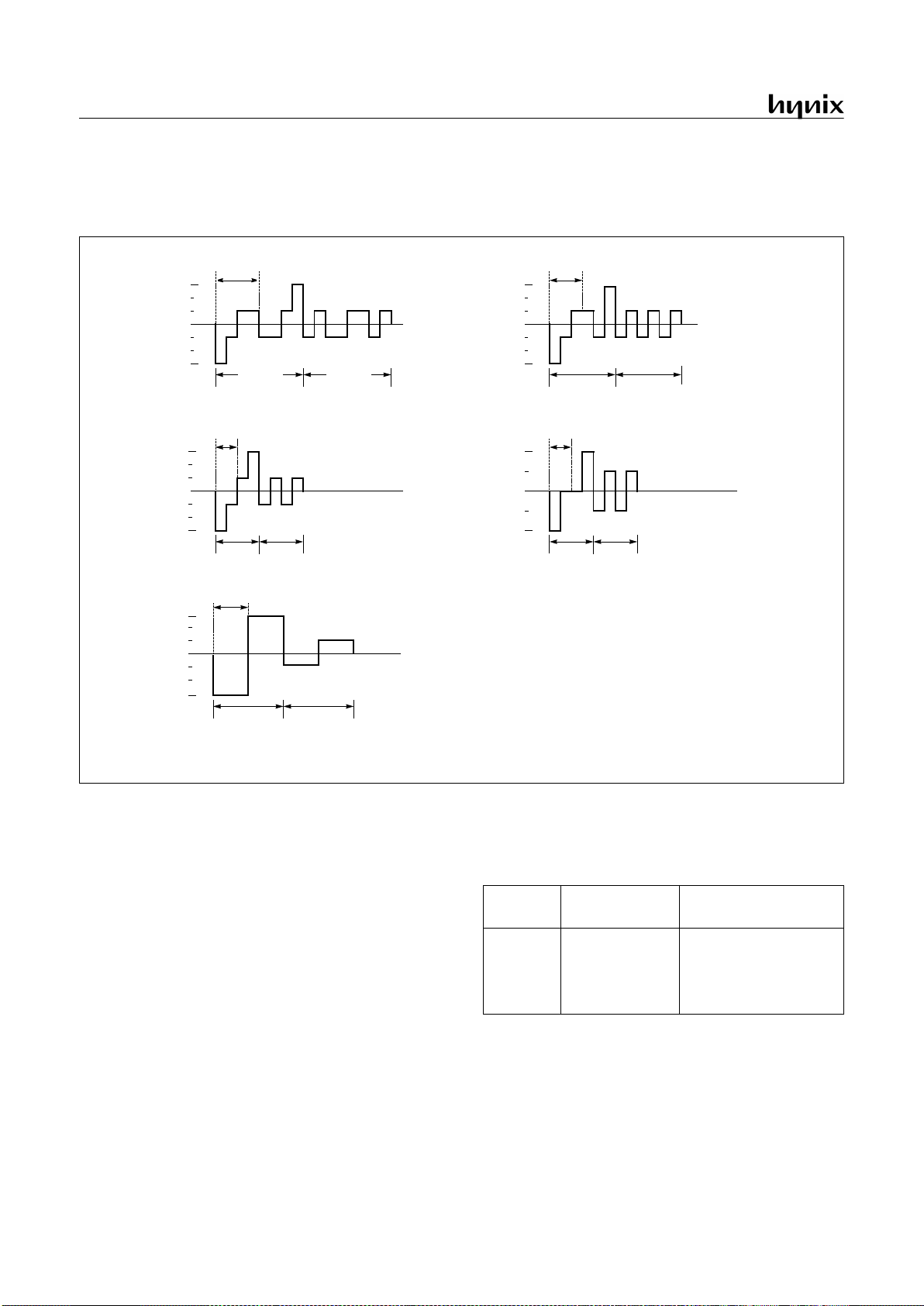
GMS81C7008/7016
72 APR., 2001 Ver 2.01
18.2 Duty and Bias Selection of LCD driver
5 kinds of driving methods can be selected by DTY (bits 3 and 2
of LCD Control Regist er and conne ction of VCL pin exte rnall y.
Figure 18-3 shows typical driving waveforms for LCD.).
Figure 18-3 LCD drive waveform (Voltage COM-SEG Pins)
18.3 Selecting Frame Frequency
Frame frequency is set to the base frequency as shown in the following Table 18-1.
The LCK[1:0] of LCR determines the frequen cy of COM signal
scanning of each segment output. The watch timer must be enabled when the LCD display is turned on. RESET clears the LCD
control register LCR values to logic zero. The LCD display can
continue to operate even during the SLEEP and STOP modes if a
sub-frequency clock is oscillate and used as clock source of LCD
driver.
.
VCL2
VCL1
VCL0
GND
-VCL0
-VCL1
-VCL2
1/f
F
Data “1”
(a) 1/4 duty, 1/3 bias
Data “0”
VCL2
VCL1
VCL0
GND
-VCL0
-VCL1
-VCL2
1/f
F
Data “1”
(b) 1/3 duty, 1/3 bias
Data “0”
1/f
F
Data “1” Data “0”
(c) 1/2 duty,1/3 bias
1/f
F
Data “1” Data “0”
VCL2
VCL1
VCL0
GND
-VCL0
-VCL1
-VCL2
(e) Static
Note: fF: LCD Frame Frequency
1/f
F
Data “1” Data “0”
VCL2
GND
-VCL0 = -VCL1
-VCL2
(d) 1/2 duty, 1/2 bias
VCL1 = VCL0
VCL2
VCL1
VCL0
GND
-VCL0
-VCL1
-VCL2
LCK[1:0] LCD clock
Frame Frequency (Hz)
(When f
SUB
= 32.768 kHz)
00
01
10
11
f
SUB
÷ 32
f
SUB
÷ 64
f
SUB
÷ 128
f
SUB
÷ 256
1024
512
256
128
Table 18-1 Setting of LCD Frame Frequency
Page 77

GMS81C7008/7016
APR., 2001 Ver 2.01 73
LCD Port Selection
Segment pins are also used for normal I/O pins. The LCD port selection register LPMR is used to set Rn pin for ordinary digital input. Refer to LPMR register as shown in Figure 18-2.
Bias Resistor
To operate LCD, built- in Bias resistor dividing V
DD
to V
SS
section into several stages generates necessary voltage.
The BTC (Bit 6 of LCR) switches Transistor supplying voltage to
serially connected Bias resistor. If it is ‘1’, it turns on, and if it is
‘0’, it turns off. The LCD driv e voltage (V
CL2
) is given by the dif -
ference in potential (V
DD-VCL2
) between pins VDD and V
CL2
.
Therefore, when the MCU operating vo ltage is 5V and LCD drive
voltage are the same, the Bias pin is connected to the V
CL2
pin as
shown in (a) of Figure 18-5.
Figure 18-4 Application Example of 5V LCD Panel
When require supply 3V output to the LCD, the voltage of V
CL2
becomes 3V as shown in Fig ure 18-5. Because VDD is down to
3V through internal 2R r e sistor.
The LCD light only when the difference in p oten tial be twe en th e
segment and comm on output is ±VCL, and turn off at all other
times. During reset, the power switc h of the LCD driver is tu rned
off automatically, shutting off the VCL voltage.
one frame
(at 1/4 duty, 1/3 bias)
COM0 pin
VCL1
VCL2
BIAS
BTC
V
DD
V
SS
(a) Internal, Static or 1/3 Bias
BTC = “1”
BRC = “1”
Internal Bias resistors
MCU Internal
VCL0
BRC
2R
R
R
R
BTC
V
DD
V
SS
(b) Internal, Static or 1/2 Bias
BTC = “1”
BRC = “1”
Two pins are connected
each other
Internal Bias resistors
MCU Internal
BRC
2R
R
R
R
Typ. R=65k
Ω
VCL1
VCL2
BIAS
VCL0
Short two pins
each other externally
VCL2=5V
VCL1=3.33V
VCL0=1.67V
VCL2=5V
VCL1=2.5V
VCL0=2.5V
Page 78

GMS81C7008/7016
74 APR., 2001 Ver 2.01
Figure 18-5 Application Example of 3V LCD Panel
Some user want to use external bias resisor instead of internal,
you can connect external resistor as shown in Figure 18-6. And
the external capacitors are may require d for stable display according to your system environment.
Figure 18-6 External Resistor
VCL1
VCL2
BIAS
BTC
VDD = 5V
V
SS
(a) Internal, Static or 1/3 Bias
BTC = “1”
BRC = “1”
Short two pins
externally
Internal Bias resistors
MCU Internal
VCL0
BRC
2R
R
R
R
Typ. R=65k
Ω
BTC
VDD = 5V
V
SS
(b) Internal, Static or 1/2 Bias
BTC = “1”
BRC = “1”
Internal Bias resistors
MCU Internal
BRC
2R
R
R
R
Typ. R=65k
Ω
VCL1
VCL2
BIAS
VCL0
VCL2=3V
VCL1=2V
VCL0=1V
VCL2=3V
VCL1=1.5V
VCL0=1.5V
VCL1
VCL2
BIAS
BTC
V
DD
V
SS
BTC = “0”
BRC = “0”
External circuit
Internal Bias resistors
MCU Internal
VCL0
BRC
2R
R
R
R
V
SS
V
DD
Adjust Contrast
Page 79

GMS81C7008/7016
APR., 2001 Ver 2.01 75
18.4 LCD Display Memory
Display data are stored to the display data area (address
100
H
-11AH) in the data memory.
The display data stored to the display data area are read automatically and sent to the LCD driver by the hardware.
The LCD driver generates the segment signals and common signals in accordance with the display data and drive
method.
Figure 18-7 LCD Display Memory
Therefore, display patterns can be changed by only overwriting the contents of the display data area with a program. The table look up instruction is mainly used for this
overwriting.
Figure 18-7 shows the correspondence between the display
data area and the SEG/COM pins. The LCD lights when
the display data is “1” and turn off when “0”.
The number of segment which c an be driven differs depending on the LCD drive method, therefore, the number
of display data area bits used to store the data also differs
(Refer to Figure 18-2). Consequently, data memory not
SEG0
SEG1
SEG2
SEG3
SEG4
SEG5
SEG6
SEG7
COM0
COM1
COM2
COM3
SEG8
SEG9
SEG10
SEG11
SEG12
SEG13
SEG14
SEG15
SEG16
SEG17
SEG18
SEG19
SEG20
SEG21
SEG22
SEG23
SEG24
SEG25
SEG26
01234567Bit
100
H
101
H
102
H
103
H
104
H
105
H
106
H
107
H
108
H
109
H
10A
H
10B
H
10C
H
10D
H
10E
H
10F
H
110
H
111
H
112
H
113
H
114
H
115
H
116
H
117
H
118
H
119
H
11A
H
Note:
The bit 4 to 7 of every byte are
reserved. Any read or write is not
effect.
Drive methods Bit 3 Bit 2 Bit 1 Bit 0
1/4 duty COM3 COM2 COM1 COM0
1/3 duty - COM2 COM1 COM0
1/2 duty - - COM1 COM0
Static
---
COM0
Table 18-2 The duty vs. COM port Configuration
Page 80

GMS81C7008/7016
76 APR., 2001 Ver 2.01
used to store display data and data memory for which th e
address are not connected to LCD can be used to store ordinary user’s processing data.
Blanking
Blanking is applied by setting LCDEN (bit 7 of LCR) to “0” and
turns off the LCD by outputting the non light operation level to
the COM pin. When settin g Fram e frequen cy or cha nging op erating mode, LCD display should be off before operation, to prevent
display flickering.
18.5 Control Method of LCD Driver
Initial Setting
Flow chart of initial setting is shown in Figure 18-8.
Example: When operating with 1/4 duty LCD using a
frame frequency of 512Hz.
.
Figure 18-8 Initial Setting of LCD Driver
Figure 18-9 Example of Connection COM & SEG
Display Data Setting
Normally, display data are kept permanently in the program memory and then stored at the display data area by
the table look-up instruction. This can be ex plained using
numerical display with 1/4 duty LCD as an example. The
COM and SEG connections to the LCD and display data
are the same as those shown is Figure 18-9. Programming
LDM LCR,#0101_0001B ;1/4duty, fF=512Hz
(f
SUB
= 32.768kHz)
:
SETG
LDM RPR,#1 ;Select LCD Memory
;area (Page 1 = address 1XXH)
LDX #0
C_LCD1: LDA #0 ;RAM Clear
;RAM(100H~11AH)
STA {X}+
CMPX #01BH
BNE C_LCD1
CLRG
:
:
SET1 LCR.5 ;Enable LCD display
:
:
Clear
LCD Display
Memory
Select Frame Frequency
Turn on LCD
Setting of LCD drive method
Initialize of display memory
Enable display
(Release of blanking)
SEG0
SEG1
COM3
COM0
COM1
COM2
Example: display “2”
1110
0101
****
****
100
H
101
H
3120bit 7 564
Note: * are don’t care.
Page 81

GMS81C7008/7016
APR., 2001 Ver 2.01 77
example for displaying character is shown below.
Note: When power on RESET, sub oscillatio n start up time
is required. Enable LCD display after sub oscillation is stabilized, or LCD may occur flicker at powe r on time shortly.
:
CLRG
LDX #DISPRAM
GOLCD: LDA {X}
TAY
LDA !FONT+Y ;LOAD FONT DATA
LDM RPR,#1 ;Set RPR = 1 to access LCD
SETG ;Set Page 1
LDX #0
STA {X}+ ;LOWER 4 BITS OF ACC. -> M(X)
XCN
STA {X} ;UPPER 4 BITS OF ACC. -> M(X+1)
CLRG ;Set Page = 0
:
:
FONT DB 1101_0111B ; “0”
DB 0000_0110B ; “1”
DB 1110_0011B ; “2”
DB 1010_0111B ; “3”
DB 0011_0110B ; “4”
DB 1011_0101B ; “5”
DB 1111_0101B ; “6”
DB 0000_0111B ; “7”
DB 1111_0111B ; “8”
DB 0011_0111B ; “9”
Font data
Write into the
LCD Memory
Page 82

GMS81C7008/7016
78 APR., 2001 Ver 2.01
19. WATCH / WATCHDOG TIMER
19.1 Watch Timer
The watch timer goes the clock continuously even during the
power saving m ode. When MCU is i n the Stop or Slee p mode,
MCU can wake up itself every 2Hz or 4Hz or 16Hz.
The watch timer consists of input clock selector, 14-bit binary
counter, interval selector and Watch Timer Mode Register
WTMR (address 0EF
H
). The WTMR is 5-bit read/write register
and shown in Figure 19-2. WTMR can select the clock input by
2 bits WTCK[1:0] and interval time sel ector by 2 bits WT IN[1:0]
and enable/disable bit. The WTEN bit is set to “1” timer start
counting. Input clocks can be selected among three different
source which are sub clock or divided main clock (f
XIN
÷128) or
main clock. For t he switc hing betwe en main a nd sub clock, rec-
ommend the oscillator 4.194304MHz as a main and 32.768kHz
as a sub. Because above main frequency is equal to 128 times of
sub frequency. Generally main clock (f
XIN
) at WTCK=10B is not
be used, it is just for test purpose in factory.
In the Stop Mod e, the m ain c l ock is st oppe d b ut sub c lo ck is os-
cillation continuous ly for watch c lock operation. Ou tput tim er interval can be selected and Watch Timer Interrupt is generated.
LDM IENL,#XXXX_X1XXB
EI
LDM WTMR,#0100_1000B
Figure 19-1 Block Diagram of Watchdog Timer
19.2 Watchdog Timer
The watchdog timer rapidly de tects the CPU m alfunctio n suc h as
endless looping caused by noise or the like, and resumes the CPU
to the normal state.
The watchdog time r signal for det ecting ma lfunction ca n be selected either a reset CPU or a interrupt request as you want .
When the watchdog timer is not being used for malfunction detection, it can be used as a ti mer to gene rat e an in terrupt at fixe d
intervals.
Watchdog Timer Control
Figure 19-2 shows the watchdog timer control register WDTR
(address 0DF
H
). The watchdog timer is automatically enabled
initially and watchdog output to reset CPU but clock input source
is disabled. To enable this function, you should write bit WTEN
of WTMR (address 0EF
H
) set to “1”.
The CPU malfunction is detected during setting of the detection
time, selecting of output, and clearing of the binary counter.
Clearing the 2-bit binary counter by bit WDCLR of WDTR is repeated within the detection time.
If the malfunction occurs for any cause, the watchdog timer output will become active from the binary co unters unless the binary
counter is cleared. At this time, when WDOM=1, a reset is generated, which d rives the RES ET
pin to low to reset the internal
hardware. When WDOM=0, a watchdog timer int errupt (WDTIF) is generated instead of Reset function. This interrup t can be
used general timer as us e r wa nt.
When main clock is select ed as cloc k input so urce on t he STOP
mode, clock input is stopped so the watchdog timer temporarily
stops counting. The other side, when sub clock is selected as
clock input s our ce on t he S TO P mo de , su b c loc k op er ates al way s
enable
Watch Timer interrupt
WTIF
0
1
14-bit Binary Counter
MUX
f
SXIN
f
XIN
÷128
f
XIN
f
W
f
SXIN
= 32.768 kHz
f
XIN
= 4.194304 MHz
Interval Selector
2Hz
4Hz
16Hz
2Hz
4Hz
8Hz
16Hz
2-bit Binary Counter
WDCK[1:0]
WTIN[1:0]
WTCK[1:0]
WDOE[0DFH]
R34/WDTO
clear
0: Stop
1: Clear and start
WDCLR
WDTIF
to RESET CPU
Watchdog Timer Interrupt
overflow
WDEN
WDOM
00
01
10
00 01 10 11
000110
enable
0
1
WTEN
MUX
When
Page 83

GMS81C7008/7016
APR., 2001 Ver 2.01 79
so the watchdog timer works continuously.
Figure 19-2 WTMR, WDTR: Watch Timer and Watchdog Timer Data Register
Example: Sets the watchdog timer detection time to 1 sec at 4.19MHz, 32.768kHz
Enable and Disable Watchdog
Watchdog timer is enable d by se tting W DEN (bi t 4 in CKCT LR)
to “1”. WDEN is initialized to “1” during reset and it should be
clear to “0” disable.
Example: Enables watchdog timer for Reset
:
LDM WTMR,#0100_XXXXB;
WTEN
← 1
LDM WDTR,#00X1_XX11B;
WDEN
← 1
:
The watchdog timer is di sabl ed by clearin g eith er bi t 4 (WDEN)
of WDTR or bit 6 (WTEN) of WTMR. The watchdog timer is
halted in STOP mode and restarts auto matically after STOP mode
is released.
Clearing 2-bit binary counter of the Watchdog
timer
The watchdog timer count the clock source as 14-bit binary
INITIAL VALUE: -0--_0000
B
ADDRESS: 0EF
H
WTMR
-
-
WTEN WTIN1 WTIN0
-R/WR/W R/W-R/W R/W
--
WTCK1WTCK0
Clock source selection
00: Sub clock
01: Main clock (f
XIN
÷
128)
10: Main clock (test purpose in factory)
11: -
Watch timer interrupt interval selection
00: 16Hz
01: 4Hz
10: 2Hz
11: -
Watch Timer count enable
0: Disable
1: Enable
INITIAL VALUE: --01_0010
B
ADDRESS: 0DF
H
WDTR
-
WDOE WDCK1 WDCK0
R/WR/W R/W--R/W
-
WDEN WDOM
WDCLR
Watchdog timer interrupt interval selection
00: 2 sec.
01: 1 sec.
10: 0.5 sec.
11: 0.25 sec.
R34/WDTO selection
0: R34 port
1: WDTO
port
R/W R/W
Clear bit
0: Normal operation
1: Clear and starts counting
When
f
SXIN
= 32.768kHz
f
XIN
= 4.19MHz
Output Mode
0: Interrupt request
1: Reset CPU
Watchdog Timer count enab le
0: Disable
1: Enable
When
f
SXIN
= 32.768kHz
f
XIN
= 4.19MHz
LDM WTMR,#0100_1000B ;
Select sub clock as an input source
LDM WDTR,#0001_0111B
SET1 WDCLR ;
Clear counter
:
:
:
:
SET1 WDCLR ;
Clear counter
:
:
:
:
SET1 WDCLR ;
Clear counter
Within 0.75 sec.
Within 0.75 sec.
Page 84

GMS81C7008/7016
80 APR., 2001 Ver 2.01
counter which is free run can not be cleared. The watchdog timer
has 2-bit binary counter. It is incremented by 14-bit binary
counter match as shown in Figure 19-1. Interrupt request flag or
Reset signal are generated by overflow 2-bit binary counte r.
During normal operation in the software, 2-bit binary counter
should be cleared by bit WDCLR of WDTR within watchdog
timer overflow.
The time of clearing must be within 3 times of 14-bit binary
counter inte rval as shown in Figure 19-3.
The worst case, watchdog time is just 3 times of 14-bit counter.
Figure 19-3 Watchdog timer Timing
If the watchdog timer output becomes active, a reset is gen erated,
which drives th e RESET
pin low to reset the internal hardware.
The main clock oscillator also turns on when a watchdog timer reset is generated in sub clock mode.
14-bit binary
2-bit binary
WDTIF interrupt
Write WDCLR = 1 at this point
10
Counter
Clear
n
counter
R34/WDTO pin
reset
0
1
1FFE
~
~
~
~
1FFF
counter
0 23
01
1FFE 1FFF
01
1FFE 1FFF
~
~
~
~
01
1FFE 1FFF
2
222
~
~
~
~
8 osc.
(2us at f
XIN
=4.19MHz)
Even if user set to 1 sec.,
When WDTR = 0011_0111B
worst case 0.75 second
Page 85
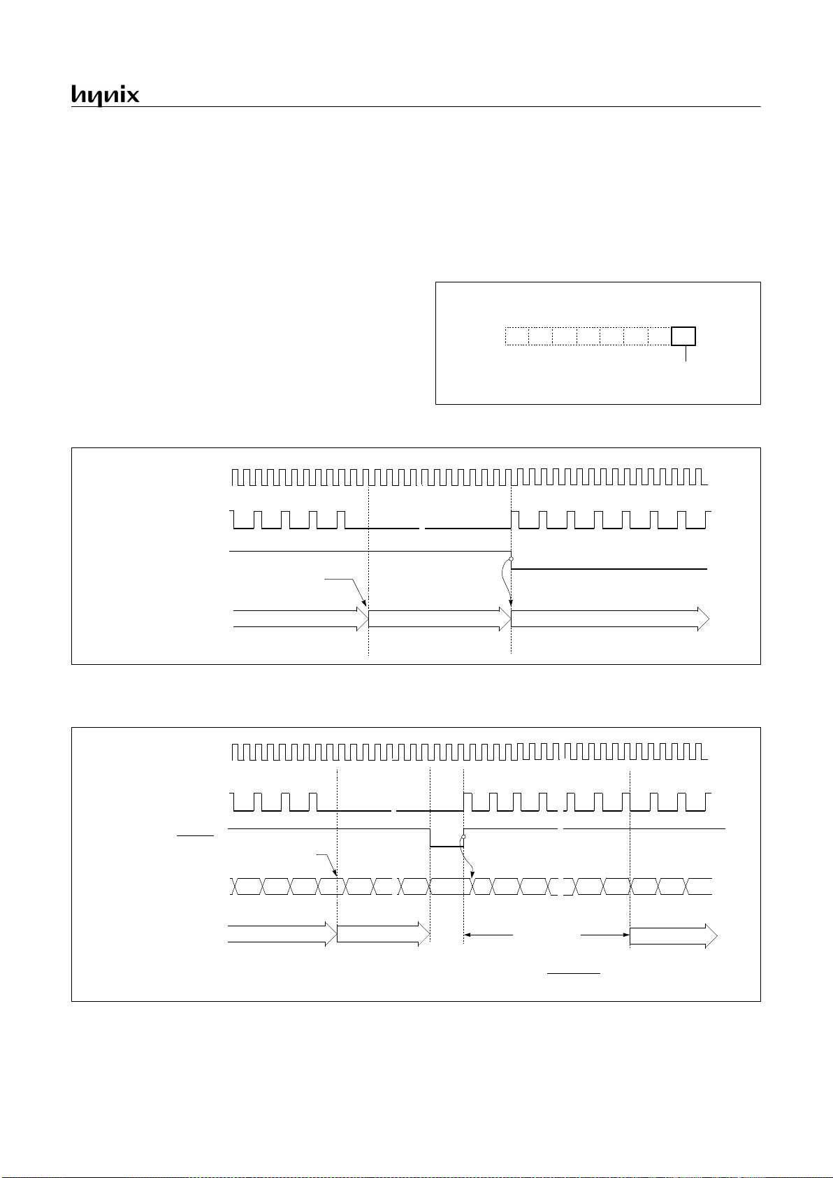
GMS81C7008/7016
APR., 2001 Ver 2.01 81
20. POWER DOWN OPERATION
The GMS81C7008/16 has t wo power-down modes. In power down mode, power consumption is reduced considerably that in
Battery operation Battery life can be extended a lot.
Sleep mode is entered by setting bit 0 of Sleep Mode Register, and STOP Mode is entered by STOP instruction.
20.1 SLEEP Mode
In this mode, the internal oscillation circuits remain active.
Oscillation continues and peripherals are operate normally but
CPU stops. Movement of all Peripherals is shown in Table 20- 1.
Sleep mode is entered by setting bit 0 of SMR (address 0D E
H
).
It is released by RESET or interrupt. To be release by interrupt,
interrupt should be enabled before Sleep mode.
Figure 20-1 SLEEP Mode Register
Figure 20-2 Sleep Mode Release Timing by External Interrupt
.
Figure 20-3 SLEEP Mode Release Timing by RESET pin
Sleep Mode Register
SMR
ADDRESS : 0DE
H
RESET VALUE : -------0
0: Release Sleep Mode
1: Enter Sleep Mode
W
Oscillator
Normal Operation Stand-by Mode Normal Operation
Interrupt
Internal CPU Clock
Release
Set bit 0 of SMR
(XIN or SXIN pin)
~
~
~
~
Oscillator
(X
IN
or SXIN pin)
0
BIT Counter
1
FE
FF
0
12
~
~
tST = 62.5ms
~
~
~
~
RESET
Internal CPU Clock
Clear & Start
~
~
~
~
Normal Operation Sleep Mode
Normal Operation
Release
Set bit 0 of SMR
~
~
~
~
~
~
at 4.19MHz by hardware
~
~
2
t
ST
= x 256
f
MAIN
÷1024
1
Page 86

GMS81C7008/7016
82 APR., 2001 Ver 2.01
20.2 STOP Mode
For applications where power consumption is a critical
factor, device provides reduced power of STOP.
Start The Stop Operation
An instruction that STOP causes to be the last instruct ion
is executed before going into the STOP m ode. In the Stop
mode, the on-chip main-frequency oscillator is stopped.
With the clock frozen, all functions are stopped, but the onchip RAM and Control registers are held. The port pins
output the values held by their respectiv e port data register,
the port direction registers. The status of peripherals during
Stop mode is shown below.
Note: Since the XIN pin is connected internally to GND to
avoid current leakage due to the crystal oscillator in STOP
mode, do not use STOP instruction when an external clock
is used as the main system clock.
In the Stop mode of operation, VDD can be reduced to mi n imi ze
power consumption. Be careful, however, that V
DD
is not re-
duced before the Stop mode is invoked, and that V
DD
is restored
to its normal operating level before the Stop mode is terminated.
The reset should not be activated before VDD is restored to its
normal operatin g level, a nd must be he ld active long enou gh to
allow the oscillator to restart and stabilize.
And after STOP instruction, at least two or more NOP instruction
should be written as shown in example below.
Example)
LDM CKCTLR,#0EB ;32.8ms
; LDM CKCTLR,#0FB ;65.5ms
STOP
NOP
NOP
:
The Interval Timer Register CKCTLR shou ld be in iti ali zed (0 F
H
or 0EH) by software in order that oscillation stabilization time
should be longer than 20ms before STOP mode.
Release the STOP mode
The exit from STOP mode is using hardware reset or external interrupt, watch timer, key scan or timer/counter.
To release STOP mode, corresponding interru pt should be
enabled before STOP mode.
Specially as a clock source of Timer/Event counter, EC0 or EC2
pin can release it by Timer/Event counterInterrupt request
Reset redefines a ll the co ntrol regi sters but does not change the
on-chip RAM. External interrupts allow both on-chip RAM and
Control registers to retain their values.
Start-up is performed to acquire the time for stabilizing oscillation. During the start-up, the internal op erati on s are all stopp ed.
Peripheral STOP Mode SLEEP Mode
CPU All CPU operations are disabled All CPU operations are disabled
RAM Retain Retain
LCD driver LCD driver operates continuously LCD driver operates continuously
Basic Interval Timer Halted BIT operates continuously
Timer/Event counter
Halted (Only when the Event counter mode
is enabled, Timer operates normally)
Timer/Event counter operates continuously
Watch Timer Watch Timer operates continuously Watch Timer operates continuously
Main-oscillation Stop (X
IN
pin = “L”, X
OUT
pin = ”L”) Oscillation
Sub-oscillation Oscillation Oscillation
I/O ports R e tain Retain
Control Registers Retain Retain
Release method
RESET, Key Scan interrupt, SIO interrupt,
Watch Timer interrupt, Timer interrupt
(EC0,2), External interrupt
RESET, All interrupts
Table 20-1 Peripheral Operation during Power Down Mode
Page 87

GMS81C7008/7016
APR., 2001 Ver 2.01 83
Figure 20-4 STOP Mode Release Timing by External Interrupt
Figure 20-5 STOP Mode Release Timing by RESET
Minimizing Current Consumption
The Stop mode is designed to reduce power consumption.
To minimize current drawn during Stop mode, the user
should turn-off output drivers that are sourcing or sinking
current, if it is practical.
Note: In the STOP operation, the power dissipation associated with the os cillato r and th e inter nal hard ware is lowered; however, the power dissipation associated with the
pin interface (depending on the external circuitry and program) is not directly determined by the hardware operation
of the STOP feature. Th is point sh ould be little c urrent flows
when the input level is stable at the power voltage level
(V
DD/VSS
); however, when the input level becomes higher
than the power voltage level (by approximately 0.3V), a current begins to flow. Therefore, if cutting off the output transistor at an I/O port puts t he pin signal i nto the highimpedance state, a curre nt flow ac ross the por ts i nput tran sistor, requiring it to fix the level by pull-up or other means.
Before executing Stop instruction, Basic Interval Timer must be set
Oscillator
(X
IN
pin)
~
~
n
0
BIT Counter
n+1 n+2
n+3
~
~
Normal Operation Stop Operation Normal Operation
1
FE
FF
0
12
~
~
~
~
~
~
tST > 20ms
~
~
~
~
External Interrupt
Internal Clock
Clear
STOP Instruction
Executed
~
~
~
~
~
~
properly by software to get stabilization time which is longer than 20ms.
by software
~
~
Oscillator
(X
IN
pin)
~
~
n
0
BIT Counter
n+1 n+2
n+3
~
~
Normal Operation
Stop Operation Normal Operation
1
FE
FF
0
12
~
~
~
~
~
~
tST > 62.5ms
Internal Clock
Clear
STOP Instruction
Executed
~
~
~
~
~
~
at 4.19MHz by hardware
~
~
RESET
n+2
t
ST
= x 256
f
MAIN
÷1024
1
~
~
~
~
Page 88

GMS81C7008/7016
84 APR., 2001 Ver 2.01
It should be set properly that current flow through port doesn't exist.
First consider the setting to input mode. Be sure that there is no
current flow after considering its relationship with external circuit. In input mode, the pin impeda nce viewing from ext ernal
MCU is very high that the current doesn’t fl ow.
But input voltage level should be V
SS
or VDD. Be careful that if
unspecified voltage, i.e. if un-firmed voltage level (not V
SS
or
V
DD
) is applied to input p in, there can be little curren t (max. 1mA
at around 2V) flow.
If it is not appropriate to set as an input mode, then set to output
mode considering there is no curren t flow. Setting to High or Low
is decided considering its relationship with external circuit. For
example, if there is externa l pull-up re sistor then it i s set to o utput
mode, i.e. to High, and if there is external pull-down register, it is
set to low.
Figure 20-6 Application Example of Unused Input Port
Figure 20-7 Application Example of Unused Output Port
INPUT PIN
V
DD
GND
i
V
DD
X
Weak pull-up current flows
V
DD
internal
pull-up
INPUT PIN
i
V
DD
X
Very weak current flows
V
DD
O
O
OPEN
OPEN
i=0
O
i=0
O
GND
When port is configure as an input, input level should
be closed to 0V or 5V to avoid power consumption.
OUTPUT PIN
GND
i
In the left case, much current flows from port to GND.
X
ON
OFF
OUTPUT PIN
GND
i
In the left case, Tr. base current flows from port to GND.
i=0
X
OFF
ON
V
DD
L
ON
OFF
OPEN
GND
V
DD
L
ON
OFF
To avoid power consumption, there should be low output
ON
OFF
O
O
V
DD
O
to the port .
Page 89

GMS81C7008/7016
APR., 2001 Ver 2.01 85
21. OSCILLATOR CIRCUIT
The GMS81C7008/16 has two oscilla tion circ uits internall y. X
IN
and X
OUT
are input an d ou tpu t for main frequ en c y and SXIN and
SX
OUT
are input and output for s ub frequenc y, respective ly, inverting amplifier which can be configured for being used as an
on-chip oscillator, as shown in Fig ure 21-1. To use RC oscillation
instead of crystal, user should check mark on the "A. MASK ORDER SHEET" o n page i of the a ppend ix of this manua l. Howe ver
in the OTP device, when the progr amm ing RC os cilla tio n c an be
selected or not into the co nfigura tion bi t. For m ore deta il, refer to
"24.1 OTP Programming" on page 89.
Note: When using the sub clock oscillation, connect a resistor in series with R which is shown as below fi gure.
In order to reduce the power consumption, the sub clock
oscillator employs a low amplification fact or circuit. Because of this, the sub clock oscillator is more sensitive to
noise than the main system clock oscillator.
Figure 21-1 Oscillation Circuit
Oscillation circuit is designed to be used either with a ceram ic
resonator or crystal oscillator. Since each crystal and ceramic resonator have their own characteris tics, the user should consult the
crystal manufacturer for appropriate values of external components.
Oscillation circuit is designed to be used either with a ceram ic
resonator or crystal oscillator. Since each crystal and ceramic resonator have their own characteris tics, the user should consult the
crystal manufacturer for appropriate values of external components. In addition, see Figure 21-2 for the layout of the crystal.
Note: Minimize the wiring length. Do not allow the wiring to
intersect with other signa l cond uctors . Do not all ow the wiring to come near changing high current. Set the potential of
the grounding position of the oscillator capacitor to that of
V
SS
. Do not ground it to any g round pattern where high cur-
rent is present. Do not fetch signals from the oscillator.
Figure 21-2 Recommend Layout of Oscillator PCB
circuit
X
OUT
X
IN
V
SS
Recommend
C1,C2 = 20pF
C1
C2
X
OUT
X
IN
External Clock
Open
X
OUT
X
IN
External Oscillator RC Oscillator
(mask option)
Crystal or Ceramic Oscillator
SX
OUT
SX
IN
V
SS
Recommend
C1,C2 = 30pF±5pF
C1
C2
32.768kHz
4.19MHz
Crystal Oscillator
Ceramic Resonator
C1,C2 = 30pF
Refer to AC Characteristics
For selection R value,
R
EXT
R
R= 47kΩ±5k
Ω
X
OUT
X
IN
Page 90

GMS81C7008/7016
86 APR., 2001 Ver 2.01
22. RESET
The GMS81C7008/16 has two types of reset generation procedures; one is an external reset input, the ot her is a watch- dog timer reset. Table 22-1 shows on-chip hardware initialization by
reset action.
Figure 22-1 Simple Power-on-Reset Circuit.
22.1 External Reset Input
The reset input is the RESET pin, which is the inp ut to a Sch mitt
Trigger. A reset in accomplished by holding the RESET pin low
for at least 8 oscillator periods, with in the operating voltage range
and oscillation stable, it is applie d, and the inte rnal state is initia lized. After reset, 64 ms (at 4 MHz) add with 7 os cillato r periods
are required to start execution as shown in Figure 22-2.
Internal RAM is not affected by reset. When V
DD
is turned on,
the RAM content is indeterminate. Therefore, this RAM should
be initialized before read or tested it.
When the RESET pin inpu t goes to hig h, the reset op eration is re -
leased and the program execution starts at the vector address
stored at addresses FFFE
H
- FFFFH.
A connection for simple power-on-reset is shown in Figure .
Figure 22-2 Timing Diagram after RESET
22.2 Watchdog Timer Reset
Refer to “18. LCD DRIVER” on page 70.
7036P
V
CC
10uF
+
10k
Ω
to the RESET pin
On-chip Hardware Initial Value
Program counter (PC)
(FFFF
H
) - (FFFEH)
G-flag (G) 0
Operation mode Main operating mode
Peripheral clock On
Watchdog timer
Disable (Because the Watch
timer is disabled)
Control registers
Refer to Table 8-1 on
page 25
Low voltage detector Enable
Table 22-1 Initializing Internal Status by Reset Action
MAIN PROGRAM
Oscillator
(X
IN
pin)
?
?
FFFE FFFF
Stabilization Time
t
ST
= 62.5mS at 4.19MHz
RESET
ADDRESS
DATA
1 2 3 4 5 6 7
??
Start
?
??
FE?ADL
ADH
OP
BUS
BUS
RESET Process Step
~
~
~
~
~
~
~
~
~
~
~
~
t
ST
= x 256
f
MAIN
÷1024
1
Page 91

GMS81C7008/7016
APR., 2001 Ver 2.01 87
23. POWER FAIL PROCESSOR
The GMS81C7008/16 has an on-chip low voltage detection circuitry to detect the V
DD
voltage. A configuration register, LVDR
(address 0FB
H
), can enable or disable t he l ow voltage detect cir-
cuitry. Whenever V
DD
falls close to or below 2.2V, the LVD0 is
just set to “1”, and if it recovering 3.4V, LVD0 is held to “1”. If
VDD falls below around 3.4V range, the low voltage situation
may reset the MCU or freeze the clock according to setting of bit
5 (LVDM) of LVDR . The bit 4 LVD1 function is same with
LVD0 except different voltage level 2.1 V . The dete c tion volta ge
is varied very little. See "7.3 DC Electrical Characteristic s" on
page 11 for more detail voltage level.
In the in-circuit emulat or, po wer fail fu nction is not im plement ed
and user may not use it. Therefore, after completed development
of user program , th is fun c tio n m a y be experimented or e va lu at ed
using by OTP.
When power fail certainly occur the MCU was re set, program notify this Reset circumstance cause by LVD functio n. So, doe s not
erase the all RAM content s and opera tes subseq uently as shown
in Figure .
Figure 23-1 Low Voltage Detector Register
76543210
LVDE
INITIAL VALUE: 00
H
ADDRESS: 0FB
H
LVDR
R/W R/W R/W
LVD1
Operation Mode
0: Clock freeze
1: Reset
Enable / Disable Flag
0: Disable
1: Enable
LVDS LVD0
Power Fail Voltage Selection
0: 3.4V
1: 2.1V
R/W
LVDM
VDD Detection Flag 1
0: Above 3.4V
1: Below 3.4V
VDD Detection Flag 2
0: Above 2.1V
1: Below 2.1V
Figure 23-2 Example S/W of RESET by Power fail
FUNTION
EXECUTION
INITIALIZE RAM DATA
LVD0 =1
NO
RESET VECTOR
INITIALIZE ALL PORTS
INITIALIZE REGISTERS
RAM CLEAR
YES
Skip the initial routine when
the Reset cause from power fail.
Page 92

GMS81C7008/7016
88 APR., 2001 Ver 2.01
Figure 23-3 Power Fail Processor Situations
Internal
RESET
Internal
RESET
Internal
RESET
V
DD
V
DD
V
DD
LVDVDDMAX
LVDV
DD
MIN
LVDV
DD
MAX
LVDV
DD
MIN
LVDV
DD
MAX
LVDV
DD
MIN
64mS
64mS
t <64mS
64mS
When LVDM = 1
Page 93

GMS81C7008/7016
APR., 2001 Ver 2.01 89
24. DEVELOPMENT TOOLS
24.1 OTP Programming
The GMS87C7016 is OTP (One Time Programmable) type microcontrollers. Its internal user memory is constructed with
EPROM (Electrically Programmable Read Only Memory).
The OTP microcontroller is generally used for chip evaluation,
first production, small amount production, fast mass production,
etc.
Blank OTP’s internal EPROM is filled by 00H, not FFH.
Note: In any case, you have to use the *.OTP file for programming, not the * .HEX file. After assembl e the source
program, both OTP and HEX fi le are generated b y automatically. The HEX file is used during program emulation on
the emulator.
How to Program
To program the OTP devices, user should use HEI own programmer. Ask to HEI sales part for purchasing or more detail.
Programmer:
CHOICE-SIGMA
(Single type)
CHOICE-GNAG4
(4-gang type)
Socket adapter:87C70XX-64SD (for 64SDIP)
87C70XX-64QF (for 64MQFP)
The CHOICE-SIGMA is a HEI Universal Single Programmer for
all of HEI OTP devices, also the CHOICE-GANG4 can program
four OTPs at once.
Programming Procedure
1. Select device GMS87C7016 as you want.
2. Load the *.OTP file from the PC to Programmer. The
file is composed of Motorola-S1 format.
3. Set the programming address range as below table.
4. Mount the socket adapter on the programmer.
5. Set the configuration bytes as your needs.
6. Start program/verify.
Select the option for Program Lock and RC oscillation
Except th e user pr ogram memor y C000H~FFFFH, there is configuration byte (address 707F
H
) for the selection of program lock
and RC oscillation. The configuration byte of OTP is shown as
Figure 24-1. It could be served when user use the OTP programmer (Choice-Sigma or Choice-Gang4).
Figure 24-1 The OTP Configuration Byte
87C70XX-64SD
87C70XX-64QF
87C71XX-52SD
ADDRESS: 707F
H
76543210
OTP Configuration Byte
LOCK RC
0: Crystal or Resonator
1: External RC Oscillator
0: Allow code read out
1: Not allow code read out
Lock bit
Oscillation Option
Page 94

GMS81C7008/7016
90 APR., 2001 Ver 2.01
24.2 Emulator EVA. Board Setting
*1'
9&/4
9/&'&
&%
*1'
11&1
5(0287
+721(',
*1'
569
567
554
556
558
55:
549
547
545
543
539
537
535
533
565
563
.89
32:(5
581
6723
6/((3
CHOICE-Dr. EVA 81C51/81C7x B/D Rev 1.1 S/N. ---------------
-B86(5%
5(6(7
-B86(5$
9B86(5
;4#+26&,
;5
25(6(7
;287
/&'B9GG
9/&'&
6(*79
6(*77
6(*75
6(*73
6(*6;
95(*
&2042669
&2062667
6(*65
6(*63
6(*5;
6(*59
6(*57
6(*55
6(*53
6(*4;
6(*49
6(*47
6(*45
6(*43
6(*;
6(*9
6(*7
6(*5
6(*3
6(*7:
6(*78
6(*76
6(*74
6(*6<
6(*6:
&203
&2052668
6(*66
6(*64
6(*5<
6(*5:
6(*58
6(*56
6(*54
6(*4<
6(*4:
6(*48
6(*46
6(*44
6(*<
6(*:
6(*8
6(*6
6(*4
*1'
9&/3
9&/5
&$
*1'
28B567
8B;287
*1'
56:
568
553
555
557
559
54:
548
546
544
53:
538
536
534
566
564
.89
-B86(5%
-B86(5$
123456781
2
ONOFF
SW4
SW5
SW2
2 1
ONOFF
SW1
6XSSO\#.89#+PD[1#533P$,
VR1
+5V
External oscillator
socket
Page 95

GMS81C7008/7016
APR., 2001 Ver 2.01 91
DIP Switch and VR Setting
Before execute the user program, keep i n your mind the below configuratio n
DIP S/W, VR Description ON/OFF Setting
SW1 - Emulator Reset Switch. Reset the Emulator. Reset the Emulator.
SW2
1
Pod RESET pin configuration
Normally
OFF
.
EVA. chip can be reset by external
user target board.
ON
: Reset is available by either
user target system board or Emulator RESET switch.
OFF
: Reset the MCU by Emulator
RESET switch. Does not work from
user target board.
2
Pod XOUT pin configuration
Normally
OFF
.
MCU XOUT pin is disconnected
internally in the Emulator. Some circumstance user may connect this
circuit.
ON
: Output XOUT signal
OFF
: Disconnect circuit
SW4
1
2
3
External Bias Resistors Connection
Must be ON position.
It serves the external bias resistors.
If this switches are turned off, LCD
bias voltage does not supplied,
floated because there are no internal bias resistors an d bias Tr. ins ide
the Emulator.
4
56LCD Voltage doubling circuit.
Must be
OFF
position.
It is reserved for the GMS81C5108.
7 Select the Stack Page.
Must be ON position.
This switch select the Stack page 0
(off) or page 1 (on).
ON
: For the 81C7XXX
OFF
: For the GMS81C5108
8
81Cx detect the VDD voltage but Emulator can not do because
Emulator can not operate if V
DD
is below normal opr. voltage
(5V), This switch serves LVD environment through the applying
0V to LVD pin of EVA. chip during 5V normal operation.
Position ON during normal operation.
ON
: Normal operation
OFF
: Force to detect the LVD, refe r
to "23. POWER FAIL PROCESSOR" on page 87.
SW2-1
RESET pin
EVA.
Chip
SW2-2
XOUT pin
EVA.
Chip
Oscillator
VCL1
VCL2
BIAS
External Resistor
EVA. Ch ip Interna l
VCL0
V
SS
V
DD
Adjust Contrast
SW4-1
SW4-2
SW4-3
0.47uF × 3
10kΩ × 3
and Capacitor
VR1 50k
Ω
SW4
SW4-8
V
DD
EVA.
Chip
LVD pin
Page 96

GMS81C7008/7016
92 APR., 2001 Ver 2.01
SW5
1 Internal power supply to sub-oscillation circuit. Must be ON position.
2 Reserved for other purpose. Must be
OFF
position.
VR1 -
Adjust the LCD contrast. It supply bias voltage and adjust the
VCL2 voltage.
Adjust the proper pos ition as well as
LCD display good.
VR2 - Reserved for other purpose. Don’t care.
DIP S/W, VR Description ON/OFF Setting
VCL1
VCL2
BIAS
External Resistor
EVA. Ch ip Interna l
VCL0
V
SS
V
DD
Adjust Contrast
SW4-1
SW4-2
SW4-3
0.47uF × 3
10kΩ × 3
and Capacitor
VR1
50k
Ω
Page 97

APPENDIX
Page 98

A. MASK ORDER SHEET
1. Customer Information
Company Name
2. Device Information
3. Marking Specification
4. Delivery Schedule
Customer Sample
Date
YYYY MM DD
Risk Order
YYYY MM DD
Quantity
Hynix Confirmation
Application
Order Date
YYYY MM DD
Tel:
Fax:
Name &
Signature:
Package
64SDIP 64MQFP
5. ROM Code Verification
Verification Date:
YYYY MM DD
Approval Date:
YYYY MM DD
Ple a se co n firm o ur v e rificatio n da ta .
I agree with your verification data and confirm
you to m ake m ask s et.
Check Sum:
Tel:
Fax:
Name &
Signature:
Tel:
Fax:
Name &
Signature:
C000
H
E000
H
FFFF
H
.OTP file data
DFFF
H
Mask Data
Internet
File Name: ( .OTP)
(Please check mark into )
pcs
pcs
Check Sum: ( )
Customer should write inside thick line box.
This box is written after “5.Verification”.
RC OSC Opt.
Crystal
RC
GMS81C7016 (16K ROM)
GMS81C7008 (8K ROM)
ROM Size
8K 16K
YYWW
KOREA
Customer’s logo
Customer logo is not required.
YYWW
KOREA
GMS81C70
Customer’s part number
If the customer logo must be used in the special mark, please submit a clean original of the logo.
08 or 16
E-mail:
E-mail:
01-APR-2001
MASK ORDER & VERIFICATION SHEET
GMS81C7008
-LA
GMS81C7016
-LA
GMS81C70
-LA
Lot Number
Hynix ROM Code
Number
Page 99

GMS81C71XX LCD MCU APPENDIX
APR. 2001 Ver 2.01 ii
B. INSTRUCTION
B.1 Terminology List
Terminology Description
A Accumulator
X X - register
Y Y - register
PSW Program Status Word
#imm 8-bit Immediate data
dp Direct Page Offset Address
!abs Absolute Address
[ ] Indirect expression
{ } Register Indirect expression
{ }+ Register Indirect expression, after that, Register auto-increment
.bit Bit Position
A.bit Bit Position of Accumulator
dp.bit Bit Position of Direct Page Memory
M.bit
Bit Position of Memory Data (000
H
~0FFFH)
rel Relative Addressing Data
upage
U-page (0FF00H~0FFFFH) Offset Address
n Table CALL Number (0~15)
+ Addition
x
Upper Nibble Expression in Opcode
y
Upper Nibble Expression in Opcode
−
Subtraction
×
Multiplication
/ Division
( ) Contents Expression
∧
AND
∨
OR
⊕
Exclusive OR
~NOT
←
Assignment / Transfer / Shift Left
→
Shift Right
↔
Exchange
= Equal
≠
Not Equal
0
Bit Position
1
Bit Position
Page 100

GMS81C71XX LCD MCU APPENDIX
iii APR. 2001 Ver 2.01
B.2 Instruction Map
LOW
HIGH
0000000000010100010020001103001000400101050011006001110701000080100109010100A010110B011000C011010D011100E01111
0F
000 -
SET1
dp.bit
BBS
A.bit,rel
BBS
dp.bit,rel
ADC
#imm
ADCdpADC
dp+X
ADC
!abs
ASLAASLdpTCALL0SETA1
.bit
BITdpPOPAPUSH
A
BRK
001 CLRC
SBC
#imm
SBCdpSBC
dp+X
SBC
!abs
ROLAROLdpTCALL2CLRA1
.bit
COMdpPOPXPUSHXBRA
rel
010 CLRG
CMP
#imm
CMPdpCMP
dp+X
CMP
!abs
LSRALSRdpTCALL4NOT1
M.bit
TSTdpPOPYPUSHYPCALL
Upage
011 DI
OR
#immORdpORdp+XOR!abs
RORARORdpTCALL6OR1
OR1B
CMPXdpPOP
PSW
PUSH
PSW
RET
100 CLRV
AND
#imm
ANDdpAND
dp+X
AND
!abs
INCAINCdpTCALL8AND1
AND1B
CMPYdpCBNE
dp+X
TXSP
INC
X
101 SETC
EOR
#imm
EORdpEOR
dp+X
EOR
!abs
DECADECdpTCALL10EOR1
EOR1B
DBNEdpXMA
dp+X
TSPX
DEC
X
110 SETG
LDA
#imm
LDAdpLDA
dp+X
LDA
!abs
TXA
LDYdpTCALL12LDC
LDCB
LDXdpLDX
dp+Y
XCN DAS
111 EI
LDM
dp,#imm
STAdpSTA
dp+X
STA
!abs
TAX
STYdpTCALL14STC
M.bit
STXdpSTX
dp+Y
XAX STOP
LOW
HIGH
1000010100011110010121001113101001410101151011016101111711000181100119110101A110111B111001C111011D111101E11111
1F
000
BPL
rel
CLR1
dp.bit
BBC
A.bit,rel
BBC
dp.bit,rel
ADC
{X}
ADC
!abs+Y
ADC
[dp+X]
ADC
[dp]+Y
ASL
!abs
ASL
dp+X
TCALL1JMP
!abs
BIT
!abs
ADDWdpLDX
#imm
JMP
[!abs]
001
BVC
rel
SBC
{X}
SBC
!abs+Y
SBC
[dp+X]
SBC
[dp]+Y
ROL
!abs
ROL
dp+X
TCALL3CALL
!abs
TEST
!abs
SUBWdpLDY
#imm
JMP
[dp]
010
BCC
rel
CMP
{X}
CMP
!abs+Y
CMP
[dp+X]
CMP
[dp]+Y
LSR
!abs
LSR
dp+X
TCALL
5
MUL
TCLR1
!abs
CMPWdpCMPX
#imm
CALL
[dp]
011
BNE
rel
OR
{X}OR!abs+YOR[dp+X]OR[dp]+Y
ROR
!abs
ROR
dp+X
TCALL7DBNEYCMPX
!abs
LDYAdpCMPY
#imm
RETI
100
BMI
rel
AND
{X}
AND
!abs+Y
AND
[dp+X]
AND
[dp]+Y
INC
!abs
INC
dp+X
TCALL
9
DIV
CMPY
!abs
INCWdpINC
Y
TAY
101
BVS
rel
EOR
{X}
EOR
!abs+Y
EOR
[dp+X]
EOR
[dp]+Y
DEC
!abs
DEC
dp+X
TCALL11XMA
{X}
XMAdpDECWdpDEC
Y
TYA
110
BCS
rel
LDA
{X}
LDA
!abs+Y
LDA
[dp+X]
LDA
[dp]+Y
LDY
!abs
LDY
dp+X
TCALL13LDA
{X}+
LDX
!abs
STYA
dp
XAY DAA
111
BEQ
rel
STA
{X}
STA
!abs+Y
STA
[dp+X]
STA
[dp]+Y
STY
!abs
STY
dp+X
TCALL15STA
{X}+
STX
!abs
CBNE
dp
XYX NOP
 Loading...