

Page 1

LG Semicon
8-bit Microcontrollers
GMS81604/08
Revision History
Rev 1.2 (Dec. 1998)
Redraw package dimension on page 5~6.
Rev 1.1 (Nov. 1998)
Operating Voltage, 2.7~5.5V is extended with 2.4~5.5V.
Operating Temperature, -20~80°C is extended wi t h -20~85°C.
Add the "Typical Characteristics" on page 16, 17.
Add the unused port guidance on page 48.
Revision the information for the OTP programming guidance, recommand using "Intelligent Mode" on page 49.
Add the chapter for OTP programming specification as an appendix.
Rev 1.0 (Nov. 1997)
First Edition
Page 2

Second Edition
Published by
MCU Application Team
1998 LG Semicon Co., Ltd. All right reserved.
Additional information of this manual may be served by LG Semicon offices in Korea or Distributors and
Representatives listed at address directory.
LG Semicon reserves the right to make changes to any information here in at any time without notice.
The information, diagrams and other data in this manual are correct and reliable; however, LG Semicon Co,. Ltd.
is in no way responsible for any violations of patents or other rights of the third party generated by the use of this
manual.
Page 3

Table of Contents
OVERVIEW . . . . . . . . . . . . . . . . . . . . . . . . . . . . . . . . . . . . . . . . . . . . . . 1
BLOCK DIAGRAM . . . . . . . . . . . . . . . . . . . . . . . . . . . . . . . . . . . . . . . . . . 3
PIN ASSIGNMENT . . . . . . . . . . . . . . . . . . . . . . . . . . . . . . . . . . . . . . . . . . 4
PACKAGES . . . . . . . . . . . . . . . . . . . . . . . . . . . . . . . . . . . . . . . . . . . . . . 5
PIN DESCRIPTIONS . . . . . . . . . . . . . . . . . . . . . . . . . . . . . . . . . . . . . . . . . 7
PORT STRUCTURES . . . . . . . . . . . . . . . . . . . . . . . . . . . . . . . . . . . . . . . . 9
ELECTRICAL CHARACTERISTICS . . . . . . . . . . . . . . . . . . . . . . . . . . . . . . . . . 12
MEMORY ORGANIZATION . . . . . . . . . . . . . . . . . . . . . . . . . . . . . . . . . . . . . 18
Registers . . . . . . . . . . . . . . . . . . . . . . . . . . . . . . . . . . . . . . . . . . . . . 18
Program Memory . . . . . . . . . . . . . . . . . . . . . . . . . . . . . . . . . . . . . . . . . 20
Data Memory . . . . . . . . . . . . . . . . . . . . . . . . . . . . . . . . . . . . . . . . . . . 21
I/O PORTS . . . . . . . . . . . . . . . . . . . . . . . . . . . . . . . . . . . . . . . . . . . . . . 23
BASIC INTERVAL TIMER . . . . . . . . . . . . . . . . . . . . . . . . . . . . . . . . . . . . . . 26
TIMER/COUNTER . . . . . . . . . . . . . . . . . . . . . . . . . . . . . . . . . . . . . . . . . . 27
8-bit Timer/Counter Mode . . . . . . . . . . . . . . . . . . . . . . . . . . . . . . . . . . . . 29
16-bit Timer/Counter Mode . . . . . . . . . . . . . . . . . . . . . . . . . . . . . . . . . . . 31
8-bit Capture Mode . . . . . . . . . . . . . . . . . . . . . . . . . . . . . . . . . . . . . . . . 32
16-bit Capture Mode . . . . . . . . . . . . . . . . . . . . . . . . . . . . . . . . . . . . . . . 33
ANALOG TO DIGITAL CONVERTER . . . . . . . . . . . . . . . . . . . . . . . . . . . . . . . . 34
How to Use A/D Converter . . . . . . . . . . . . . . . . . . . . . . . . . . . . . . . . . . . 34
BUZZER FUNCTION . . . . . . . . . . . . . . . . . . . . . . . . . . . . . . . . . . . . . . . . . 36
INTERRUPTS . . . . . . . . . . . . . . . . . . . . . . . . . . . . . . . . . . . . . . . . . . . . . 37
External Interrupt . . . . . . . . . . . . . . . . . . . . . . . . . . . . . . . . . . . . . . . . 38
BRK Interrupt . . . . . . . . . . . . . . . . . . . . . . . . . . . . . . . . . . . . . . . . . . . 40
Multiple Interrupt . . . . . . . . . . . . . . . . . . . . . . . . . . . . . . . . . . . . . . . . . 40
WATCHDOG TIMER . . . . . . . . . . . . . . . . . . . . . . . . . . . . . . . . . . . . . . . . . 41
Page 4

STOP MODE . . . . . . . . . . . . . . . . . . . . . . . . . . . . . . . . . . . . . . . . . . . . . 42
Release Stop Mode . . . . . . . . . . . . . . . . . . . . . . . . . . . . . . . . . . . . . . . 42
Minimizing Current Consumption in Stop Mode . . . . . . . . . . . . . . . . . . . . . . . . 43
RESET . . . . . . . . . . . . . . . . . . . . . . . . . . . . . . . . . . . . . . . . . . . . . . . . 44
POWER FAIL PROCESSOR . . . . . . . . . . . . . . . . . . . . . . . . . . . . . . . . . . . . . 45
OSCILLATOR CIRCUIT . . . . . . . . . . . . . . . . . . . . . . . . . . . . . . . . . . . . . . . 47
UNUSED PORTS . . . . . . . . . . . . . . . . . . . . . . . . . . . . . . . . . . . . . . . . . . . 48
GMS81608T (OTP) PROGRAMMING . . . . . . . . . . . . . . . . . . . . . . . . . . . . . . . . 49
1. Using the Universal programmer . . . . . . . . . . . . . . . . . . . . . . . . . . . . . . 49
2. Using the general EPROM(27C256)
programmer . . . . . . . . . . . . . . . . . . . . . . . . . . . . . . . . . . . . . . . . . . 49
GMS81608T PROGRAMMING MANUAL . . . . . . . . . . . . . . . . . . . . . . . . . . . . . . 50
APPENDIX
A. INSTRUCTION SET
B. MASK ORDER SHEET
Page 5
LG Semicon GMS81604/08
GMS81604 / GMS81608
CMOS SINGLE-CHIP 8-BIT MICROCONTROLLER
OVERVIEW
Description
The GMS81604/08 is a high-performance CMOS 8-bit microcontroller with 4K or 8K bytes of ROM. The device
is one of GMS800 family. The LG Semicon GMS81604/08 is a powerful microcontroller which provides a highly
flexible and cost effective solution to many embedded control applications. The GMS81604/08 provides the
following standard features: 8K bytes of ROM, 256 bytes of RAM, 35 I/O lines(33 lines for 40PDIP), 16-bit or
8-bit timer/counter, a precision analog to digital converter, on-chip oscillator and clock circuitry. In addition, the
GMS81604/08 supports power saving modes to reduce power consumption. The Stop Mode saves the RAM
contents but freezes the oscillator disabling all other chip functions until the next hardware reset or external
interrupt.
Features
4K/ 8K On-chip Program Memory
256 Bytes of On-Chip Data RAM
Instruction execution time: 0.5us at 8MHz
2.4V to 5.5V Operating Range
1~8 MHz Operating frequency
Basic Interval Timer
Four 8-Bit Timer/ Counters (can be used
as two 16-bit)
Four external interrupt ports
Two Programmable Clock Out
Memory Proliferation
Device ROM Bytes RAM Bytes
GMS81604 4K 256
GMS81608 8K 256
GMS81608T 8K EPROM 256
Development Tools
The GMS800 family is supported by a full-featured
macro assembler, an in-circuit emulators CHOICEJr.TM, socket adapters for OTP device.
The availability of OTP devices are especially useful
for customers expecting frequent code changes and
updates. The OTP devices, packaged in plastic pack-
One Buzzer Driving port
31 Programmable I/O, 4 Input pins,
Twelve Interrupt Sources
All LED Direct Drive Output Ports
8-Channel 8-Bit On-Chip Analog to Digital
Converter
Power Fail Processor
(Noise immunity circuit)
Power Down Mode (Stop Mode)
ages permit the user to program them once. In addition
to the program memory, the configuration fuses must
be programmed.
GMS81604, GMS81608
In-Circuit
Emulators
OTP devices GMS81608T (40 DIP)
Socket
Adapters for
OTP Devices
Assembler LGS Macro Assembler
CHOICE-Jr.
GMS81608T K (42 SDIP)
GMS81608T PL (44 pin PLCC)
OA816A-40PD (40 DIP)
OA816A-42SD (42 SDIP)
OA816A-44PL (44 PLCC)
TM
1
Page 6
GMS81604/08 LG Semicon
Device Selection Guide
ROM size Package Ordering code
4K bytes 40DIP GMS81604
42SDIP GMS81604 K
44PLCC GMS81604 PL
8K bytes 40DIP GMS81608
42SDIP GMS81608 K
44PLCC GMS81608 PL
8K bytes (OTP) 40DIP GMS81608T
42SDIP GMS81608T K
44PLCC GMS81608T PL
2
Page 7
LG Semicon GMS81604/08
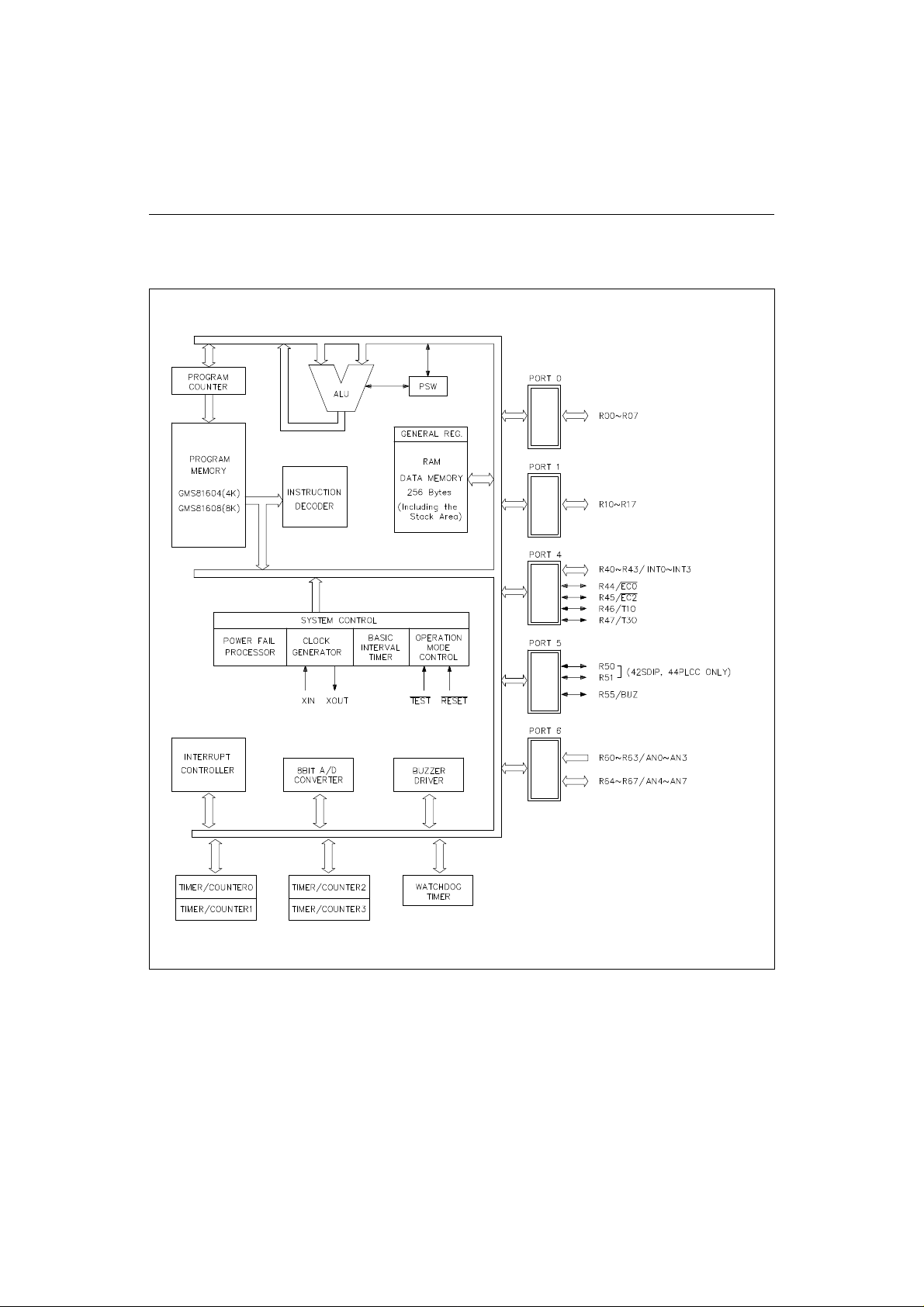
BLOCK DIAGRAM
Figure 1. Block Diagram
3
Page 8
GMS81604/08 LG Semicon
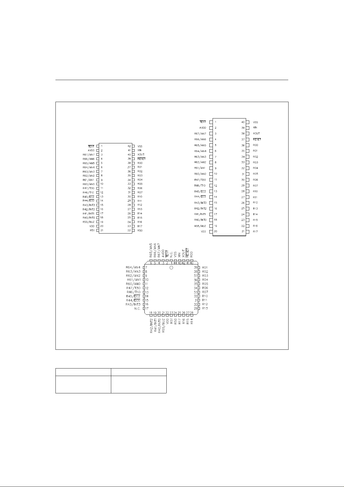
PIN ASSIGNMENT
PACKAGES
Part Package Type
GMS8160X
GMS8160X K
GMS8160X PL
42 SDIP
40DIP
42SDIP
44PLCC
40 PDIP
44 PLCC
Figure 2. Pin Connections
← "X" means 4(4K bytes) or 8(8K bytes).
4
Page 9
LG Semicon GMS81604/08
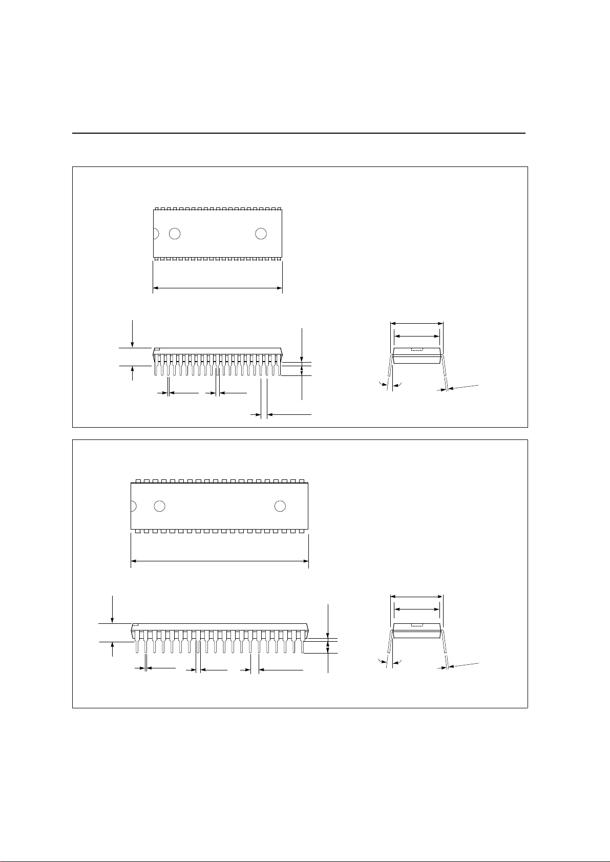
PACKAGE
42SDIP
UNIT: INCH
1.470
1.450
0.600 BSC
0.550
0-15
0.530
2
1
0
.
0
8
0
0
.
°
0
0.190 max.
min. 0.015
0.020
0.016
0.045
0.035
0.140
0.070 BSC
0.120
40DIP
UNIT: INCH
2.075
2.045
0.600 BSC
0.550
0-15
0.530
2
1
0
.
0
8
0
0
.
°
0
5
0.200 max.
0.022
0.015
0.065
0.045
0.100 BSC
min. 0.015
0.140
0.120
Page 10
GMS81604/08 LG Semicon
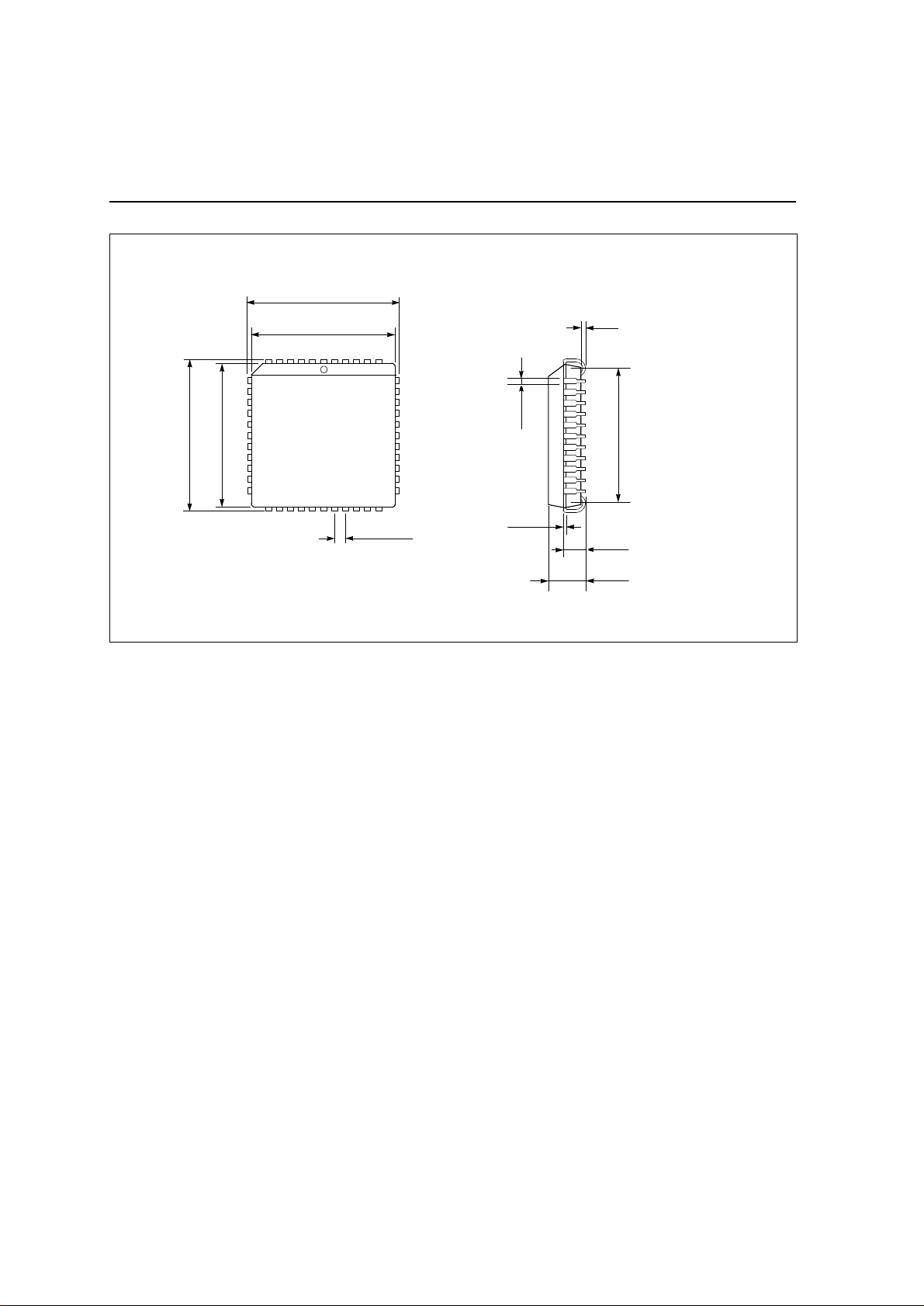
44PLCC
UNIT: INCH
0.695
0.685
min. 0.020
0.630
0.590
0.695
0.685
0.656
0.650
0.656
0.650
0.032
0.026
0.050 BSC
0.012
0.0075
0.120
0.090
0.180
0.165
6
Page 11

LG Semicon GMS81604/08
PIN DESCRIPTIONS
V
: Supply voltage.
DD
V
: Circuit Ground.
SS
TEST: For test purposes only. Connect it to V
DD
.
RESET: Reset the MCU.
X
: Input to the inverting oscillator amplifier and
IN
input to the internal clock operating circuit.
X
: Output from the inverting oscillator amplifier.
OUT
R00~R07: R0 is an 8-bit, CMOS, bidirectional I/O
port. As an output port each pin can sink several LS
TTL inputs. R0 pins that have 1 or 0 written to their
Port Direction Mode Register, can be used as outputs
or inputs.
R10~R17: R1 is an 8-bit, CMOS, bidirectional I/O
port. As an output port each pin can sink several LS
TTL inputs. R1 pins that have 1 or 0 written to their
Port Direction Mode Register, can be used as outputs
or inputs.
R40~R47: R4 is an 8-bit, CMOS, bidirectional I/O
port. As an output port each pin can sink several LS
TTL inputs. R4 pins that have 1 or 0 written to their
Port Direction Mode Register, can be used as outputs
or inputs.
In addition, Port 4 serves the functions of the various
following special features.
Port Pin Alternate Function
R40 INT0 (External Interrupt 0)
R41 INT1 (External Interrupt 1)
R42
R43
R44
R45
R46
R47
INT2 (External Interrupt 2)
INT3 (External Interrupt 3)
EC0 (External Count Input to Timer/
Counter 0)
EC2 (External Count Input to Timer/
Counter 2)
T1O (Timer 1 Clock-Out)
T3O (Timer 3 Clock-Out)
R50, R51, R55: R5 is a 3-bit, CMOS, bidirectional I/O
port. As an output port each pin can sink several LS
TTL inputs. R5 pins that have 1 or 0 written to their
Port Direction Mode Register, can be used as outputs
or inputs. R50 and R51 differs in having internal
pull-ups.
Port R55 serves the functions of special features.
Port Pin Alternate Function
R55 BUZ (Square wave output for Buzzer
driving)
R60~R67: R6 is an 8-bit, CMOS, I/O port. R60~R63
can be used as only input, can not be output, R64~R67
are bidirectional I/O port. As an output port each pin
can sink several LS TTL inputs. R64~R67 pins that
have 1 or 0 written to their Port Direction Mode
Register, can be used as outputs or inputs.
R6 serves the functions of following special features.
Port Pin Alternate Function
R60
R61
R62
R63
R64
R65
R66
R67
AV
: Supply voltage to the ladder resistor of ADC
DD
AN0 (ADC input 0)
AN1 (ADC input 1)
AN2 (ADC input 2)
AN3 (ADC input 3)
AN4 (ADC input 4)
AN5 (ADC input 5)
AN6 (ADC input 6)
AN7 (ADC input 7)
circuit. To enhance the resolution of analog to digital
converter, use independent power source as well as
possible, other than digital power source.
7
Page 12
GMS81604/08 LG Semicon
Port Pin I/O
V
DD
V
SS
AV
DD
Descriptions
Primary Functions Secondary Functions
- Power supply to MCU - - - -
- Ground - - - -
- Power supply for ADC - - - -
Pull-up/
Pull-down
RESET
STOP
Mode
TEST I Test mode - - - RESET I Reset the MCU - Pull-up Low Last state
X
IN
X
OUT
R00~R07 I/O General I/O - - Input
R10~R17 I/O General I/O - - Input
R40/INT0
R41/INT1
R42/INT2
R43/INT3
R44/EC0
R45/EC2
R46/T1O
R47/T3O
1)
R50
1)
R51
R55/BUZ
R60/AN0
R61/AN1
R62/AN2
R63/AN3
R64/AN4
R65/AN5
R66/AN6
R67/AN7
I Oscillation input - - Oscillation Low
O Oscillation output - - Oscillation High
3)
Last state
3)
Last state
I/O
I/O
I/O
I/O
I/O
I/O
I/O
I/O
I/O
I/O
I/O
I
I
I
I
I/O
I/O
I/O
I/O
General I/O
"
"
"
"
"
"
"
General I/O
"
"
General Input
"
"
"
General I/O
"
"
"
External interrupt 0
External interrupt 1
External interrupt 2
External interrupt 3
External count input 0
External count input 2
Timer 1 output
Timer 3 output
-
Buzzer driving output
Analog input 0
Analog input 1
Analog input 2
Analog input 3
Analog input 4
Analog input 5
Analog input 6
Analog input 7
- Input
2)
Pull-up
2)
Pull-up
-
- Input
Input
3)
3)
3)
Last state
Last state
Last state
NOTES:
1. R50 and R51 are not physically served on 40 pin package.
2. When input mode is selected, pull-up is activated. In output mode, pull-up is de-activated.
3. In reset status, status of R50,R51 are weak high (Typ. impedance 50~100kΩ). Other pin impedance is very high(High-Z).
8
Page 13
LG Semicon GMS81604/08
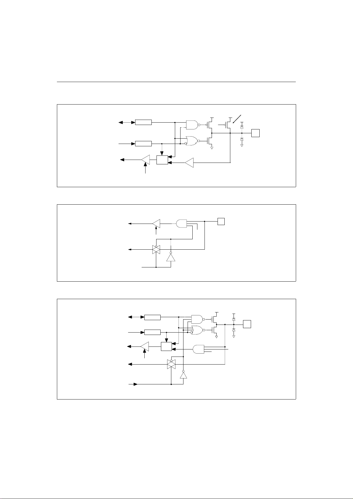
PORT STRUCTURES
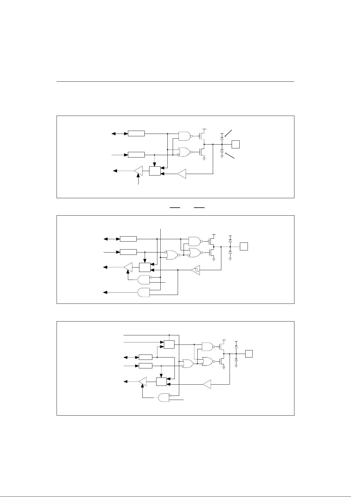
R00~R07, R10~R17
V
DATA BUS
DATA BUS
DATA BUS
DATA REG.
DIRECTION REG.
Rd.
MUX
DD
V
SS
PROTECT DIODE
PROTECT DIODE
R40/INT0, R41/INT1, R42/INT2, R43/INT3, R44/EC0, R45/EC2
PMR4
DATA REG.
DATA BUS
DATA BUS
DIRECTION REG.
DATA BUS
ALTERNATE FUNCTION
EX) INT0
R46/T1O, R47/T3O, R55/BUZ
Selection (PMR4 or PMR5)
ALTERNATE FUNCTION
EX) T1O
DATA BUS
DATA BUS
DATA BUS
MUX
Rd.
MUX
DATA REG.
DIRECTION REG.
MUX
Rd.
9
Page 14
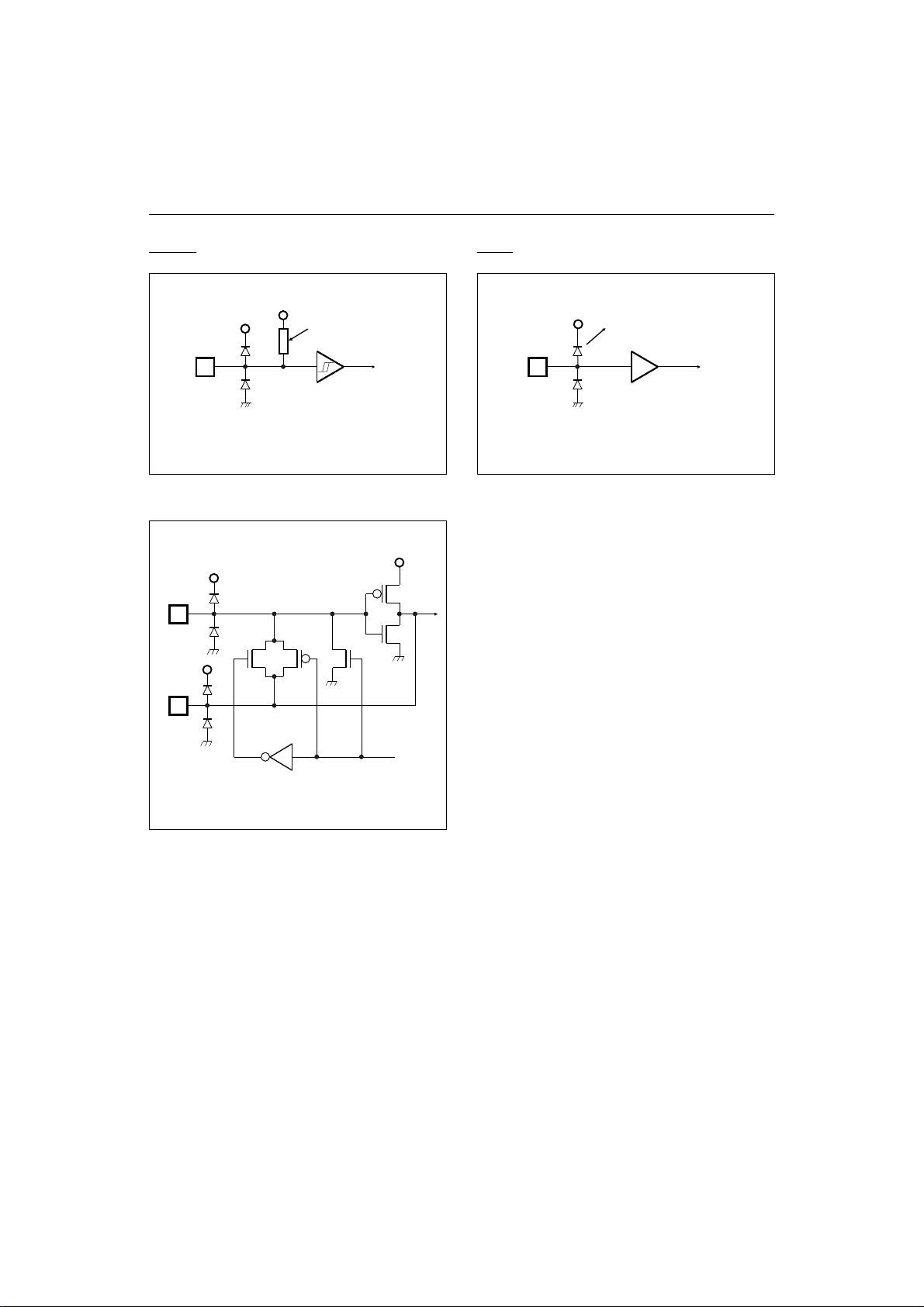
GMS81604/08 LG Semicon
R50, R51
DATA REG.
DATA BUS
DIRECTION REG.
DATA BUS
DATA BUS
Rd.
R60/AN0, R61/AN1, R62/AN2, R63/AN3
DATA BUS
TO A/D Converter
Ch. Select
Rd.
MUX
PULL-UP RESISTOR
INPUT MODE: PULL-UP RESISTOR IS ACTIVATED.
OUTPUT MODE: PULL-UP RESISTOR IS DE-ACTIVATED.
Rd.
R64/AN4, R65/AN5, R66/AN6, R67/AN7
DATA BUS
DATA BUS
DATA BUS
TO A/D Converter
Ch. Select
DATA REG.
DIRECTION REG.
Rd.
10
MUX
0: Output
Rd.
1: Reset, Input, AD ch. select
Page 15
LG Semicon GMS81604/08
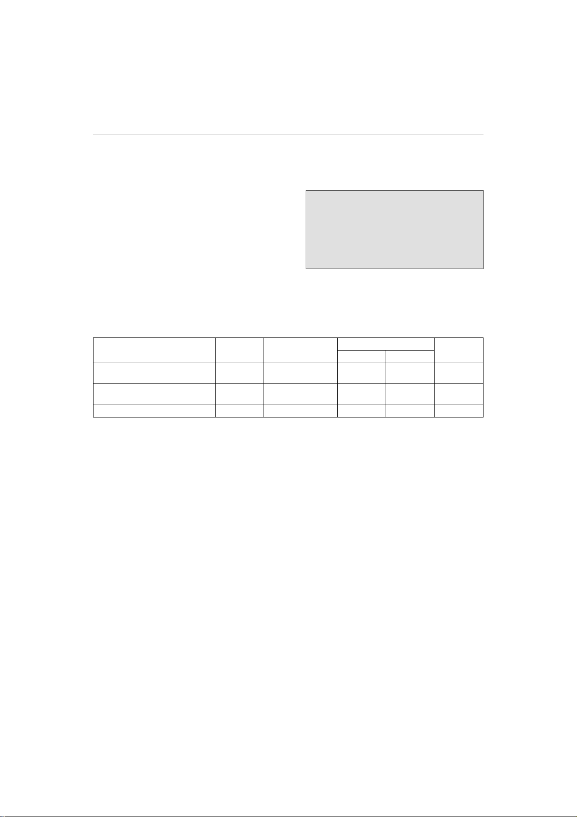
RESET
XIN, X
X
IN
X
OUT
OUT
Pull-up Resister
TEST
OTP: No P-Ch diode
STOP
11
Page 16
GMS81604/08 LG Semicon
ELECTRICAL CHARACTERISTICS
Absolute Maximum Ratings
Supply Voltage . . . . . . . . . . . . . . . -0.3 to +6.0 V
Storage Temperature . . . . . . . . . . . . -40 to +125 °C
Voltage on any pin with
respect to Ground (VSS) . . . . . . -0.3 to VDD+0.3 V
Maximum current out of VSS pin . . . . . . . . . 150 mA
Maximum current into VDD pin . . . . . . . . . 100 mA
Maximum current sunk by (IOL per I/O Pin) . . . . 20 mA
Maximum output current sourced
by (IOH per I/O Pin) . . . . . . . . . . . . . . . 8 mA
Maximum current (Σ IOL) . . . . . . . . . . . . 120 mA
Maximum current (Σ IOH) . . . . . . . . . . . . . 50 mA
Notice:
Stresses above those listed under "Absolute Maximum Ratings" may cause permanent damage to
the device. This is a stress rating only and functional operation of the device at these of any
other conditions above those indicated in the operational sections of this specification is not implied. Exposure to absolute maximum rating
conditions for extended periods may affect device
reliability.
Recommended Operating Conditions
Parameter Symbol Condition
Supply Voltage V
Operating Frequency f
Operating Temperature T
DD
XIN
OPR
f
= 8 MHz
XIN
f
= 4 MHz
XIN
VDD = 4.5~5.5V
VDD = 2.4~5.5V
Specifications
Min. Max.
4.5
2.4
1
1
5.5
5.5
8
4.2
-20 85
Unit
V
MHz
°C
12
Page 17
LG Semicon GMS81604/08
DC Characteristics ( 5V )
(VDD = 5.0V± 10%, VSS = 0V, TA = -20 ~ 85 °C, f
Parameter Pin Symbol Test Condition
XIN, RESET,
Input High Voltage
R40~R45
R0,R1,R46,R47
R5,R6
X
RESET,
IN,
Input Low Voltage
R40~R45
R0,R1,R46,R47
R5,R6
Output High Voltage R0,R1,R4,R5,R6 V
Output Low Voltage R0,R1,R4,R5,R6 V
Power Fail Detect
Voltage
Input Leakage
Current
Input Pull-up Current
Power Current
V
DD
RESET, R0, R1,
R4, R5, R6
RESET I
R50, R51 I
Operating mode I
STOP mode I
Hysteresis
* : Data in "Typ" column is at 5 V, 25°C unless otherwise stated. These parameters are for design guidance only and are not tested.
RESET,
R40~R45
= 8 MHz)
XIN
V
V
V
V
V
PFD
I
I
P1
P2
DD
STOP
VT+
~VT-
Specifications
Min. Typ.* Max.
IH1
IH2
IL1
IL2
OH
OL
- 0.8V
- 0.7V
- 0 - 0.2V
- 0 - 0.3V
VDD = 5V
IOH = -2mA
VDD = 5V
IOL = 10mA
VDD -1.0 VDD -0.4 - V
- 0.6 1.0 V
DD
DD
- V
- V
VDD=3~4V 3.0 - 4.0 V
VI = V
IH
IL
DD
VI = 0V -5.0 - 5.0 uA
-5.0 - 5.0 uA
VDD = 5V -180 -120 -30 uA
VDD = 5V -90 -60 -15 uA
f
XIN
f
XIN
=4MHz
=8MHz
4.5
8
VDD = 5V - 2 20 uA
VDD = 5V 0.5 0.8 - V
15
DD
DD
8
DD
DD
Unit
V
V
V
V
mA
A/D Converter Characteristics ( 5V )
(VDD = 5.0V± 10%, V
Parameter Symbol
Analog Input Range V
Non-linearity Error N
Differential Non-linearity Error N
Zero Offset Error N
Full Scale Error N
Accuracy A
AVDD Input Current I
Conversion Time T
Analog power supply Input
Range
* : Data in "Typ" column is at 5 V, 25°C unless otherwise stated. These parameters are for design guidance only and are not tested.
= 5.0V, VSS = 0V, TA = 25 °C)
AIN
AVDD
V
AIN
LE
DIF
OFF
FS
CC
CONV
AVDD
Specifications
Min. Typ.* Max.
V
SS
- 0.7
- 0.1
- 1.5
- 1.0
- 2.0
- V
AVDD
± 1.5
± 0.5
± 2.5
± 1.5
± 3.0
- 0.5 1.0 mA
- - 40 uS
4.5 5.0 5.5
Unit
V
LSB
LSB
LSB
LSB
LSB
V
13
Page 18
GMS81604/08 LG Semicon
DC Characteristics ( 3V )
(VDD = 3.0V± 10%, VSS = 0V, TA = -20 ~ 85 °C, f
Parameter Pin Symbol Test Condition
XIN, RESET,
Input High Voltage
R40~R45
R0,R1,R46,R47
R5,R6
XIN, RESET,
Input Low Voltage
R40~R45
R0,R1,R46,R47
R5,R6
Output High Voltage R0,R1,R4,R5,R6 V
Output Low Voltage R0,R1,R4,R5,R6 V
Power Fail Detect
Voltage**
Input Leakage
Current
Input Pull-up
Current
Power Current
Hysteresis
* : Data in "Typ" column is at 3 V, 25°C unless otherwise stated. These parameters are for design guidance only and are not tested.
**: Power Fail Detection function is not available on 3V operation.
- - - - - - V
RESET, R0, R1,
R4, R5, R6
RESET I
R50, R51 I
Operating mode I
STOP mode I
RESET,
R40~R45
= 4 MHz)
XIN
V
V
V
V
I
I
P1
P2
DD
STOP
VT+
~VT-
Specifications
Min. Typ.* Max.
IH1
IH2
IL1
IL2
OH
OL
IH
IL
- 0.8V
- 0.7V
- 0 - 0.2V
- 0 - 0.3V
VDD = 3V
IOH = -1mA
VDD = 3V
IOL = 5mA
VI = V
DD
VDD -0.5 VDD -0.3 - V
- 0.5 0.7 V
-3.0 - 3.0 uA
VI = 0V -3.0 - 3.0 uA
DD
DD
- V
- V
VDD = 3V -60 -40 -15 uA
VDD = 3V -30 -20 -7.5 uA
f
=4MHz - 2 5 mA
XIN
VDD = 3V - 1 10 uA
VDD = 3V 0.3 0.6 - V
DD
DD
DD
DD
Unit
V
V
V
V
A/D Converter Characteristics ( 3V )
(VDD = 3.0V± 10%, V
Parameter Symbol
Analog Input Range V
Non-linearity Error N
Differential Non-linearity Error N
Zero Offset Error N
Full Scale Error N
Accuracy A
AVDD Input Current I
Conversion Time T
Analog power supply Input
Range
* : Data in "Typ" column is at 3 V, 25°C unless otherwise stated. These parameters are for design guidance only and are not tested.
= 3.0V, VSS = 0V, TA = 25 °C)
AIN
AVDD
V
AIN
LE
DIF
OFF
FS
CC
CONV
AVDD
Specifications
Min. Typ.* Max.
V
SS
- 0.2
- 0.1
- 2.0
- 1.0
- 2.0
- V
AVDD
± 1.0
± 0.5
± 2.5
± 1.5
± 3.0
- 0.3 0.5 mA
- - 40 uS
2.7 3.0 3.3
Unit
V
LSB
LSB
LSB
LSB
LSB
V
14
Page 19
LG Semicon GMS81604/08
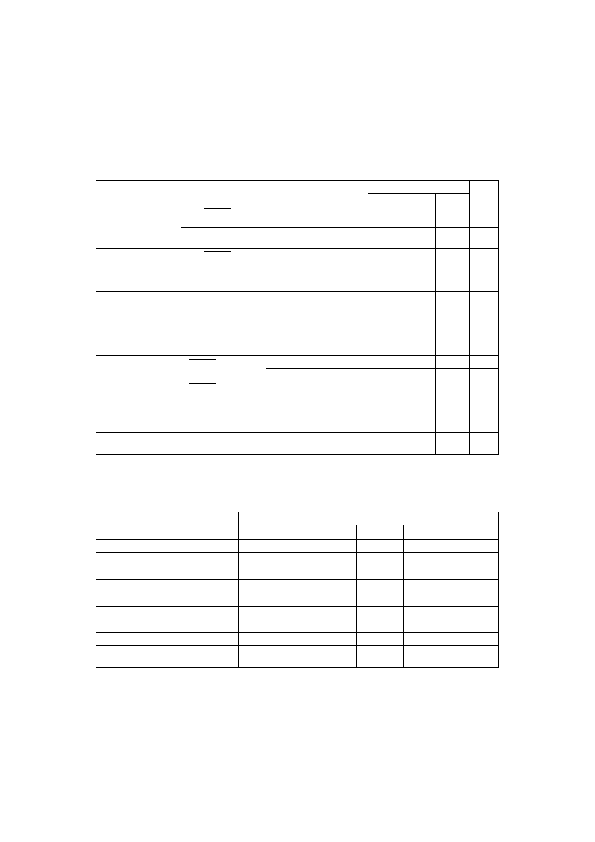
AC Characteristics
(VDD = 2.7~5.5V, VSS = 0V, TA = -20 ~ 85 °C)
Parameter Pin Symbol
Main clock frequency X
Oscillation stabilization Time XIN, X
External Clock Pulse Width X
External Clock Transition Time X
IN
OUT
IN
IN
Interrupt Pulse Width INT0, INT1, INT2, INT3 t
RESET Input Low Width RESET t
Event Counter Input Pulse
Width
EC0, EC2 t
Event Counter Transition Time EC0, EC2 t
*: t
is 2/f
XIN
.
SYS
t
RCP
REC
f
t
t
CPW
RST
ECW
XIN
ST
, t
IW
, t
FCP
FEC
Specifications
Min. Typ. Max.
1 - 8 MHz
20 - - ms
80 - - ns
- - 20 ns
2 - - t
8 - - t
2 - - t
- - 20 ns
Unit
SYS
SYS
SYS
*
*
*
Timing Chart
t
1 / f
XIN
X
IN
CPWtCPW
0.9V
0.1V
DD
DD
INT0, INT1
INT2, INT3
RESET
EC0, EC2
0.8V
t
RCPtFCP
t
IW
DD
0.8V
t
REC
0.2V
DD
t
RST
t
ECW
DD
t
0.2V
FEC
DD
0.2V
t
ECW
t
IW
DD
15
Page 20
GMS81604/08 LG Semicon
TYPICAL CHARACTERISTICS
These parameters are for design guidance only and are not tested.
VDD=5V
I
DD
(mA)
I
OL
(mA)
IDD - V
DD
TA=25°C
8
6
4
2
IOL - V
VDD=5.0V
24
18
12
6
0
f
XIN
f
= 4MHz
XIN
2 3 4 506 (V)
OL
TA=25°C
1 2 3 4
= 8MHz
I
STOP
I
STOP
(uA)
TA=25°C
8
6
4
2
V
DD
I
(mA)
V
OL
(V)
2 3 4 506 (V)
IOH - V
OH
24
18
12
6
0
OH
VDD=5.0V
TA=25°C
1 2 3 4
VDD-V
(V)
V
DD
OH
16
Operating area
f
XIN
(MHz)
TA = -20~80°C
8
6
4
2
0
1
2 3 4 5
V
DD
(V)
Page 21
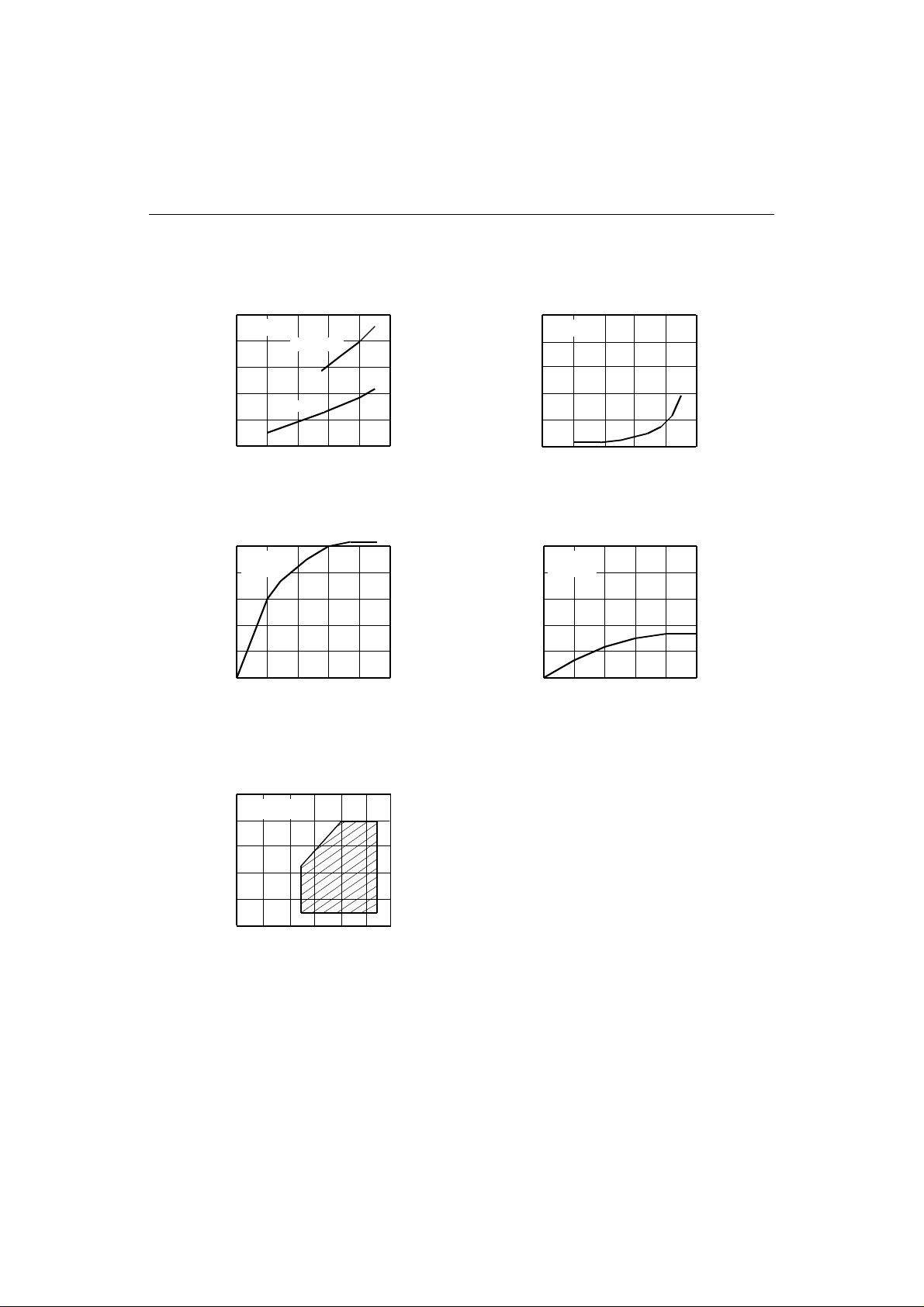
LG Semicon GMS81604/08
VDD=3.0V
I
OL
(mA)
20
IOL - V
VDD=3.0V
TA=25°C
OL
I
OH
(mA)
-8
IOH - V
VDD=3.0V
TA=25°C
OH
15
10
5
0
0.5 1.0 1.5 2.0
-6
-4
-2
VDD-V
V
OL
(V)
0
0.5 1.0 1.5 2.0
OH
(V)
17
Page 22
GMS81604/08 LG Semicon
MEMORY ORGANIZATION
The GMS81604 has separate address spaces for Program and Data Memory. Program memory can only be
read, not written to. It can be up to 4K (8K for
GMS81608) bytes of Program Memory. Data memory can be read and written to up to 256 bytes including
the stack area.
Registers
This device has six registers that are the Program
Counter (PC), a Accumulator (A), two Index registers
(X,Y), the Stack Pointer (SP) and the Program Status
Word (PSW). The Program Counter consists of 16-bit
register.
A
X
Y
SP
PCH PCL
PSW
ACCUMULATOR
X REGISTER
Y REGISTER
STACK POINTER
PROGRAM COUNTER
PROGRAM STATUS
WORD
Figure 3. Configuration of Registers
Accumulator: The accumulator is the 8-bit general
purpose register, used for data operation such as transfer, temporary saving and conditional judgment, etc.
The accumulator can be used as a 16-bit register with
Y register as shown below.
Y
Y A
A
TWO 8-BIT REGISTERS ONE "YA" 16-BIT REGISTER
Figure 4. Configuration of YA 16-bit register
X register, Y register: In the addressing modes which
use these index registers, the register contents are
added to the specified address and this becomes the
actual address. These modes are extremely effective
for referencing subroutine tables and memory tables.
The index registers also have increment, decrement,
compare and data transfer functions and they can be
used as simple accumulators.
Stack Pointer: The stack pointer is an 8-bit register
used for occurrence interrupts and calling out subroutines. The stack can be located at any position within
100H to 13FH of the internal data memory. Data store
and restore sequence to(from) stack area is shown in
Figure 0.
Caution:
The stack pointer must be initialized by software
because its value is undefined after reset.
Ex) LDX #03FH
TXSP ; SP ← 3F
Stack Address (100H~13FH)
15 8 7 0
1 SP
Hardware fixed.
H
Figure 5. Stack Pointer
Program Counter: The program counter is a 16-bit
wide which consists of two 8-bit registers, PCH, PCL.
This counter indicates the address of the next instruction to be executed. In reset state, the program counter
has reset routine address (PCH: FFH, PCL: FEH). .
Program Status Word : The Program Status Word
(PSW) contains several status bits that reflect the current state of the CPU. The PSW shown in Figure 6. It
contains the Negative flag, the Overflow flag, the
Direct page flag, the Break flag, the Half Carry (for
BCD operations), the Interrupt enable flag, the Zero
flag and the Carry bit.
[Carry flag C]
This flag stores any carry or borrow from the ALU of
CPU after an arithmetic operation and is also changed
by the Shift instruction or rotate instruction.
[Zero flag Z]
This flag is set when the result of an arithmetic operation or data transfer is "0" and is cleared by any other
result.
[Interrupt disable flag I] This flag enables/disables all
interrupts except interrupt caused by Reset or software
18
Page 23
LG Semicon GMS81604/08
MSB LSB
PSW
NEGATIVE FLAG
OVERFLOW FLAG
N
V G B H I Z C
RESET VALUE: 00H
CARRY FLAG RECEIVES
CARRY OUT
ZERO FLAG
G FLAG TO SELECT DIRECT PAGE
BRK FLAG
Figure 6. PSW (Program Status Word) Register
BRK instruction. All interrupts are disabled when
cleared to "0". This flag immediately becomes "0"
when an interrupt is served. It is set by the EI instruction, cleared by the DI instruction.
[Half carry flag H]
After operation, set when there is a carry from bit 3 of
ALU or there is not a borrow from bit 4 of ALU. This
bit can not be set or cleared except CLRV instruction,
clearing with Overflow flag (V).
[Break flag B]
This flag set by software BRK instruction to distinguish BRK from TCALL instruction which as the
same vector address.
[Direct page flag G]
This flag assign direct page for direct addressing mode.
In the direct addressing mode, addressing area is
INTERRUPT ENABLE
FLAG
HALF CARRY FLAG RECEIVES
CARRY OUT FROM BIT 1 OF
ADDITION OPERANDS
within zero page 00H to FFH when this flag is "0". If it
is set to "1", addressing area is 100H to 1FFH.
It is set by SETG instruction, and cleared by CLRG.
[Overflow flag V]
This flag is set to "1" when an overflow occurs in the
result of an arithmetic operation involving signs. An
overflow occurs when the result of an addition or
subtraction exceeds +127(7FH) or -128(80H).
The CLRV instruction clears the overflow flag. There
is no set instruction. When the BIT instruction is
executed, for other than the above, bit 6 of memory is
copy to this flag.
[Negative flag N]
This flag is set to match the sign bit (bit 7) status of the
result of a data or arithmetic operation. When the BIT
instruction is executed, bit 7 of memory is copy to this
flag.
1) INTERRUPT
M(SP) ← (PCH)
SP ← SP - 1
M(SP) ← (PCL)
SP ← SP - 1
M(SP) ← (PSW)
SP ← SP - 1 (PCH) ← M(SP)
2) RETI
SP ← SP + 1
(PSW) ← M(SP)
SP ← SP + 1
(PCL) ← M(SP)
SP ← SP + 1
3) CALL
M(SP) ← (PCH)
SP ← SP - 1
M(SP) ← (PCL)
SP ← SP - 1
Figure 7. Stack Operation
4) RET
SP ← SP + 1
(PCL) ← M(SP)
SP ← SP + 1
(PCH) ← M(SP)
5) PUSH A (X,Y,PSW)
M(SP) ← ACC.
SP ← SP - 1
6) POP A (X,Y,PSW)
SP ← SP + 1
M(SP) ← (PCH)
19
Page 24
GMS81604/08 LG Semicon
Program Memory
A 16-bit program counter is capable of addressing up
to 64K bytes, but this devices have 4K bytes (8K for
GMS81608) program memory space only the physically implemented. Accessing a location above FFFF
will cause a wrap-around to 0000H.
Figure 8, shows a map of the upper part of the Program
Memory. After reset, the CPU begins execution from
reset vector which is stored in address FFFEH, FFFFH.
As shown in Figure 8, each area is assigned a fixed
location in Program Memory. Program Memory area
contains the user program, Page Call (PCALL) area
contains subroutine program, to reduce program byte
length because of using by 2 bytes PCALL instead of
3 bytes CALL instruction. If it is frequently called,
more useful to save program byte length.
E000H
F000H
PROGRAM
MEMORY
FEFFH
FF00H
FFBFH
FFC0H
FFDFH
FFE0H
FFFFH
PCALL
AREA
TCALL
AREA
INTERRUPT
VECTOR
AREA
GMS81608
GMS81604
Figure 8. Program Memory
Table Call (TCALL) causes the CPU to jump to each
TCALL address, where it commences execution of the
service routine. The Table Call service locations are
spaced at 2-byte interval : FFC0H for TCALL15,
FFC2H for TCALL14, etc.
Address TCALL Name
FFC0H
FFC2H
FFC4H
H
FFC6H
FFC8H
FFCAH
FFCCH
FFCEH
FFD0H
FFD2H
FFD4H
FFD6H
FFD8H
FFDAH
FFDCH
FFDEH
1) The BRK software interrupt is using same address with
TCALL0.
TCALL15
TCALL14
TCALL13
TCALL12
TCALL11
TCALL10
TCALL9
TCALL8
TCALL7
TCALL6
TCALL5
TCALL4
TCALL3
TCALL2
TCALL1
TCALL0/ BRK
1)
The interrupt causes the CPU to jump to specific
location, where it commences execution of the service
routine. The External interrupt 0, for example, is assigned to location FFFAH. The interrupt service locations are spaced at 2-byte interval : FFF8H for External
Interrupt 1, FFFAH for External Interrupt 0, etc.
Any area from FF00H to FFFFH, if it not going to be
used, its service location is available as general purpose Program Memory.
Address Vector Name
FFE0H
FFE2H
FFE4H
FFE6H
FFE8H
FFEAH
FFECH
FFEEH
FFF0H
FFF2H
FFF4H
FFF6H
FFF8H
FFFAH
FFFCH
FFFEH
-
-
Basic Interval Timer
Watch Dog Timer
Analog to Digital Converter
Timer/ Counter 3
Timer/ Counter 2
Timer/ Counter 1
Timer/ Counter 0
External Interrupt 3
External Interrupt 2
External Interrupt 1
External Interrupt 0
RESET
20
Page 25

LG Semicon GMS81604/08
Data Memory
Figure 9 shows the internal Data Memory space available. Data Memory are divided into three groups, a
user RAM, control registers and Stack.
00
H
DATA
MEMORY
(RAM)
BF
C0
100
13F
FF
H
H
CONTROL
REGISTERS
H
H
STACK
H
AREA
256 BYTES
Figure 9. Data Memory
Internal Data Memory addresses are always one byte
wide, which implies an address space of 256 bytes
including the stack area. To access above FFH, G-flag
should be set to "1" before, because after MCU reset,
G-flag is "0".
The stack pointer should be initialized within 00H to
3FH by software because of implemented area of
internal data memory.
The control registers are used by the CPU and Peripheral functions for controlling the desired operation of
the device.
Therefore these registers contain control and status
bits for the interrupt system, the timer/ counters, analog
to digital converters, I/O ports. The control registers
are in address C0H to FFH.
Note that unoccupied addresses may not be implemented on the chip. Read accesses to these addresses
will in general return random data, and write accesses
will have an indeterminate effect.
More detail informations of each register are explained
in each peripheral sections.
Caution:
Write only registers can not be accessed by bit
manipulation instruction.
Address Symbol R/W
C0
C1
C2
C3
C8
C9
CA
CB
CC
CD
D0
D1
D3
D3
E0
E2
E3
E4
E5
E6
E7
E8
E9
EC
ED
F4
F5
F6
F7
F8
Legend - = Unimplemented locations.
X= Undefined value.
NOTES:
1) The all write only registers can not be accessed by bit
manipulation instruction.
2) The register BITR and CKCTLR are located at same address.
Address D3H is read as BITR, as written to CKCTLR.
3) Several names are given at same address. Refer to below
table.
Address
E4H
E5H
E6H
E7H
4) Only bit 0 of ADCM can be read.
R0
H
R0DD
H
R1
H
R1DD
H
R4
H
R4DD
H
R5
H
R5DD
H
R6
H
R6DD
H
PMR4
H
PMR5
H
2)
BITR
H
2)
CKCTLR
H
WDTR
H
TM0
H
TM2
H
H
H
H
H
H
H
H
H
H
H
H
H
H
Note 3
+
Note 3
+
Note 3
+
Note 3
+
ADCM
ADR
BUR
PFDR
IENL
IRQL
IENH
IRQH
IEDS
Timer mode Capture Mode
T0
T1
T2
T3
When read
R/W
1)
W
R/W
W
R/W
W
R/W
W
R/W
W
W
W
R
W
W
R/W
R/W
R/W
R/W
R/W
R/W
R/W
R
W
R/W
R/W
R/W
R/W
R/W
W
CDR0
CDR1
CDR2
CDR3
1)
1)
1)
1)
1)
1)
1)
1)
1)
1)
Reset Value
4)
Power-on
X
00000000
X
00000000
X
00000000
X
--0---00
X
00000000
00000000
--0-----
00000000
--010111
-0111111
00000000
00000000
X
X
X
X
--000001
X
X
-----100
000----000----00000000
00000000
00000000
When write
TDR0
TDR1
TDR2
TDR3
21
Page 26

GMS81604/08 LG Semicon
Control Registers for the GMS81604/08
Address Name Bit 7 Bit 6 Bit 5 Bit 4 Bit 3 Bit 2 Bit 1 Bit 0
C0
C1
C2
C3
C8
C9
CA
CB
CC
CD
D0
D1
D3
D3
E0
E2
E3
E4
E5
E6
E7
E8
E9
EC
ED
F4
F5
F6
F7
F8
Legend - = Unimplemented locations.
R0 R0 port data register
H
R0DD R0 port direction register
H
R1 R1 port data register
H
R1DD R1 port direction register
H
R4 R4 port data register
H
R4DD R4 port direction register
H
R5 R5 port data register
H
R5DD R5 port direction register
H
R6 R6 port data register
H
R6DD R6 port direction register
H
PMR4 T3S T1S EC2S EC0S INT3S INT2S INT1S INT0S
H
PMR5 - - BUZS - - - - -
H
1)
BITR Basic Interval Timer data register
H
1)
CKCTLR - - WDTON ENPCK BTCL BTS2 BTS1 BTS0
H
WDTR - WDTCL 6-bit Watch Dog Counter register
H
TM0 CAP0 T1ST T1SL1 T1SL0 T0ST T0CN T0SL1 T0SL0
H
TM2 CAP2 T3ST T3SL1 T3SL0 T2ST T2CN T2SL1 T2SL0
H
T0/ TDR0/ CDR0 Timer 0 register/ Timer data register 0/ Capture data register 0
H
T1/ TDR1/ CDR1 Timer 1 register/ Timer data register 1/ Capture data register 1
H
T2/ TDR2/ CDR2 Timer 2 register/ Timer data register 2/ Capture data register 2
H
T3/ TDR3/ CDR3 Timer 3 register/ Timer data register 3/ Capture data register 3
H
ADCM - - ADEN ADS2 ADS1 ADS0 ADST ADSF
H
ADR ADC result data register
H
BUR BUCK1 BUCK0 BU5 BU4 BU3 BU2 BU1 BU0
H
2)
PFDR - - - - - PFD PFR PFS
H
IENL AE WDTE BITE - - - - -
H
IRQL AIF WDTIF BITIF - - - - -
H
IENH INT0E INT1E INT2E INT3E T0E T1E T2E T3E
H
IRQH INT0IF INT1IF INT2IF INT3IF T0IF T1IF T2IF T3IF
H
IEDS IED3H IED3L IED2H IED2L IED1H IED1L IED0H IED0L
H
NOTES:
1) The register BITR and CKCTLR are located at same address. Address D3H is read as BITR, written to CKCTLR.
2) The register PFDR only be implemented on device, not on In-circuit Emulator.
22
Page 27

LG Semicon GMS81604/08
I/O PORTS
The GMS81604/08 have five ports, R0, R1, R4, R5,
R6. These ports pins may be multiplexed with an
alternate function for the peripheral features on the
device. In general, when a initial reset state, all ports
are used as a general purpose input port.
All pins have data direction registers which can configure these pins as output or input.
A "1" in the port direction register configures the
corresponding port pin as output. Conversely, write
"0" to the corresponding bit to specify as an input pin.
For example, to use the even numbered bit of R1 as
output ports and the odd numbered bits as input ports,
write "55H" to address C1H (R0 direction register)
during initial setting as shown in Figure 10.
WRITE "55H" TO PORT R0 DIRECTION REGISTER
C0H
C1H
C2H
C3H
R0 DATA
R0 DIRECTION
R1 DATA
R1 DIRECTION
0 1 0 1 0 1 0 1
7 6 5 4 3 2 1 0 BIT
I I O I O I OO
7 6 5 4 3 2 1 0 PORT
I: INPUT PORT
O: OUTPUT PORT
Figure 10. Example port I/O assignment
Reading data register reads the status of the pins
whereas writing to it will write to the port latch.
R0 and R0DD registers: R0 is a 8-bit bidirectional
I/O port (address C0H). Each pin is individually configurable as input and output through the R0DD register (address C1H).
Port 0 Data Register
R07 R06 R05 R04 R03 R02 R01 R00
R0
Port 0 Direction Register
R07 R06 R05 R04 R03 R02 R01 R00
R0DD
ADDRESS: C0
RESET VALUE: Undefined
Input/ Output data
ADDRESS: C1
RESET VALUE: 00000000
Direction select
0: Input
1: Output
H
H
R1 and R1DD registers: R1 is an 8-bit bidirectional
I/O port (address C2H). Each pin is individually configurable as input and output through the R1DD register (address C3H).
Port 1 Data Register
R17 R16 R15 R14 R13 R12 R11 R10
R1
Port 1 Direction Register
R17 R16 R15 R14 R13 R12 R11 R10
R1DD
ADDRESS: C2
RESET VALUE: Undefined
Input/ Output data
ADDRESS: C3
RESET VALUE: 00000000
Direction select
0: Input
1: Output
H
H
R4 and R4DD registers: R4 is an 8-bit bidirectional
I/O port (address C8H). Each pin is individually configurable as input and output through the R4DD register (address C9H).
In addition, Port R4 is multiplexed with various special
features. The control register PMR4 (address D0H)
controls to select alternate function. After reset, this
value is "0", port may be used as general I/O ports. To
select alternate function such as External interrupt or
External counter or Timer clock out, write "1" to the
corresponding bit of PMR4.
Port Pin Alternate Function
R40
R41
R42
R43
R44
INT0 (External Interrupt 0)
INT1 (External Interrupt 1)
INT2 (External Interrupt 2)
INT3 (External Interrupt 3)
EC0 (External Count Input to Timer/
Counter 0)
R45
EC2 (External Count Input to Timer/
Counter 2)
R46
R47
T1O (Timer 1 Clock-Out)
T3O (Timer 3 Clock-Out)
Regardless of the direction register R4DD, PMR4 is
selected to use as alternate functions, port pin can be
used as a corresponding alternate features.
23
Page 28

GMS81604/08 LG Semicon
R5 and R5DD registers: R5 is a 3-bit bidirectional
Port 4 Data Register
R47 R46 R45 R44 R43 R42 R41 R40
R4
ADDRESS: C8
RESET VALUE: Undefined
H
I/O port (address CAH). R50, R51 and R55 only are
physically implemented on this device.
R50, R51 have internal pullups which is activated on
input but deactivated on output. As input, these pins
Input/ Output data
that are externally pull low will source current (IP2 on
the DC characteristics) because of the internal pullups.
Port 4 Direction Register
R47 R46 R45 R44 R43 R42 R41 R40
R4DD
Port 4 Mode Register
T3S T1S EC2S EC0S INT3S INT2S INT1S INT0S
PMR4
0: R46
1: T1O
0: R47
1: T3O
Edge Selection Register
MSB LSB
IEDS
INT3 INT2 INT1 INT0
External Interrupt Edge select
00: Reserved
01: Falling (1-to-0 transition)
10: Rising (0-to-1 transition)
11: Both (Rising & Falling)
ADDRESS: C9
RESET VALUE: 00000000
Direction select
0: Input
1: Output
ADDRESS: D0
RESET VALUE: 00000000
0: R44
1: EC0
0: R45
1: EC2
ADDRESS: F8
RESET VALUE: 00000000
0: R43
1: INT3
H
H
0: R42
1: INT2
H
0: R41
1: INT1
0: R40
1: INT0
Caution:
Pins R50, R51 are present on 42SDIP, 44PLCC
package only, but not on 40DIP . Refer to Pin assignment.
Each pin is individually configurable as input and
output through the R5DD register (address CBH).
Port Pin Alternate Function
R55 BUZ (Square-wave output for
Buzzer driving)
The control register PMR5 (address D1H) controls the
selection alternate function. After reset, this value is
"0", port may be used as general I/O ports. To use
buzzer function, write "1" to the PMR5.
Port 5 Data Register
- - R55 - - - R51 R50
R5
Port 5 Direction Register
R5DD
- - R55 - - - R51 R50
Port 5 Mode Register
PMR5
- - BUZS - - - - -
ADDRESS: CA
RESET VALUE: Undefined
Input/ Output data
ADDRESS: CB
RESET VALUE: --0---00
Direction select
0: Input
1: Output
ADDRESS: D1
RESET VALUE: --0-----
H
H
H
24
0: R55
1: BUZ (Buzzer Port)
Page 29

LG Semicon GMS81604/08
R6 and R6DD registers: R6 is an 8-bit port (address
CCH). Pins R64~R67 are indiv idual ly confi gurabl e as
input and output th rough the R6DD registe r (address
CDH), but pins R60~R63 are input only.
Port Pin Alternate Function
R60
R61
R62
R63
R64
R65
R66
R67
AN0 (ADC input 0)
AN1 (ADC input 1)
AN2 (ADC input 2)
AN3 (ADC input 3)
AN4 (ADC input 4)
AN5 (ADC input 5)
AN6 (ADC input 6)
AN7 (ADC input 7)
R6DD (address CDH) controls the direction of the R6
pins, even when they are being used as analog inputs.
The user must make sure to keep the pins configured
as inputs when using them as analog inputs.
On the initial RESET, R60 can not be used digital
input port, because this port is selected as an analog input port by ADCM register. To use this port as
a digital I/O port, change the value of lower 4 bits of
ADCM (address 0E8
On the other hand, R6 port, all eight pins can not be
used as digital I/O port simultaneousely. At least
one pin is used as an analog input.
).
H
Port 6 Data Register
R67 R66 R65 R64 R63 R62 R61 R60
R6
Port 6 Direction Register
R67 R66 R65 R64 R63 R62 R61 R60
R6DD
ADDRESS: CC
RESET VALUE: Undefined
Input/ Output data
ADDRESS: CD
RESET VALUE: 0000----
H
H
Fixed as Input.
Can not write.
Direction select
0: Input
1: Output
25
Page 30

GMS81604/08 LG Semicon
BASIC INTERVAL TIMER
The GMS81604 has one 8-bit Basic Interval Timer that
is free-run, can not stop. Block diagram is shown in
Figure 11.
The 8-bit Basic interval timer register (BITR) is incremented every internal count pulse which is divided by
prescaler. Since prescaler has divided ratio by 16 to
2048, the count rate is 1/16 to 1/2048 of the oscillator
frequency. As the count overflows from FFH to 00H,
this overflow causes to generate the Basic interval
timer interrupt. The BITR is interrupt request flag of
BTS[2:0]
3
8
MUX
XIN PIN
÷16
÷32
÷64
÷128
÷256
÷512
÷1024
÷2048
PRESCALER
Figure 11. Block Diagram of The Basic Interval Timer
CKCTLR
WDTON- ENPCK BTCL BTS1BTS2 BTS0-
Basic interval timer.
Caution:
All control bits of Basic interval timer are in
CKCTLR register which is located at same address of BITR (address D3H). Address D3H is
read as BITR, written to CKCTLR.
When write "1" to bit BTCL of CKCTLR, data register
is cleared to "0" and restart to count-up. It becomes "0"
after one machine cycle by hardware.
BTCL
CLEAR
BITR (8 BITS)
BITIF
BASIC INTERVAL TIMER
INTERRUPT
ADDRESS: D3
RESET VALUE: --010111
H
26
Symbol Position Name and Significance
WDTON CKCTLR.5
ENPCK CKCTLR.4 Enable Peripheral clock.
BTCL CKCTLR.3
BASIC INTERVAL TIMER CLOCK SELECTION
BTS2 BTS1 BTS0 Prescale value
0
0
0
0
0
1
0
1
1
0
1
0
1
1
1
1
WDTON=1, enables Watch Dog Timer operation,
WDTON=0, operates as a 6-bit timer
BTCL is set to "1", BITR is cleared. BTCL becomes "0" automatically
after one machine cycle, and starts counting.
0
1
0
1
0
1
0
1
16
32
64
128
256
512
1024
2048
Figure 12. CKCTLR: Control Clock Register
Page 31

LG Semicon GMS81604/08
TIMER/COUNTER
The GMS81604 has four Timer/Counter registers.
Each module can generate an interrupt to indicate that
an event has occurred (i.e. timer match).
Timer 0 and Timer 1 are can be used either the two
8-bit Timer/Counter or one 16-bit Timer/Counter to
combine them. Also Timer 2 and Timer 3 are same.
In the "timer" function, the register is incremented
every internal clock input. Thus, one can think of it as
counting internal clock input. Since a least clock consists of 4 and most clock consists of 64 oscillator
periods, the count rate is 1/4 to 1/64 of the oscillator
frequency.
In the "counter" function, the register is incremented
in response to a 1-to-0 (falling edge) transition at its
corresponding external input pin, EC0 or EC2.
In addition the "capture" function, the register is incremented in response external or internal clock sources
same with timer or counter function. When external
clock edge input, the count register is captured into
Timer data register correspondingly.
It has four operating modes: "8-bit timer/counter",
"16-bit timer/counter", "8-bit capture", "16-bit capture" which are selected by bit in Timer mode register
TM0 and TM2 as shown in right Table.
In operation of Timer 2, Timer 3, their operations are
same with Timer 0, Timer 1, respectively.
TM0 FOR TIMER 0, TIMER 1
CAP0 T1SL1 T1SL0 Timer 0 Timer 1
0 0 0 16-bit Timer/Counter
1 0 0 16-bit Capture
0 X X 8-bit Timer 8-bit Timer
1 X X 8-bit Capture 8-bit Timer
TM2 FOR TIMER 2, TIMER 3
CAP2 T3SL1 T3SL0 Timer 2 Timer 3
0 0 0 16-bit Timer/Counter
1 0 0 16-bit Capture
0 X X 8-bit Timer 8-bit Timer
1 X X 8-bit Capture 8-bit Timer
LSBMSB
TM0
TM2 is in Figure 14.
Capture mode selection flag, When set, timer
CAP0
operate as one 16-bit capture timer combine
two 8-bit timers.
When set, Timer 1 count register is cleared
T1ST Start/Stop control for Timer 0. A logic 1
and start again.
When cleared, stop the counting.
TIMER 1 TIMER 0
T1SL1 T1SL0
0
0
1
1
NOTE:
If this mode selected, the Timer 0 are used as a 16-bit timer mode. The Timer 1 is engaged to the Timer 0.
The source clock is selected by bits T0SL1 and T0SL0.
INPUT CLOCK
0
16-BIT TIMER MODE (NOTE 1)
1
8-BIT TIMER, ÷ 4 ← PRESCALER
0
8-BIT TIMER, ÷ 16
1
8-BIT TIMER, ÷ 64
T1SL1T1ST T1SL0 T0ST T0SL1T0CN T0SL0CAP0
TIMER 1 TIMER 0
When set, The Timer 0 Count Register is
T0ST
cleared and start again.
When cleared, stop the counting.
T0CN
starts the timer.
T0SL1 T0SL0
0
0
0
1
1
0
1
1
INPUT CLOCK
Timer or Counter select
÷ 4 ← PRESCALER
÷ 16
÷ 64
ADDRESS: E2
RESET VALUE: 00H
Figure 13. TM0: Timer 0, Timer 1 Mode Register
H
27
Page 32

GMS81604/08 LG Semicon
MSB
TM2
Capture mode selection flag, When set, timer
CAP2
operate as one 16-bit timer combine two 8-bit
timers. See Figure 21 and Figure 22.
When set, Timer 3 count register is cleared
T3ST Start/Stop control for Timer 2. A logic 1
and start again.
When cleared, stop the counting.
TIMER 3 TIMER 2
T3SL1 T3SL0
0
0
1
1
NOTE:
If this mode selected, the Timer 2 and Timer 3 are used as a 16-bit timer mode. The Timer 3 is engaged to
the Timer 2. The source clock is selected by bits T2SL1 and T2SL0.
INPUT CLOCK
0
16-BIT TIMER MODE (NOTE 1)
1
8-BIT TIMER, ÷ 4 ←PRESCALER
0
8-BIT TIMER, ÷ 16
1
8-BIT TIMER, ÷ 64
T3SL1T3ST T3SL0 T2ST T2SL1T2CN T2SL0CAP2
TIMER 3 TIMER 2
When set, Timer 2 count register is cleared
T2ST
and start again.
When cleared, stop the counting.
T2CN
starts the timer.
T2SL1 T2SL0
0
0
1
1
LSB
INPUT CLOCK
0
Timer or Counter select
1
÷ 4 ← PRESCALER
0
÷ 16
1
÷ 64
ADDRESS: E3
RESET VALUE: 00
Figure 14. TM2: Timer 2, Timer 3 Mode Register
ADDRESS: E4
RESET VALUE: 00
ADDRESS: E5
RESET VALUE: 00
ADDRESS: E6
RESET VALUE: 00
ADDRESS: E7
RESET VALUE: 00
TDR0
TDR1
TDR2
TDR3
MSB
LSB
H
H
H
H
H
H
H
H
H
H
28
Figure 15. TDRx : Timer x Data Register
Page 33

LG Semicon GMS81604/08
8-bit Timer/Counter Mode
The GMS81604 has four 8-bit Timer/Counters, Timer
0, Timer 1, Timer 2, Timer 3. The Timer 0, Timer 1
only as shown in Figure 16. because other timer/counters are same with Timer 0 and Timer 1.
The "timer" or "counter" function is selected by control
registers TM0, TM2 as shown in Figure 13 and Figure
14. To use as an 8-bit timer/counter mode, bit CAP0
of TM0 is cleared to "0" and bits T1SL1, T1SL0 of
TM0 or bits T3SL1, T3SL0 of TM2 should not set to
zero (Figure 16).
These timers have each 8-bit count register and data
register. The count register is incremented by every
internal or external clock input. The internal clock has
a prescaler divide ratio option of 4, 16, 64 (selected by
control bits TxSL1, TxSL0 of register TMx).
In the Timer 0, timer register T0 increments from 00
MSB LSB
CAP0 T1ST T1SL1 T1SL0 T0ST T0CN T0SL1 T0SL0
TM0
0 X ≠ 0 ≠ 0 X X X X
T0SL[1:0]
EC0 PIN
XIN PIN
EDGE DETECTOR
÷ 4
÷ 16
÷ 64
PRESCALER
MUX
TIMER 0
0
1
T0CN
until it matches TDR0 and then reset to 00H. The match
output of Timer 0 generates Timer 0 interrupt (latched
in T0IF bit)
As TDRx and Tx register are in same address, when
reading it as a Tx, written to TDRx.
Caution:
The contents of Timer data register TDRx should
be initialized 1H~FFH except 0H, because it is undefined after reset.
In counter function, the counter is incremented every
1-to 0 (falling edge) transition of EC0 or EC2 pin. In
order to use counter function, the bit EC0S, EC2S of
the Port mode register PMR4 are set to "1". The Timer
0 can be used as a counter by pin EC0 input, but Timer
1 can not. Similarly, Timer 2 can be used by pin EC2
input but Timer 3 can not.
H
T0ST
0: Stop
1: Clear and Start
T0 (8-BITS)
TDR0 (8-BITS)
CLEAR
COMPARATOR
ADDRESS: E2
RESET VALUE: 00
T0IF
H
TIMER 0
INTERRUPT
H
T1SL[1:0]
MUX
TIMER 1
T1ST
0: Stop
1: Clear and Start
T1 (8-BITS)
TDR1 (8-BITS)
COMPARATOR
Figure 16. 8-bit Timer/Counter Mode
CLEAR
T1IF
F/F
TIMER 1
INTERRUPT
T1O PIN
29
Page 34

GMS81604/08 LG Semicon
To pulse out, the timer match can goes to port pin as
shown in Figure 16. Thus, pulse out is generated by
the timer match. These operation is implemented to
pin, T1O and T3O. The pin T1O is output from Timer
1, the T3O is from Timer 3. Operation of T3O is
omitted in this document, but still presents and same
architecture with T1O.
PMR4
T3S 0: R47
1: T3O (TIMER 3 OUTPUT)
T1S 0: R46
1: T1O (TIMER 1 OUTPUT)
EC2S 0: R45
1: EC2 (EXTERNAL INPUT PIN FOR
TIMER 2
EC0S 0: R44
1: EC0 (EXTERNAL INPUT PIN FOR
TIMER 0
EC2ST1S EC0S INT3S INT1SINT2S INT0ST3S
Figure 17. PMR4: R4 Port Mode Register
When TM0: 00110111 (PRESCALER= 16)
EX)
TDR0
00
TDR0: F9H = 249
OSCILLATOR FREQ.= 4MHz
INTERRUPT PERIOD =
H
1
MATCH
(TDR0 = T0)
F1
F0
3
2
D
1
4 × 10⁶ Hz
F5
F4
F3
F2
× 16 × (249 + 1) = 1ms
F7
F6
f
TxO
INT3S 0: R43
INT2S 0: R42
INT1S 0: R41
INT0S 0: R40
F9
F8
Oscillator Frequency
(Hz) =
2 ⋅ Prescaler ⋅ TDR
LSBMSB
1: INT3 (EXTERNAL INTERRUPT 3)
1: INT2 (EXTERNAL INTERRUPT 2)
1: INT1 (EXTERNAL INTERRUPT 1)
1: INT0 (EXTERNAL INTERRUPT 0)
COUNT PULSE
PERIOD
4 us
CLEAR
ADDRESS: D0
RESET VALUE: 00
H
H
TIMECLEAR CLEAR
30
TIMER 0
INTERRUPT
OCCUR INTERRUPT
INTERRUPT
PERIOD
Figure 18. Timer Count Example
OCCUR INTERRUPT
OCCUR INTERRUPT
Page 35

LG Semicon GMS81604/08
16-bit Timer/Counter Mode
The Timer register is being run with all 16 bits. A 16-bit
timer/counter register T0, T1 are incremented from
0000H until it matches TDR0, TDR1 and then resets
to 0000H. The match output generates Timer 0 interrupt.
The clock source of the Timer 0 is selected either
internal or external clock by bit T0SL1, T0SL0.
MSB
CAP0 T1ST T1SL1 T1SL0 T0ST T0CN T0SL1 T0SL0
TM0
0 X 0 0 X X X X
T0SL[1:0]
EDGE DETECTOR
EC0 PIN
MUX
XIN PIN
THIS FIGURE IS A EXAMPLE OF THE TIMER 0 AND
TIMER 1.
IN THE TIMER 2, EACH REGISTERS AND FLAGS MAY BE
CHANGED CORRESPONDINGLY.
÷ 4
÷ 16
÷ 64
PRESCALER
DO NOT CARE
0
1
T0CN
TIMER 0
(+TIMER1)
Figure 19. 16-bit Timer/Counter Mode
Even if the Timer 0 (including the Timer 1) is used as
a 16-bit timer, the Timer 2 and Timer 3 can still be used
as either two 8-bit timer or one 16-bit timer by setting
the TM2. Reversely, even if the Timer 2 (including the
Timer 3) is used as a 16-bit timer, the Timer 0 and
Timer 1 can still be used as 8-bit timer independently.
T0ST
0: Stop
1: Clear and Start
T1
(8-BITS)
TDR1
(8-BITS)
HIGHER LOWER
T0
(8-BITS)
TDR0
(8-BITS)
LSB
CLEAR
COMPARATOR
ADDRESS: E2
RESET VALUE: 00
T0IF
(NOT TIMER 1 INTERRUPT)
H
H
TIMER 0
INTERRUPT
TDR0
00
TIMER
INTERRUPT
TxST
TxCN
MATCH
Clear and Start
Stop
H
HIGH
LOW
HIGH
LOW
Stop
Restart
MATCH
Count Up
TIMECLEAR CLEAR CLEAR
OCCUR INTERRUPTOCCUR INTERRUPT
Figure 20. Timer Count Operation
31
Page 36

GMS81604/08 LG Semicon
8-bit Capture Mode
The Timer 0 capture mode is set by bit CAP0 of timer
mode register TM0 (bit CAP2 of timer mode register
TM2 for Timer 2) as shown in Figure 21. In this mode,
Timer 1 still operates as an 8-bit timer/counter.
As mentioned above, not only Timer 0 but Timer 2 can
also be used as a capture mode.
In 8-bit capture mode, Timer 1 and Timer 3 are can not
be used as a capture mode.
The Timer/Counter register is incremented in response
internal or external input. This counting function is
same with normal timer mode, but Timer interrupt is
not generated. Timer/Counter still does the above, but
with the added feature that a edge transition at external
MSB LSB
CAP0 T1ST T1SL1 T1SL0 T0ST T0CN T0SL1 T0SL0
TM0
1 X ≠ 0 ≠ 0 X X X X
T0SL[1:0]
EC0 PIN
XIN PIN
EDGE DETECTOR
÷ 4
÷ 16
÷ 64
PRESCALER
IEDS[1:0]
MUX
0
1
T0CN
input INTx pin causes the current value in the Timer x
register (T0,T2), to be captured into registers CDRx
(CDR0, CDR2), respectively. After captured, Timer
x register is cleared and restarts by hardware.
Caution:
The CDRx and TDRx are in same address.
In the capture mode, reading operation is read the
CDRx, not TDRx because path is opened to the
CDRx.
It has three transition modes: "falling edge", "rising
edge", "both edge" which are selected by interrupt
edge selection register IEDS (Refer to External interrupt section). In addition, the transition at INTx pin
generate an interrupt.
T0 (8-BITS)
CAPTURE
CDR0 (8-BITS)
T0ST
0: Stop
1: Clear and Start
ADDRESS: E2
RESET VALUE: 00
THIS FIGURE IS A EXAMPLE OF THE TIMER 0.
IN THE TIMER 2, EACH REGISTERS AND FLAGS
MAY BE CHANGED CORRESPONDINGLY.
H
H
32
INT0 PIN
Figure 21. 8-bit Capture Mode
INT0IF
INT0
INTERRUPT
Page 37

LG Semicon GMS81604/08
16-bit Capture Mode
16-bit capture mode is the same as 8-bit capture, except
that the Timer register is being run will 16 bits.
EC0 PIN
XIN PIN
INT0 PIN
EDGE DETECTOR
÷ 4
÷ 16
÷ 64
PRESCALER
IEDS[1:0]
MSB LSB
CAP0 T1ST T1SL1 T1SL0 T0ST T0CN T0SL1 T0SL0
TM0
1 X 0 0 X X X X
T0SL[1:0]
MUX
DO NOT CARE
T0CN
TIMER 0
+
TIMER 1
0
1
T0ST
0: Stop
1: Clear and Start
T1
(8-BITS)
CDR1
(8-BITS)
HIGHER LOWER
T0
(8-BITS)
CDR0
(8-BITS)
THIS FIGURE IS A EXAMPLE OF USING TIMER 0
AND TIMER 1.
IN THE TIMER 2 AND TIMER 3 EACH
REGISTERS AND FLAGS MAY BE CHANGED.
Figure 22. 16-bit Capture Mode
ADDRESS: E2
RESET VALUE: 00
INT0IF
H
INT 0
INTERRUPT
H
33
Page 38

GMS81604/08 LG Semicon
ANALOG TO DIGITAL CONVERTER
The analog-to-digital converter (A/D) allows conversion of an analog input signal to a corresponding 8-bit
digital value. The A/D module has eight analog inputs,
which are multiplexed into one sample and hold. The
output of the sample and hold is the input into the
converter, which generates the result via successive
approximation. The analog supply voltage is connected to AVDD of ladder resistance of A/D module.
The A/D module has two registers which are the control register ADCM and A/D result register ADR. The
register ADCM, shown in Figure 24, controls the
operation of the A/D converter module. The port pins
can be configured as analog inputs or digital I/O. To
use analog inputs, I/O is selected input mode by R6DD
ADEN
AVDD PIN
R60/AN0
R61/AN1
R62/AN2
R63/AN3
R64/AN4
R65/AN5
R66/AN6
R67/AN7
"0"
"1"
ADS[2:0]
3
000
001
010
011
100
101
110
111
INPUT CHANNEL SELECTION
V
IN
S/H
SAMPLE & HOLD
LADDER
RESISTOR
DECODER
direction register.
How to Use A/D Converter
The processing of conversion is start when the start bit
ADST is set to "1". After one cycle, it is cleared by
hardware. The register ADR contains the results of the
A/D conversion. When the conversion is completed,
the result is loaded into the ADR, the A/D conversion
status bit ADSF is set to "1", and the A/D interrupt flag
AIF is set. The block diagram of the A/D module is
shown in Figure 23. The A/D status bit ADSF is set
automatically when A/D conversion is completed,
cleared when A/D conversion is in process. The conversion time takes maximum 40 uS (at f
SUCCESSIVE
APPROXIMATION
CIRCUIT
ADR
A/D RESULT REGISTER
AIF
ADDRESS: E9
RESET VALUE: Undefined
H
=4 MHz).
XIN
A/D
INTERRUPT
34
Figure 23. A/D Block Diagram
Page 39

LG Semicon GMS81604/08
ADCM
R/W R/W R/W R/W R/W R
LSBMSB
ADEN- ADS2 ADS1 ADSTADS0 ADSF-
RESERVED
Figure 24. ADCM: A/D Converter Control Register
ADDRESS: E8
RESET VALUE: --00001
A/D status bit
0: A/D conversion is in process.
1: A/D conversion is completed, not in
process.
A/D start bit
1: Setting this bit starts an A/D conversion.
After one cycle, bit is cleared to "0".
0: Bit force to zero.
Analog channel select
000: channel 0 (R60/AN0)
001: channel 1 (R61/AN1)
010: channel 2 (R62/AN2)
011: channel 3 (R63/AN3)
100: channel 4 (R64/AN4)
101: channel 5 (R65/AN5)
110: channel 6 (R66/AN6)
111: channel 7 (R67/AN7)
A/D converter Enable bit
0: A/D converter module shut off and
consumes no operating current.
1: Enable A/D converter
H
35
Page 40

GMS81604/08 LG Semicon
BUZZER FUNCTION
The buzzer driver consists of 6-bit binary counter, the
XIN PIN
÷ 16
÷ 32
÷ 64
÷ 128
PRESCALER
MUX
BUR[7:6]
COUNTER
(6 BIT)
BUR[5:0]
(6 BIT)
BUR REGISTER
F/F
BUZ PIN
buzzer register BUR and the clock selector. It generates square-wave which is very wide range frequency
(250 Hz~125 kHz at f
=4 MHz) by user program-
XIN
mable counter.
Pin R55 is assigned for output port of Buzzer driver by
setting the bit 5 of PMR5 (address D1H) to "1". At this
time, the pin R55 must be defined as output mode (the
bit 5 of R5DD=1)
The bit 0 to 5 of BUR determines output frequency for
buzzer driving.
Frequency calculation is following below.
f
f
f
f
Prescaler: Prescaler divide ratio by BUCK1, BUCK0
BUR:Lower 6-bit of BUR. Buzzer period data value
(Hz) =
BUZ
: Buzzer frequency
BUZ
: Min oscillator frequency
XIN
2 ⋅ Prescaler ratio ⋅ BUR value
XIN
The bits BUCK1, BUCK0 of BUR selects the source
clock from prescaler output.
BUR
BU5BUCK0 BU4 BU3 BU1BU2 BU0BUCK1
Buzzer Source Clock Selection
00: fXIN ÷ 16
01: fXIN ÷ 32
10: fXIN ÷ 64
11: fXIN ÷ 128
Figure 26. BUR: Buzzer Period Data Register
Figure 25. Buzzer Driver
The 6-bit buzzer counter is cleared and start the counting by writing signal to the register BUR. It is increment from 00H until it matches 6-bit register BUR.
Caution:
The register BUR contains undefined value after
reset. It must be initialized none 0H(1H~3FH).
LSBMSB
Buzzer Period Data
ADDRESS: EC
RESET VALUE: Undefined
H
36
PMR5
LSBMSB
BUZS- - - -- --
R55/ BUZ Port Selection
0: R55
1: BUZ
Figure 27. PMR5: Port 5 Mode Register
ADDRESS: D1
RESET VALUE: --0-----
H
Page 41

LG Semicon GMS81604/08
INTERRUPTS
The GMS81604/08 interrupt circuits consist of Interrupt enable register (IENH, IENL), Interrupt request
flags of IRQH, IRQL, priority circuit and Master enable flag(I flag of PSW). The configuration of interrupt
circuit is shown in Figure 28.
12 interrupt sources are provided including the Reset.
Interrupt source Symbol Priority
Hardware RESET
External Interrupt 0
External Interrupt 1
External Interrupt 2
External Interrupt 3
Timer/Counter 0
Timer/Counter 1
Timer/Counter 2
Timer/Counter 3
AD Converter
Watch dog timer
Basic interval timer
*Vector addresses are shown in Program Memory
section.
INT0
INT1
INT2
INT3
TIMER 0
TIMER 1
TIMER 2
TIMER 3
ADC
WDT
BASIC INTERVAL
TIMER
IRQH
INT0IF
INT1IF
INT2IF
INT3IF
T0IF
T1IF
T2IF
T3IF
IRQL
WDTIF
BITIF
RST
INT0IF
INT1IF
INT2IF
INT3IF
T0IF
T1IF
T2IF
T3IF
AIF
WDTIF
BITIF
AIF
MSB
LSB
BIT 7
BIT 6
BIT 5
IENH
IENL
10
11
12
1
2
3
4
5
6
7
8
9
0
1
The External Interrupts INT0~INT3 can each be transition-activated, depending on interrupt edge selection
register.
The Timer 0~Timer 3 Interrupts are generated by T0IF
~T3IF, which are set by a match in their respective
timer/counter register.
The AD converter Interrupt is generated by AIF which
is set by finishing the analog to digital conversion.
The Watch dog timer Interrupt is generated by WDTIF
which set by a match in Watch dog timer register.
The Basic Interval Timer Interrupt is generated by
BITIF which are set by a overflow in the timer/counter
register.
The interrupts are controlled by the interrupt master
enable flag I-flag (bit 2 of PSW), the interrupt enable
register (IENH, IENL) and the interrupt request flags
(in IRQH, IRQL) except Power-on reset and software
BRK interrupt.
Interrupt enable registers are shown in Figure 29.
These registers are composed of interrupt enable flags
of each interrupt source, these flags determines
I-flag is in PSW, it is cleared by "DI", set by "EI"
instruction.
When it goes interrupt service, I-flag is cleared by
hardware, thus any other interrupt are inhibited.
When interrupt service is completed by "RETI"
instruction, I-flag is set to "1" by hardware.
BRK (Software Interrupt)
PRIORITY
CONTROL
0
1
I-FLAG
Master Enable Flag
RELEASE THE STOP
(IF IN STOP MODE)
TO CPU
RESET
Figure 28. Block Diagram of Interrupt Function
37
Page 42

GMS81604/08 LG Semicon
LSBMSB
IENH
INT2EINT1E INT3E T0E T2ET1E T3EINT0E
ADDRESS: F6
RESET VALUE: 00
H
H
MSB LSB
IENL
BITEWDTE - - -- -AE
Enables or disables the interrupt individually.
If flag is cleared, the interrupt is disabled.
0: Disable
1: Enable
Figure 29. IENH, IENL: Interrupt Enable Registers
whether an interrupt will be accepted or not. When
enable flag is "0", a corresponding interrupt source is
prohibited. Note that PSW contains also a master enable bit, I-flag, which disables all interrupts at once.
When an interrupt is responded to, the I-flag is cleared
to disable any further interrupt, the return address is
pushed into the stack and the PC is vectored to. Once
in the interrupt service routine the source(s) of the
interrupt can be determined by polling the interrupt
flag bits.
The interrupt flag bit(s) must be cleared in software
before reenabling interrupts to avoid recursive interrupts. The Interrupt Request flags are able to be read
and write.
External Interrupt
External interrupt on INT0~INT3 pins are edge triggered depending the edge selection register IEDS.
The edge detection of external interrupt has three
transition activated mode: rising edge, falling edge,
both edge. INT0~INT3 are multiplexed with general
I/O ports (R40~R43). To use external interrupt pin, set
ADDRESS: F4
RESET VALUE: 000-----
H
bit 0 to bit 3 of the port mode register PMR4.
The PMR4 and IEDS registers are shown in Figure
32.
EDGE DETECTOR
IEDS[1:0]
INT0
INT1
INT2
INT3
IEDS[3:2]
IEDS[5:4]
IEDS[7:6]
INT0IF
INT1IF
INT2IF
INT3IF
INT0 INTERRUPT
INT1 INTERRUPT
INT2 INTERRUPT
INT3 INTERRUPT
Figure 30. External Interrupt
38
Page 43

LG Semicon GMS81604/08
MAX. 13 f
f
XIN
INTERRUPT
ACTIVE
INSTRUCTION EXECUTION
(INTERRUPT HOLDING)
PMR4
Relation with Timer/Counter Function
T3S 0: R47
1: T3O (TIMER/COUNTER 3 OUTPUT)
T1S 0: R46
1: T1O (TIMER/COUNTER 1 OUTPUT)
EC2S 0: R45
1: EC2 (EXTERNAL INPUT PIN FOR
TIMER/COUNTER 2
EC0S 0: R44
1: EC0 (EXTERNAL INPUT PIN FOR
TIMER/COUNTER 0
IEDS
8 f
OSC
OSC
INTERRUPT
PROCESSING
Figure 31. INT Pin Interrupt Timing
EC2ST1S EC0S INT3S INT1SINT2S INT0ST3S
IED2HIED3L IED2L IED1H IED0HIED1L IED0LIED3H
INT3 INT2 INT1 INT0
INTERRUPT
ROUTINE
LSBMSB
Relation with External Interrupt function
INT3S 0: R43
1: INT3 (EXTERNAL INTERRUPT 3)
INT2S 0: R42
1: INT2 (EXTERNAL INTERRUPT 2)
INT1S 0: R41
1: INT1 (EXTERNAL INTERRUPT 1)
INT0S 0: R40
1: INT0 (EXTERNAL INTERRUPT 0)
LSBMSB
ADDRESS: D0
RESET VALUE: 00
ADDRESS: F8
RESET VALUE: 00
H
H
H
H
Edge selection register
00: Reserved
01: Falling (1-to-0 transition)
10: Rising (0-to-1 transition)
11: Both (Rising & Falling)
Figure 32. PMR4 and IEDS Registers
39
Page 44

GMS81604/08 LG Semicon
BRK Interrupt
Software interrupt can be invoked by BRK instruction,
which is the lowest priority order.
Interrupt vector address of BRK is shared with the
vector of TCALL0 (Refer to Program Memory Section). When BRK interrupt is generated, B-flag of
PSW is set to distinguish BRK from TCALL0.
Each processing step is determined by B-flag as shown
below.
= 0
B-FLAG
BRK or
TCALL0
= 1
BRK
INTERRUPT
ROUTINE
RETI
TCALL0
ROUTINE
RET
Multiple Interrupt
If two requests of different priority levels are received
simultaneously, the request of higher priority level is
serviced. If requests of the same priority level are
received simultaneously, an internal polling sequence
determines by hardware which request is serviced.
Hardware interrupt priority is shown in Page37.
However, multiple processing through software for
special features is possible. Generally when an interrupt is accepted, the I-flag is cleared to disable any
further interrupt. But as user set I-flag in interrupt
routine, some further interrupt can be serviced even if
certain interrupt is in progress.
In this example, the INT0 interrupt can be serviced without any
pending, even TIMER 0 is in progress.
Because of re-setting the interrupt enable registers IENH, IENL
and master enable flag "EI" in the Timer/Counter 0 routine.
MAIN
ROUTINE
Occur
TIMER 0 INTERRUPT
TIMER 0
ROUTINE
MOV IENH,#80H
MOV IENL,#00H
EI
INT 0
ROUTINE
INT0
ROUTINE
Figure 33. Execution of BRK/ TCALL0
40
MOV IENH,#FFH
MOV IENL,#FFH
RETI
RETI
Figure 34. Execution of Multi-Interrupt
Page 45

LG Semicon GMS81604/08
WATCHDOG TIMER
The purpose of the watchdog timer is to detect the
malfunction (runaway) of program due to external
noise or other causes and return the operation to the
normal condition.
The watchdog timer consists of 6-bit binary counter,
6-bit comparator and the watchdog timer data register.
When the value of 6-bit binary counter is equal to the
lower 6 bits of WDTR, the match is generated to go to
reset the CPU.
The 6-bit binary counter is cleared by WDTCL=1.
WDTCL
BASIC INTERVAL TIMER
OVERFLOW
COUNT SOURCE
WATCHDOG
COUNTER
(6-BITS)
WDTR[5:0]
(6-BITS)
WATCHDOG TIMER
REGISTER
Caution:
Because the watchdog timer counter is enabled after clearing Basic Interval Timer .
After the bit WDTON set to "1", maximum error of
timer is depend on prescaler ratio of Basic Interval
Timer.
This watchdog timer can also be used as a simple 6-bit
timer by interrupt WDTIF. The interval of watchdog
timer interrupt is decided by Basic Interval Timer.
Interval equation is as below.
T
CLEAR
COMPARATOR
= WDTR ⋅ Interval of BIT
WDT
NOTE:
The bit WDTON is in register CKCTLR. See Figure 12.
"0"
"1"
WDTON
WDTIF
TO RESET CPU
WATCH-DOG TIMER
INTERRUPT
Figure 35. Block Diagram of Watch-dog Timer
WDTR
WDTCL-
Reserved
6-bit Watch-dog count register
WDTCL
0: Free-run Watch-dog Timer
1: WDTCL is set to "1", Counter is cleared. WDTCL becomes "0"
automatically after one machine cycle, and Counter starts counting.
Figure 36. WDTR: Watch-dog Timer Data Register
LSBMSB
ADDRESS: EC
RESET VALUE: Undefined
H
41
Page 46

GMS81604/08 LG Semicon
STOP MODE
For applications where power consumption is a critical
factor, device provides reduced power of STOP.
An instruction that STOP causes that to be the last
instruction executed before going into the Stop mode.
In the Stop mode, the on-chip oscillator is stopped.
With the clock frozen, all functions are stopped, but
the on-chip RAM and Control registers are held. The
port pins out the values held by their respective port
data register Rx, port direction register RxDD. The
status of peripherals during Stop mode is shown below.
Peripheral Status
RAM Retain
Control registers Retain
I/O Retain
Oscillation Stop
X
IN
X
OUT
In the Stop mode of operation, V
Low
High
can be reduced to
DD
minimize power consumption. Care must be taken,
however, to ensure that VDD is not reduced before the
Stop mode is invoked, and that VDD is restored to its
normal operating level, before the Stop mode is terminated. The reset should not be activated before VDD is
restored to its normal operating level, and must be held
active long enough to allow the oscillator to restart and
stabilize (minimum 20 msec).
Caution:
The NOP instruction have to be written more than
two to next line of the STOP instruction.
Ex)
STOP
NOP
NOP
Release Stop Mode
The exit from Stop mode is hardware reset or external
interrupt. Reset redefines all the Control registers but
does not change the on-chip RAM. External interrupts
allow both on-chip RAM and Control registers to
retain their values.
If I-flag = 1, the normal interrupt response takes place.
If I-flag = 0, the chip will resume execution starting
with the instruction following the STOP instruction. It
will not vector to interrupt service routine.
When exit from Stop mode by external interrupt from
Stop mode, enough oscillation stabilization time is
required to normal operation. Figure 37 shows the
timing diagram. When release the Stop mode, the
OSCILLATOR
INTERNAL
CLOCK
EXTERNAL
INTERRUPT
BASIC INTERVAL
TIMER COUNTER
42
NORMAL OPERATION
N+2 00 01 FE FF 00N N+1
STOP INSTRUCTION
EXECUTION
STOP MODE
CLEAR BASIC
INTERVAL TIMER
STABILIZATION
TIME
tST > 20 ms
01 02 03
Figure 37. Timing of Stop Release by External Interrupt
NORMAL OPERATION
Page 47

LG Semicon GMS81604/08
Wake-up and Reset Function Table
Event
RESET Do not care Vector on
STOP instruction Normal operation N+1 off
External Interrupt Normal operation Vector on
External Interrupt Wake-up Stop, I-flag = 1
Stop, I-flag = 0
PC: Program Counter contents after the event.
N: Address of STOP instruction.
Chip Status
before event
Chip function after event
PC
Vector
N+1
Oscillator
Circuit
on
on
Basic interval timer is activated on wake-up. It is
incremented from 00H until FFH then 00H. The count
overflow is set to start normal operation. Therefore,
before STOP instruction, user must be set its relevant
prescaler divide ratio to have long enough time (more
than 20msec). This guarantees that crystal oscillator
has started and stabilized.
By reset, exit from Stop mode is shown in Figure 38.
STOP MODE
OSCILLATOR
INTERNAL
CLOCK
RESET
STOP INSTRUCTION
EXECUTION
Minimizing Current Consumption in
Stop Mode
The Stop mode is designed to reduce power consumption. To minimize current drawn during Stop mode,
the user should turn-off output drivers that are sourcing
or sinking current, if it is practical. Weak pull-ups on
port pins should be turned off, if possible. All inputs
should be either as VSS or at VDD (or as close to rail as
possible). An intermediate voltage on an input pin
causes the input buffer to draw a significant amount of
current.
tST = 64 ms
at 8 MHz
STABILIZATION TIME
Time can not be control by software.
Figure 38. Timing of Stop Mode Release by Reset
43
Page 48

GMS81604/08 LG Semicon
RESET
The reset input is the RESET pin, which is the input to
a Schmitt Trigger. A reset in accomplished by holding
the RESET pin low for at least 8 oscillator periods,
while the oscillator running. After reset, 64ms (at 8
MHz) plus 7 oscillator periods are required to start
execution as shown in Figure 40.
Internal RAM is not affected by reset. When VDD is
turned on, the RAM content is indeterminate. Initial
state of each register is as follow. Therefore, this RAM
should be initialized before reading or testing it.
EX) 5V OPERATION
+5V
10KΩ
RESET
7042
+
10uF
4.2V RESET IC
4.2V RESET IC
Figure 39. Example of Reset circuit
Register Content
A
X
Y
PSW
PC
SP
R0
R0DD
R1
R1DD
R4
R4DD
R5
R5DD
R6
R6DD
PMR4
PMR5
BITR
CKCTLR
WDTR
TM0
TM2
TDR0/ T0/ CDR0
TDR1/ T1/ CDR1
TDR2/ T2/ CDR2
TDR3/ T3/ CDR3
ADCM
ADR
BUR
PFDR
IENH
IENL
IRQH
IRQL
IEDS
- = unimplemented bit
X= unknown
X
X
X
00H
X
X
X
00000000
X
00000000
X
00000000
X
--0---00
X
00000000
00000000
--0-----
00H
--010111
-0111111
00H
00H
X
X
X
X
--000001
X
X
-----100
00H
000-----
00H
000-----
00H
44
OSCILLATOR
RESET
ADDRESS BUS
1 2 3 4 5 6 7
?? ??? FFFE FFFF Start
??DATA BUS ? ? FE ADL ADH
tST = 64 ms
at 8 MHz
STABILIZATION TIME
RESET PROCESS STEP
Figure 40. Timing Diagram after Reset
OP Code
MAIN PROGRAM
Page 49

LG Semicon GMS81604/08
POWER FAIL PROCESSOR
The GMS81604/08 have on-chip power fail detection
circuitry to immunize against power noise. A configuration register, PFDR, can enable (if clear/programmed) or disable (if set) the Power-fail Detect
circuitry. If VDD falls below 3.0~4.0V range for longer
than 100 ns, the Power fail situation may reset MCU
according to PFR bit of PFDR.
PFDR
MSB
-- - - PFRPFD PFS-
Reserved
Figure 41. PFDR: Power Fail Detector Register
Caution:
Power fail processor function is not available on
3V operation, because this function will detect
power fail all the time.
As below PFDR register is not implemented on the
in-circuit emulator, user can not experiment with it.
Therefore, after final development of user program,
this function may be experimented.
R/W
R/WR/W
ADDRESS: ED
RESET VALUE: -----100
LSB
Power Fail Status
0: Normal operate
1: This bit force to "1" when Power fail was
detected.
Operation Mode
0: Normal operation regardless of power fail.
1: MCU will be reset during power fail.
Disable flag
0: Power fail detection enable
1: Power fail detection disable
H
RESET VECTOR
PFS = 1 ?
NO
RAM CLEAR
INITIALIZE RAM DATA
INITIALIZE ALL PORTS
INITIALIZE REGISTERS
FUNCTION
EXECUTION
YES
PFS = 0
Skip the initial routine.
Figure 42. Example S/W of Reset flow by Power Fail
45
Page 50

GMS81604/08 LG Semicon
V
When PFR = 1
DD
Internal
Reset
V
DD
Internal
Reset
V
DD
Internal
Reset
64 mS
t < 64 mS
64 mS
64 mS
PFVDD MAX.
PFVDD MIN.
PFVDD MAX.
PFVDD MIN.
PFVDD MAX.
PFVDD MIN.
Figure 43. Power Fail Processor Situations
46
Page 51

LG Semicon GMS81604/08
OSCILLATOR CIRCUIT
XIN and X
are the input and output, respectively,
OUT
of a inverting amplifier which can be configured for
use as an on-chip oscillator, as shown in Figure 44.
C1
C2
Recommend:
C1,C2 = 30 pF ± 10 pF for Crystals.
X
OUT
X
IN
V
SS
V
SS
X
IN
X
OUT
RESET
R00
R01
Figure 46. Layout of Crystal
Figure 44. Oscillator Connections
Oscillation circuit is designed to be used either with a
To drive the device from an external clock source,
X
should be left unconnected while XIN is driven
OUT
as shown in Figure 45. There are no requirements on
the duty cycle of the external clock signal, since the
input to the internal clocking circuitry is through a
divide-by-two flip-flop, but minimum and maximum
high and low times specified on the data sheet must be
observed.
ceramic resonator or crystal oscillator. Since each crystal and ceramic resonator have their own characteristics, the user should consult the crystal
manufacturer for appropriate values of external components.
In addition, see Figure 46. for the layout of the crystal.
In all cases, an external clock operation is available.
X
N/C
EXTERNAL
OSCILLATOR
SIGNAL
OUT
X
IN
V
SS
Figure 45. External Clock Drive
Configuration
47
Page 52

GMS81604/08 LG Semicon
UNUSED PORTS
All unused ports should be set properly that current
flow through the port does not exist.
First conseider the setting to input mode. Be sure that
there is no current flow after considering its relationship with external circuit. In input mode, the pin impedance viewing from external MCU is very high that
the current does not flow.
But input voltage level should be VSS or VDD. Be
careful that if unspecified voltage, i.e. if unfirmed
voltage level is applied to input pin, there can be little
current ( max. 1mA at around 2V) flow.
If it is not appropriate to set to input mode, then set to
output mode considering there is no current flow.
Setting to High or Low is decided considering its
relationship with external circuit. For example, if there
is external pull-up resistor then it is set to output mode,
i.e. to High, and if there is external pull-down register,
it is set to low.
48
Page 53

LG Semicon GMS81604/08
GMS81608T (OTP) PROGRAMMING
The GMS81608T is one-time PROM (OTP) microcontroller with 8K bytes electrically programmable
read only memory for the GMS81604/08 system
evaluation, first production and fast mass production.
The programming to the OTP device, user can have
two way. One is using the universal programmer which
is support LGS microcontrollers, other is using the
general EPROM programmer.
1. Using the Universal programmer
Third party universal programmer support to program
the GMS81608T microcontrollers and lists are shown
as below.
Manufacturer: Advantech
Web site: http://www.aec.com.tw
Programmer: LabTool-48
Manufacturer: Hi-Lo systems
Web site: http://www.hilosystems.com.tw
Programmer: ALL-11, GANG-08
Socket adapters are supported by third party programmer manufacturer.
2. Using the general EPROM(27C256)
programmer
The programming algorithm is simmilar with the standart EPROM 27C256. It give some convience that user
can use standard EPROM programmer. Make sure
that 1ms programming pulse must be used, it generally called "Intelligent Mode". Do not use 100us
programming pulse mode, "Quick Pulse Mode".
With these socket adapters, the GMS81608T can easy
be programming and verifying using 27C256 EPROM
mode on general-purpose PROM programmer.
In assembler and file type, two files are generated after
compiling. One is "*.HEX", another is "*.OTP". The
"*.HEX" file is used for emulation in circuit emulator
(CHOICE-DrTM or CHOICE-JrTM) and "*.OTP" file
is used for programming to the OTP device.
Programming Procedure
1. Select the EPROM device and manufacturer on
EPROM programmer (Intel 27C256).
2. Select the programming algorithm as an Intelligent
mode (apply 1ms writing pulse), not a Quick pulse
mode.
3. Load the file (*.OTP) to the programmer.
4. Set the programming address range as below table.
Address Set Value
Buffer start address 6000
Buffer end address 7FFF
Device start address 6000
H
H
H
5. Mount the socket adapter with the GMS81608T on
the PROM programmer.
6. Start the PROM programmer to programming/
verifying.
When user use general EPROM programmer, socket
adaper is essencially required. It convert pin to fit the
pin of general 27C256 EPROM.
Three type socket adapters are provided according to
package variation as below table.
Socket Adapter Package Type
OA816A-40SD 40 pin DIP
OA816A-42SD 42 pin SDIP
OA816A-42PL 44 pin PLCC
49
Page 54

GMS81608T PROGRAMMING
MANUAL
Page 55

LG Semicon GMS81608T PROGRAMMING SPECIFICATION
GMS815045T PACKAGE
DEVICE NAME PACKAGE
GMS81608T 40DIP
GMS81608T K 42SDIP
GMS81608T PL 44PLCC
PIN CONFIGURATION
40DIP
51
Page 56

GMS81608T PROGRAMMING SPECIFICATION LG Semicon
42SDIP
52
44PLCC
Page 57

LG Semicon GMS81608T PROGRAMMING SPECIFICATION
40DIP Package for GMS81608T
Pin No. MCU Mode OTP Mode
1 TEST I V
2 AV
DD
- (1) -
PP
3 R67/AN7 I/O (1) 4 R66/AN6 I/O (1) 5 R65/AN5 I/O (1) 6 R64/AN4 I/O (1) 7 R63/AN3 I (1) 8 R62/AN2 I (1) -
9 R61/AN1 I (1) 10 R60/AN0 I (1) 11 R47/T3O I/O A4 I
12 R46/T1O I/O (1) 13 R45/
14 R44/
EC2 I/O CE I
EC0 I/O OE I
15 R43/INT3 I/O A3 I
16 R42/INT2 I/O A2 I
17 R41/INT1 I/O A1 I
18 R40/INT0 I/O A0 I
19 R55/BUZ I/O (1) 20 V
NOTES:
(1) Pins must be connected to VSS, because these
pins are input ports during programming, program verify
and reading
(2) Pins must be connected to VDD.
(3) X
OUT
DD
pin must be opened during programming.
- V
DD
-
-
Pin No. MCU Mode OTP Mode
21 R17 I/O A12 I
22 R16 I/O A11
23 R15 I/O A10 I
24 R14 I/O A9 I
25 R13 I/O A8 I
26 R12 I/O A7 I
27 R11 I/O A6 I
28 R10 I/O A5 I
29 R07 I/O O7 O
30 R06 I/O O6 O
31 R05 I/O O5 O
32 R04 I/O O4 O
33 R03 I/O O3 O
34 R02 I/O O2 O
35 R01 I/O O1 O
36 R00 I/O O0 O
37
38 X
39 X
40 V
I/O: Input/Output Pin
I: Input Pin
O: Output Pin
RESET I (1) -
OUT
IN
SS
O (3) -
I (1) -
- (1) -
I
53
Page 58

GMS81608T PROGRAMMING SPECIFICATION LG Semicon
42SDIP Package for GMS81608T
Pin No. MCU Mode OTP Mode
1 TEST I V
2 AV
DD
- (1) -
PP
3 R67/AN7 I/O (1) 4 R66/AN6 I/O (1) 5 R65/AN5 I/O (1) 6 R64/AN4 I/O (1) 7 R63/AN3 I (1) 8 R62/AN2 I (1) -
9 R61/AN1 I (1) 10 R60/AN0 I (1) 11 R47/T3O I/O A4 I
12 R46/T1O I/O (1) 13 R45/
14 R44/
EC2 I/O CE I
EC0 I/O OE I
15 R43/INT3 I/O A3 I
16 R42/INT2 I/O A2 I
17 R41/INT1 I/O A1 I
18 R40/INT0 I/O A0 I
19 R55/BUZ I/O (1) 20 V
DD
- V
DD
21 R51 I/O (2) -
NOTES:
(1) Pins must be connected to VSS, because these
pins are input ports during programming, program verify
and reading
(2) Pins must be connected to VDD.
(3) X
pin must be opened during programming.
OUT
-
-
Pin No. MCU Mode OTP Mode
22 R50 I/O (2) 23 R17 I/O A12 I
24 R16 I/O A11
25 R15 I/O A10 I
26 R14 I/O A9 I
27 R13 I/O A8 I
28 R12 I/O A7 I
29 R11 I/O A6 I
30 R10 I/O A5 I
31 R07 I/O O7 O
32 R06 I/O O6 O
33 R05 I/O O5 O
34 R04 I/O O4 O
35 R03 I/O O3 O
36 R02 I/O O2 O
37 R01 I/O O1 O
38 R00 I/O O0 O
39
40 X
41 X
42 V
I/O: Input/Output Pin
I: Input Pin
O: Output Pin
RESET I (1) -
OUT
IN
SS
O (3) -
I (1) -
- (1) -
I
54
Page 59

LG Semicon GMS81608T PROGRAMMING SPECIFICATION
44PLCC Package for GMS81608T
Pin No. MCU Mode OTP Mode
1 N.C. - N.C. 2
3 AV
TEST I V
DD
- (1) -
PP
4 R67/AN7 I/O (1) 5 R66/AN6 I/O (1) 6 R65/AN5 I/O (1) 7 R64/AN4 I/O (1) 8 R63/AN3 I (1) -
9 R62/AN2 I (1) 10 R61/AN1 I (1) 11 R60/AN0 I (1) 12 R47/T3O I/O A4 I
13 R46/T1O I/O (1) 14 R45/
15 R44/
EC2 I/O CE I
EC0 I/O OE I
16 R43/INT3 I/O A3 I
17 N.C. - N.C. 18 R42/INT2 I/O A2 I
19 R41/INT1 I/O A1 I
20 R40/INT0 I/O A0 I
21 R55/BUZ I/O (1) 22 V
NOTES:
(1) Pins must be connected to VSS, because these
pins are input ports during programming, program verify
and reading
(2) Pins must be connected to VDD.
(3) X
OUT
DD
pin must be opened during programming.
- V
DD
-
-
Pin No. MCU Mode OTP Mode
23 R51 I/O (2) 24 R50 I/O (2) 25 R17 I/O A12 I
26 R16 I/O A11
27 R15 I/O A10 I
28 R14 I/O A9 I
29 R13 I/O A8 I
30 R12 I/O A7 I
31 R11 I/O A6 I
32 R10 I/O A5 I
33 R07 I/O O7 O
34 R06 I/O O6 O
35 R05 I/O O5 O
36 R04 I/O O4 O
37 R03 I/O O3 O
38 R02 I/O O2 O
39 R01 I/O O1 O
40 R00 I/O O0 O
41
42 X
43 X
44 V
I/O: Input/Output Pin
I: Input Pin
O: Output Pin
RESET I (1) -
OUT
IN
SS
O (3) -
I (1) -
- (1) -
I
55
Page 60

GMS81608T PROGRAMMING SPECIFICATION LG Semicon
PIN FUNCTION (OTP Mode)
VPP (Program Voltage)
VPP is the input for the program voltage for programming the EPROM.
CE ( Chip Enable)
CE is the input for programming and verifying internal EPROM.
OE (Output Enable)
OE is the input of data output control signal for verify.
A0~A12 (Address Bus)
A0~A12 are address input pins for internal EPROM.
O0~O7 (EPROM Data Bus)
These are data bus for internal EPROM.
PROGRAMMING
The GMS81608T has address A0~A12 pins. Therefore, the programmer just program 8K bytes data of addresses
6000
to 7FFFH into the GMS81608T OTP device. During the programming addresses A13, A14, A15 of
H
programmer must be pulled to a logic high.
When the programmer write the data from 6000
addresses E000
to FFFFH of the OTP device.
H
to 7FFFH, consequently, the data actually will be written into
H
Programming Flow
1. The data format to be programmed is made up of Motorola S1 format.
Ex) "Motorola S1" format;
S00B00005741544348363038DF
S1246000E1FF3BFF04A13F8F06E1C1711BFF3F1B003E1B00371B00361BFF3D1B003C1BFF3385
S12460211BFF321BFF351B92131B7FCC1BF3D61B17FD1BFCFC1B821B1BE01D1B8E191BFD18B1
:
:
S1057FF2941FD6
S1057FFEFF1F5F
S9030000FC
2. Down load above data into programmer from PC.
3. Programming the data from address 6000
respectively, and then record the data into the OTP device. When read the data, it also must be turned over.
Ex) 00(00000000)
→FF(11111111), 76(01110110)→89(10001001), FF(11111111)→00(00000000) etc.
4. Of course, the check sum is result of the sum of whole data from address 6000
data of the OTP MCU).
* When GMS81608T shipped, the blank data of GMS81608T is initially 00
to 7FFFH into the OTP MCU, the data must be turned over
H
to 7FFFH in the file (not reverse
H
(not FFH).
H
56
Page 61

LG Semicon GMS81608T PROGRAMMING SPECIFICATION
Programming Flow
Buffer Start Address: 6000
Buffer End Address: 7FFF
Device Start Address: E000
GMS81608T
Program
area
8 K BYTES
Programming Example
GMS81608T device
Address
Data
1E
E000
H
E001
00
C4
00
FC
5E
C0
70
:
:
:
:
6A
E0
:
00
E0
E002
E003
E004
E005
E006
E007
:
:
:
:
FFF2
FFF3
:
FFFE
FFFF
H
H
H
H
H
H
H
Address
E000
FFFF
H
H
H
H
H
H
H
H
Program
Verify
Reading
H
Program
Reading
Verify
Universal
Programmer
Programmer
Buffer
AddressData AddressData
6000
E1
6001
FF
6002
3B
6003
FF
6004
04
6005
A1
6006
3F
6007
8F
:
:
:
:
:
:
:
:
7FF2
94
7FF3
1F
:
:
7FFE
FF
7FFF
1F
xxxxxxxx.OTP
Down
Loading
H
H
H
H
H
H
Down
H
Loading
H
H
H
Up
Loading
H
H
File Type:
Motorola
S-format
File
xxxxxxxx.OTP
E1
6000
6001
FF
6002
3B
6003
FF
6004
04
6005
A1
6006
3F
6007
8F
:
:
:
:
:
:
:
:
7FF2
94
7FF3
1F
:
:
7FFE
FF
7FFF
1F
H
H
H
H
H
H
H
H
H
H
H
H
Address
6000
H
7FFF
H
Checksum = E1+FF+3B+FF+04+A1+3F+8F+ ⋅ ⋅ ⋅ ⋅ ⋅ ⋅ ⋅ ⋅ + 94+1F+ ⋅ ⋅ ⋅ ⋅ +FF+1F
57
Page 62

GMS81608T PROGRAMMING SPECIFICATION LG Semicon
DEVICE OPERATION MODE
(TA = 25°C ± 5°C)
Mode CE OE A0~A
Read
Output Disable
Programming
Program Verify
NOTES:
1. X = Either VIL or V
3. See DC Characteristics Table for VDD and VPP voltages during programming.
X X V
V
IH VIH
V
IL VIH
X X V
IH
15 VPP VDD O0~O7
5.0V D
5.0V Hi-Z
X V
X V
DD
DD
PP VDD DIN
PP VDD DOUT
DC CHARACTERISTICS
(VSS=0 V, TA = 25°C ± 5°C)
Symbol Item Min Typ Max Unit Test condition
V
PP VPP
(1)
V
DD
(2)
I
PP
(2)
I
DD
V
IH
V
IL
V
OH
V
OL
I
IL
NOTES:
1. VDD must be applied simultaneously or before VPP and removed simultaneously or after VPP.
2. The maximum current value is with outputs O0 to O7 unloaded.
supply voltage 12.0 - 13.0 V
VDD supply voltage 5.75 - 6.25 V
VPP supply current 50 mA CE=V
VDD supply current 30 mA
Input high voltage 0.8 V
DD
Input low voltage 0.2 V
Output high voltage VDD-1.0 V I
DD
V
V
OH
Output low voltage 0.4 V IOL = 2.1 mA
Input leakage current 5 uA
OUT
IL
= -2.5 mA
58
Page 63

LG Semicon GMS81608T PROGRAMMING SPECIFICATION
SWITCHING WAVEFORMS
WAVEFORM INPUTS OUTPUTS
READING WAVEFORMS
Addresses
Must be steady
May change
from H to L
May change
from L to H
Do not care any
change permitted
Will be steady
Will be changing
from H to L
Will be changing
from L to H
Changing state
unknown
Center line is
Does not apply
V
IH
high impedance
"Off" state
Address Valid
V
IL
V
IH
(2)
OE
V
IL
t
t
V
IH
Output
V
IL
NOTES:
1. The input timing reference level is 1.0 V for a VIL and 4.0V for a VIH at VDD=5.0V
2. To read the output data, transition requires on the OE from the high to the low after address setup time tAS.
High-Z
AS
OE
Valid Output
t
DH
59
Page 64

GMS81608T PROGRAMMING SPECIFICATION LG Semicon
PROGRAMMING ALGORITHM WAVEFORMS
Addresses
Data
V
PP
V
DD
V
V
V
12.5V
V
DD
6.0V
5.0V
V
IH
IL
t
AS
IH
IL
t
t
VPS
t
VDS
IH
Data In Stable
DS
Address Stable
t
DH
High-Z
V
CE
V
Program
IL
V
IH
OE
V
IL
NOTES:
1. The input timing reference level is 1.0 V for a VIL and 4.0V for a VIH at VDD=5.0V
t
PW
t
OPW
t
OES
t
OE
Program
Verify
Data out Valid
t
DFP
t
AH
60
Page 65

LG Semicon GMS81608T PROGRAMMING SPECIFICATION
AC READING CHARACTERISTICS
(VSS=0 V, TA = 25°C ± 5°C)
Symbol Item Min Typ Max Unit Test condition
t
AS
t
OE
t
DH
NOTES:
1. VDD must be applied simultaneously or before VPP and removed simultaneously or after VPP.
Address setup time 2 us
Data output delay time 200 ns
Data hold time 0 ns
AC PROGRAMMING CHARACTERISTICS
(VSS=0 V, TA = 25°C ± 5°C; See DC Characteristics Table for VDD and VPP voltages.)
Symbol Item Min Typ Max Unit
t
AS
t
OES
t
DS
t
AH
t
DH
t
DFP
t
VPS VPP
t
VDS VDD
t
PW
t
OPW
t
OE
*AC CONDITIONS OF TEST
Input Rise and Fall Times (10% to 90%) . . . . 20 ns
Input Pulse Levels . . . . . . . . . . . . . . . 0.45V to 4.55V
Input Timing Reference Level . . . . . . . . . 1.0V to 4.0V
Output Timing Reference Level . . . . . . . . 1.0V to 4.0V
NOTES:
1. VDD must be applied simultaneously or before VPP and removed simultaneously or after VPP.
2. The length of the overprogram pulse may vary from 2.85 msec to 78.75 msec as a function of the iteration counter value X
(Intelligent Programming Algorithm).Refer to flow chart of page 13.
Address set-up time 2 us
OE set-up time 2 us
Data setup time 2 us
Address hold time 0 us
Data hold time 1 us
Output disable delay time 0 us
setup time 2 us
setup time 2 us
Program pulse width 0.95 1.0 1.05 ms
CE pulse width when over
programming
2.85 78.75 ms
Data output delay time 200 ns
Condition*
(Note 2)
(Note 1)
61
Page 66

GMS81608T PROGRAMMING SPECIFICATION LG Semicon
Intelligent Programming Algorithm
START
ADDRESS= FIRST LOCATION
VDD = 6.0V
= 12.5V
V
PP
X = 0
PROGRAM ONE 1 ms PULSE
INCREMENT X
INCREMENT
ADDRESS
X = 25 ?
FAIL
NO
VERIFY
ONE BYTE
PASS
PROGRAM ONE PULSE
OF 3X msec DURATION
LAST
ADDRESS ?
VDD = VPP = 5.0V
COMPARE
ALL BYTES TO
ORIGINAL
DATA
DEVICE PASSED
NO
YES
PASS
YES
FAIL
VERIFY
BYTE
FAIL
PASS
DEVICE FAILED
62
Page 67

APPENDIX
Page 68

A. INSTRUCTION
A.1 Terminology List
Terminology Description
A Accumulator
X X - register
Y Y - register
PSW Program Status Word
#imm 8-bit Immediate data
dp Direct Page Offset Address
!abs Absolute Address
[ ] Indirect expression
{ } Register Indirect expression
{ }+ Register Indirect expression, after that, Register auto-increment
.bit Bit Position
A.bit Bit Position of Accumulator
dp.bit Bit Position of Direct Page Memory
M.bit
Bit Position of Memory Data (000
rel Relative Addressing Data
upage
U-page (0FF00H~0FFFFH) Offset Address
n Table CALL Number (0~15)
+ Addition
x
y
−
×
Subtraction
Multiplication
0
Bit Position
1
Bit Position
/ Division
( ) Contents Expression
∧
∨
⊕
AND
OR
Exclusive OR
~NOT
←
→
↔
Assignment / Transfer / Shift Left
Shift Right
Exchange
= Equal
≠
Not Equal
~0FFFH)
H
GMS800 Series
Upper Nibble Expression in Opcode
Upper Nibble Expression in Opcode
i
Page 69

GMS800 Series
A.2 Instruction Map
0000000000010100010020001103001000400101050011006001110701000080100109010100A010110B011000C011010D011100E01111
LOW
HIGH
BBS
ADC
000 -
001 CLRC
010 CLRG
SET1
dp.bit
BBS
A.bit,rel
dp.bit,re
l
#imm
SBC
#imm
CMP
#imm
ADCdpADC
SBCdpSBC
CMPdpCMP
dp+X
dp+X
dp+X
ADC
ASLAASLdpTCALL0SETA1
!abs
SBC
ROLAROLdpTCALL2CLRA1
!abs
CMP
LSRALSRdpTCALL4NOT1
!abs
BITdpPOPAPUSH
.bit
COMdpPOPXPUSHXBRA
.bit
TSTdpPOPYPUSHYPCALL
M.bit
0F
BRK
A
rel
Upage
011 DI
100 CLRV
101 SETC
110 SETG
111 EI
1000010100011110010121001113101001410101151011016101111711000181100119110101A110111B111001C111011D111101E11111
LOW
HIGH
000
001
010
011
BPL
rel
BVC
rel
BCC
rel
BNE
rel
CLR1
dp.bit
BBC
A.bit,rel
dp.bit,rel
OR
#immORdpORdp+XOR!abs
AND
ANDdpAND
#imm
EOR
EORdpEOR
#imm
LDA
LDAdpLDA
#imm
LDM
STAdpSTA
dp,#im
m
ADC
BBC
ADC
{X}
!abs+Y
SBC
SBC
{X}
!abs+Y
CMP
CMP
{X}
!abs+Y
OR
{X}OR!abs+YOR[dp+X]OR[dp]+Y
dp+X
dp+X
dp+X
dp+X
ADC
[dp+X]
SBC
[dp+X]
CMP
[dp+X]
RORARORdpTCALL6OR1
AND
INCAINCdpTCALL8AND1
!abs
EOR
DECADECdpTCALL10EOR1
!abs
LDA
!abs
STA
!abs
ADC
[dp]+Y
SBC
[dp]+Y
CMP
[dp]+Y
LDYdpTCALL12LDC
TXA
STYdpTCALL14STC
TAX
ASL
ASL
!abs
dp+X
ROL
ROL
!abs
dp+X
LSR
LSR
!abs
dp+X
ROR
ROR
!abs
dp+X
CMPXdpPOP
OR1B
CMPYdpCBNE
AND1B
DBNEdpXMA
EOR1B
LDXdpLDX
LDCB
STXdpSTX
M.bit
TCALL1JMP
TCALL3CALL
TCALL
5
TCALL7DBNEYCMPX
!abs
!abs
MUL
BIT
!abs
TEST
!abs
TCLR1
!abs
!abs
PSW
dp+X
dp+X
dp+Y
dp+Y
ADDWdpLDX
SUBWdpLDY
CMPWdpCMPX
LDYAdpCMPY
PUSH
RET
PSW
INC
TXSP
DEC
TSPX
XCN DAS
XAX STOP
JMP
#imm
[!abs]
JMP
#imm
[dp]
CALL
#imm
[dp]
RETI
#imm
X
X
1F
100
101
110
111
BMI
rel
BVS
rel
BCS
rel
BEQ
rel
AND
{X}
EOR
{X}
LDA
{X}
STA
{X}
AND
!abs+Y
EOR
!abs+Y
LDA
!abs+Y
STA
!abs+Y
AND
[dp+X]
EOR
[dp+X]
LDA
[dp+X]
STA
[dp+X]
AND
[dp]+Y
EOR
[dp]+Y
LDA
[dp]+Y
STA
[dp]+Y
INC
!abs
DEC
!abs
LDY
!abs
STY
!abs
INC
dp+X
DEC
dp+X
LDY
dp+X
STY
dp+X
TCALL
TCALL11XMA
TCALL13LDA
TCALL15STA
DIV
9
{X}
{X}+
{X}+
CMPY
INCWdpINC
!abs
XMAdpDECWdpDEC
LDX
STYA
dp
CBNE
dp
XAY DAA
XYX NOP
!abs
STX
!abs
TAY
Y
TYA
Y
ii
Page 70

A.3 Instruction Set
Arithmetic / Logic Operation
Op
No. Mnemonic
1 ADC #imm 04 2 2 Add with carry.
2 ADC dp 05 2 3 A ← ( A ) + ( M ) + C
3 ADC dp + X 0 6 2 4
4 ADC !abs 07 3 4
5 ADC !abs + Y 15 3 5
6 ADC [ dp + X ] 16 2 6
7 ADC [ dp ] + Y 17 2 6
8 ADC { X } 14 1 3
9 AND #imm 84 2 2 Logical AND
10 AND dp 85 2 3 A ← ( A ) ∧ ( M )
11 AND dp + X 86 2 4
12 AND !abs 87 3 4
13 AND !abs + Y 95 3 5
14 AND [ dp + X ] 96 2 6
15 AND [ dp ] + Y 97 2 6
16 AND { X } 94 1 3
17 ASL A 08 1 2
18 ASL dp 09 2 4
19 ASL dp + X 19 2 5
20 ASL !abs 18 3 5
21 CMP #imm 44 2 2
22 CMP dp 45 2 3
23 CMP dp + X 46 2 4
24 CMP !abs 47 3 4
25 CMP !abs + Y 55 3 5
26 CMP [ dp + X ] 56 2 6
27 CMP [ dp ] + Y 57 2 6
28 CMP { X } 54 1 3
29 CMPX #imm 5E 2 2 Compare X contents with memory con t ents
30 CMPX dp 6C 2 3 ( X ) - ( M )
31 CMPX !abs 7C 3 4
32 CMPY #imm 7E 2 2 Compare Y contents with memory contents
33 CMPY dp 8C 2 3 ( Y ) - ( M )
34 CMPY !abs 9C 3 4
35 COM dp 2C 2 4 1’S Complement : ( dp ) ← ~( dp )
36 DAA DF 1 3 Decimal adjust for addition
37 DAS CF 1 3 Decimal adjust for subtraction
38 DEC A A8 1 2 Decremen t
Code
ByteNoCycle
No
Operation
Arithmetic shift left
76543210
C
←
Compare accumulator contents with memo ry contents
( A ) - ( M )
“0”
←←←←←←←←
←
GMS800 Series
Flag
NVGBHIZC
NV--H-ZC
N-----Z-
N-----ZC
N-----ZC
N-----ZC
N-----ZC
N-----ZN-----ZC
N-----ZC
N-----ZC
iii
Page 71

GMS800 Series
Op
No. Mnemonic
39 DEC dp A9 2 4 M ← ( M ) - 1
40 DEC dp + X B9 2 5
41 DEC !abs B8 3 5
42 DEC X AF 1 2
43 DEC Y BE 1 2
44 DIV 9B 1 1 2 Divide : YA / X Q: A, R: Y
45 EOR #imm A4 2 2 Exclusive OR
46 EOR dp A5 2 3 A ← ( A ) ⊕ ( M )
47 EOR dp + X A6 2 4
48 EOR !abs A7 3 4
49 EOR !abs + Y B5 3 5
50 EOR [ dp + X ] B6 2 6
51 EOR [ dp ] + Y B7 2 6
52 EOR { X } B4 1 3
53 INC A 88 1 2 Increment
54 INC dp 89 2 4 M ← ( M ) + 1
55 INC dp + X 99 2 5
56 INC !abs 98 3 5
57 INC X 8F 1 2
58 INC Y 9E 1 2
59 LSR A 48 1 2
60 LSR dp 49 2 4
61 LSR dp + X 59 2 5
62 LSR !abs 58 3 5
63 MUL 5B 1 9 Multiply : YA ← Y × A
64 OR #imm 64 2 2 Lo gical OR
65 OR dp 65 2 3 A ← ( A ) ∨ ( M )
66 OR dp + X 66 2 4
67 OR !abs 67 3 4
68 OR !abs + Y 75 3 5
69 OR [ dp + X ] 76 2 6
70 OR [ dp ] + Y 77 2 6
71 OR { X } 74 1 3
72 ROL A 28 1 2
73 ROL dp 29 2 4
74 ROL dp + X 39 2 5
75 ROL !abs 38 3 5
76 ROR A 68 1 2
77 ROR dp 69 2 4
78 ROR dp + X 79 2 5
79 ROR !abs 78 3 5
80 SBC #imm 24 2 2 Subtract with Carry
Code
ByteNoCycle
No
Logical shift right
76543210
“0”
→
Rotate left through Carry
76543210
C
Rotate right through Carry
76543210
Operation
→→→→→→→→
→
→→→→→→→→
Flag
NVGBHIZC
N-----ZN-----ZN-----ZN-----ZN-----ZNV--H-Z-
N-----Z-
N-----ZC
N-----ZN-----ZN-----ZN-----ZN-----Z-
C
←←←←←←←←
C
N-----ZC
N-----Z-
N-----Z-
N-----ZC
N-----ZC
iv
Page 72

Op
No. Mnemonic
81 SBC dp 25 2 3 A ← ( A ) - ( M ) - ~( C )
82 SBC dp + X 26 2 4
83 SBC !abs 27 3 4
84 SBC !abs + Y 35 3 5
85 SBC [ dp + X ] 36 2 6
86 SBC [ dp ] + Y 37 2 6
87 SBC { X } 34 1 3
88 TST dp 4C 2 3
89 XCN CE 1 5
Code
ByteNoCycle
No
Operation
Test memory contents for nega ti ve or zer o, ( dp ) 00
H
Exchange nibbles within the accumulator
↔ A3~A
A
7~A4
0
GMS800 Series
Flag
NVGBHIZC
NV--HZC
N-----Z-
N-----Z-
v
Page 73

GMS800 Series
Register / Memory Operation
Op
No. Mnemonic
1 LDA #imm C4 2 2 Load accum u lato r
2 LDA dp C5 2 3 A ← ( M )
3LDA dp + X C6 2 4
4 LDA !abs C7 3 4
5 LDA !abs + Y D5 3 5
6 LDA [ dp + X ] D6 2 6
7 LDA [ dp ] + Y D7 2 6
8LDA { X } D4 1 3
9 LDA { X }+ DB 1 4 X- register auto-incre m ent : A ← ( M ) , X ← X + 1
10 LDM dp,#imm E4 3 5 Load memory with immediate data : ( M ) ← imm
11 LDX #imm 1E 2 2 Load X-register
12 LDX dp CC 2 3 X ← ( M )
13 LDX dp + Y CD 2 4
14 LDX !abs DC 3 4
15 LDY #imm 3E 2 2 Load Y-register
16 LDY dp C9 2 3 Y ← ( M )
17 LDY dp + X D 9 2 4
18 LDY !abs D8 3 4
19 STA dp E5 2 4 Store accumulator contents in memory
20 STA dp + X E6 2 5 ( M ) ← A
21 STA !abs E7 3 5
22 STA !abs + Y F5 3 6
23 STA [ dp + X ] F6 2 7
24 STA [ dp ] + Y F7 2 7
25 STA { X } F4 1 4
26 STA { X }+ FB 1 4 X- register auto-increment : ( M ) ← A, X ← X + 1
27 STX dp EC 2 4 Store X-register contents in memory
28 STX dp + Y ED 2 5 ( M ) ← X
29 STX !abs FC 3 5
30 STY dp E9 2 4 Sto re Y-register conten ts in memory
31 STY dp + X F9 2 5 ( M ) ← Y
32 STY !abs F8 3 5
33 TAX E8 1 2 Transfer accumulator contents to X-register : X ← A
34 TAY 9F 1 2 Transfer accumulator conte nts to Y-r eg ist er : Y ← A
35 TSPX AE 1 2 Transfer stack-pointer contents to X-register : X ← sp
36 TXA C8 1 2 Transfer X-register contents to accumulator: A ← X
37 TXSP 8E 1 2 Transfer X-register contents to stack-pointer: sp ← X
38 TYA BF 1 2 Transfer Y-register contents to accumulator : A ← Y
39 XAX EE 1 4
Code
ByteNoCycle
No
Operation
Exchange X-register contents with accumulator :X ↔
A
Flag
NVGBHIZC
N-----Z-
--------
N-----Z-
N-----Z-
--------
--------
--------
N-----ZN-----ZN-----ZN-----ZN-----ZN-----Z-
--------
vi
Page 74

GMS800 Series
40 XAY DE 1 4
41 XMA dp BC 2 5 Exchange memory contents with accumulator
42 XMA dp+X AD 2 6 ( M ) ↔ A
43 XMA {X} BB 1 5
44 XYX FE 1 4 Exchange X-register contents with Y-register : X ↔ Y
Exchange Y-register contents with accumulator :Y ↔
A
16-BIT operation
Op
No. Mnemonic
1 ADDW dp 1D 2 5
2CMPW dp 5D 2 4
3 DECW dp BD 2 6
4 INCW dp 9D 2 6
5LDYA dp 7D 2 5
6 STYA dp DD 2 5
7 SUBW dp 3D 2 5
Code
ByteNoCycle
No
Operation
16-Bits add without Carry
YA ← ( YA ) ( dp +1 ) ( dp )
Compare YA contents with memory pair contents :
(YA) − (dp+1)(dp)
Decrement memory pair
( dp+1)( dp) ← ( dp+1) ( dp) - 1
Increment memory pair
( dp+1) ( dp) ← ( dp+1) ( dp ) + 1
Load YA
YA ← ( dp +1 ) ( dp )
Store YA
( dp +1 ) ( dp ) ← YA
16-Bits subtract without carry
YA ← ( YA ) - ( dp +1) ( dp)
--------
N-----Z-
--------
Flag
NVGBHIZC
NV--H-ZC
N-----ZC
N-----Z-
N-----Z-
N-----Z-
--------
NV--H-ZC
Bit Manipulation
Op
No. Mnemonic
1 AND1 M.bit 8B 3 4 Bit AND C-flag : C ← ( C ) ∧ ( M .bit )
2 AND1B M.bit 8B 3 4 Bit AND C-flag and NOT : C ← ( C ) ∧ ~( M .bit )
3 BIT dp 0C 2 4 Bit test A with memory :
4 BIT !abs 1C 3 5
5 CLR1 dp.bit y1 2 4 Clear bit : ( M.bit ) ← “0”
6 CLRA1 A.bit 2B 2 2 Clear A bit : ( A.bit ) ← “0”
7 CLRC 20 1 2 Clear C-flag : C ← “0”
8 CLRG 40 1 2 Clear G-flag : G ← “0”
9 CLRV 80 1 2 Clear V-flag : V ← “0”
10 EOR1 M.bit AB 3 5 Bit exclusive-OR C-flag : C ← ( C ) ⊕ ( M .bit )
11 EOR1B M.bit AB 3 5
12 LDC M.bit CB 3 4 Load C-flag : C ← ( M .bit )
13 LDCB M.bit CB 3 4 Load C-flag with NOT : C ← ~( M .bit )
14 NOT1 M.bit 4B 3 5 Bit complement : ( M .bit ) ← ~( M .bit )
15 OR1 M.bit 6B 3 5 Bit OR C-flag : C ← ( C ) ∨ ( M .bit )
16 OR1B M.bit 6B 3 5 Bit OR C-flag and NOT : C ← ( C ) ∨ ~( M .bit )
Code
ByteNoCycle
No
Operation
Z ← ( A ) ∧ ( M ) , N ← ( M
Bit exclusive-OR C-flag and NOT : C ← ( C )
~(M .bit)
) , V ← ( M6 )
7
⊕
Flag
NVGBHIZC
-------C
-------C
MM----Z-
--------
--------
-------0
--0-----
-0--0---
-------C
-------C
-------C
-------C
--------
-------C
-------C
vii
Page 75

GMS800 Series
17 SET1 dp.bit x1 2 4 Set bit : ( M.bit ) ← “1”
18 SETA1 A.bit 0B 2 2 Set A bit : ( A.bit ) ← “1”
19 SETC A0 1 2 Set C-flag : C ← “1”
20 SETG C0 1 2 Set G-flag : G ← “1”
21 STC M.bit EB 3 6 Store C-flag : ( M .bit ) ← C
22 TCLR1 !abs 5C 3 6
23 TSET1 !abs 3C 3 6
Test and clear bits with A :
A - ( M ) , ( M ) ← ( M ) ∧ ~( A )
Test and set bits with A :
A - ( M ) , ( M ) ← ( M ) ∨ ( A )
--------
--------
-------1
--1-----
--------
N-----Z-
N-----Z-
viii
Page 76

Branch / Jump Operation
Op
No. Mnemonic
Code
1 BBC A.bit,rel y2 2 4/6 Branch if bit clear :
2 BBC dp.bit,rel y3 3 5/7 if ( bit ) = 0 , then pc ← ( pc ) + rel
3 BBS A.bit,rel x2 2 4/6 Branch if bit set :
4 BBS dp.bit,rel x3 3 5/7 if ( bit ) = 1 , then pc ← ( pc ) + rel
5 BCC rel 50 2 2/4
6BCS rel D0 2 2/4
7 BEQ rel D0 2 2/4
8 BMI rel 90 2 2/4
9BNE rel 70 2 2/4
10 BPL rel 10 2 2/4
11 BRA rel 2F 2 4
12 BVC rel 30 2 2/4
13 BVS rel B0 2 2/4
14 CALL !abs 3B 3 8 Subroutine call
15 CALL [dp] 5F 2 8
16 CBNE dp,rel FD 3 5/7 Compare and branch if not equal :
17 CBNE dp+X,rel 8D 3 6/8 if ( A ) ≠ ( M ) , then pc ← ( pc ) + rel.
18 DBNE dp,rel AC 3 5/7 Decrement and branch if not equal :
19 DBNE Y,rel 7B 2 4/6 if ( M ) ≠ 0 , then pc ← ( pc ) + rel.
20 JMP !abs 1B 3 3 Unconditional jump
21 JMP [!abs] 1F 3 5 pc ← jump address
22 JMP [dp] 3F 2 4
23 PCALL upage 4F 2 6
24 TCALL n nA 1 8
ByteNoCycle
No
Operation
Branch if carry bit clear
if ( C ) = 0 , then pc ← ( pc ) + rel
Branch if carry bit set
if ( C ) = 1 , then pc ← ( pc ) + rel
Branch if equal
if ( Z ) = 1 , then pc ← ( pc ) + rel
Branch if minus
if ( N ) = 1 , then pc ← ( pc ) + rel
Branch if not equal
if ( Z ) = 0 , then pc ← ( pc ) + rel
Branch if minus
if ( N ) = 0 , then pc ← ( pc ) + rel
Branch always
pc ← ( pc ) + rel
Branch if overflow bit clear
if (V) = 0 , then pc ← ( pc) + rel
Branch if overflow bit set
if (V) = 1 , then pc ← ( pc ) + rel
M( sp)←( pc
- 1,
if !abs, pc← abs ; if [dp], pc
dp+1 ) .
U-page call
M(sp) ←( pc
sp ← sp - 1, pc
Table call : (sp) ←( pc
M(sp) ← ( pc
← (Table vector L), pc
pc
L
), sp←sp - 1, M(sp)← (pcL), sp ←sp
H
←
L
), sp ←sp - 1, M(sp) ← ( pcL ),
H
←
( upage ), pc
L
), sp ← sp - 1,
H
),sp ← sp - 1,
L
←
H
GMS800 Series
”0FF
←
H
” .
H
( dp ), pc
←
H
(Table vector H)
(
Flag
NVGBHIZC
--------
--------
--------
--------
--------
--------
--------
--------
--------
--------
--------
--------
--------
--------
--------
--------
--------
ix
Page 77

GMS800 Series
Control Operation & Etc.
Op
No. Mnemonic
1BRK 0F 1 8
2 DI 60 1 3 Disable all interrupts : I ← “0”
3 EI E0 1 3 Enable all interrupt : I ← “1”
4 NOP FF 1 2 No operation
5 POP A 0D 1 4 sp ← sp + 1, A ← M( sp )
6 POP X 2D 1 4 sp ← sp + 1, X ← M( sp )
7 POP Y 4D 1 4 sp ← sp + 1, Y ← M( sp )
8 POP PSW 6D 1 4 sp ← sp + 1, PSW ← M( sp )
9 PUSH A 0E 1 4 M( sp ) ← A , sp ← sp - 1
10 PUSH X 2E 1 4 M( sp ) ← X , sp ← sp - 1
11 PUSH Y 4E 1 4 M( sp ) ← Y , sp ← sp - 1
12 PUSH PSW 6E 1 4 M( sp ) ← PSW , sp ← sp - 1
13 RET 6F 1 5
14 RETI 7F 1 6
15 STOP EF 1 3 Stop mode ( halt CPU, stop oscillator )
Code
ByteNoCycle
No
Operation
Software interrupt : B ← ”1”, M(sp)
←
sp-1,
M(s) ← (pc
sp -1,
pc
L
Return from subroutine
sp ← sp +1, pc
sp )
Return from interrupt
sp ← sp +1, PSW ← M( sp ), sp ← sp + 1,
← M( sp ), sp ← sp + 1, pcH ← M( sp )
pc
L
), sp ← sp - 1, M(sp) ← (PSW), sp ←
L
←
( 0FFDE
H
← M( sp ), sp ← sp +1, pcH ← M(
L
) , pc
←
H
( 0FFDF
←
Flag
NVGBHIZC
), sp
(pc
H
---1-0--
) .
H
-----0--
-----1--
--------
--------
restored
--------
--------
restored
--------
x
Page 78

MASK ORDER & VERIFICATION SHEET
GMS81604-HC
Customer should write inside thick line box.
1. Customer Information
2. Device Information
Company Name
Application
YYYY MM DD
Order Date
Tel:
Fax:
Name &
Signature:
3. Marking Specification
LGS
GM S81604
-H C
Y Y WW K OREA
4. Delivery Schedule
Package
Mask Data
Customer’s part num ber
File Name: ( .OTP)
Check Sum: ( )
Hitel
Chollian
Internet
40DIP 42SDIP
44PLCC
0000H
Set “FF” in
this area
6FFFH
7000H
7FFFH
ROM (4K)
(Please check mark into )
YYYY MM DD
Customer Sample
YYYY MM DD
Risk Order
5. ROM Code Verification
YYYY MM DD
Ve rific a tio n Date :
Ple a s e co n firm o u r v e rifica tio n d a ta .
Check Sum:
Tel:
Fax:
Name &
Signature:
Date
Quantity
LG Confirmation
pcs
pcs
This box is written after “5.Verification”.
YYYY MM DD
Approval Date:
I agree with your verification data and confirm
you to make m a sk set.
Tel:
Fax:
Name &
Signature:
LG Semicon
Page 79

MASK ORDER & VERIFICATION SHEET
GMS81608-HC
Customer should write inside thick line box.
1. Customer Information
2. Device Information
Company Name
Application
YYYY MM DD
Order Date
Tel:
Fax:
Name &
Signature:
3. Marking Specification
LGS
GM S81608-HC
Y Y WW K OREA
4. Delivery Schedule
Package
Mask Data
Customer’s part num ber
File Name: ( .OTP)
Check Sum: ( )
Hitel
Chollian
Internet
40DIP 42SDIP
44PLCC
0000H
Set “FF” in
this area
5FFFH
6000H
7FFFH
ROM (8K)
(Please check mark into )
YYYY MM DD
Customer Sample
YYYY MM DD
Risk Order
5. ROM Code Verification
YYYY MM DD
Ve rific a tio n Date :
Ple a s e co n firm o u r v e rifica tio n d a ta .
Check Sum:
Tel:
Fax:
Name &
Signature:
Date
Quantity
LG Confirmation
pcs
pcs
This box is written after “5.Verification”.
YYYY MM DD
Approval Date:
I agree with your verification data and confirm
you to make m a sk set.
Tel:
Fax:
Name &
Signature:
LG Semicon
 Loading...