

Datasheet GLT725608-20TS, GLT725608-20TC, GLT725608-20J3, GLT725608-20FB, GLT725608-15TS Datasheet (G-LINK)
...Page 1
G-LINK
Ultra High Performance 32K x 8 Bit CMOS STATIC RAM
Features : Description :
GLT725608
Feb, 2001(Rev.2.4)
∗ 32K x 8-bit organization.
∗ Very high speed 12,15,20 ns.
∗ Low standby power.
∗ Fully static operation
∗ 5V±10% power supply.
∗ TTL compatible I/O.
∗ Three state output.
∗ Chip enable for simple memory expansion.
∗ Available 300 mil SOJ, 28 pin TSOP and
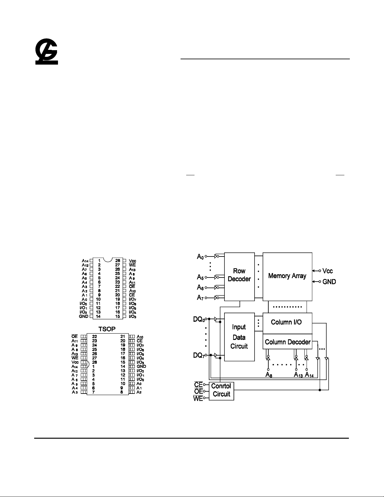
GLT725608 is high performance 256K bit static
random access memory organized as 32K by 8 bits
and operate at a single 5 volt supply. Fabricated with
G-Link Technology's very advanced CMOS submicron technology, GLT725608 offer a combination
of features: very high speed and very low stand-by
current. In addition, this device also supports easy
memory expansion with an active LOW chip enable
(CE) as well as an active LOW output enable (OE)
and three state outputs.
330 mil SOP Packages.
∗ Industrial Grade Available (-40°C ~ 85°C).
Pin Configurations : Function Block Diagram :
SOJ and SOP
G-Link Technology
2701 Northwestern Parkway
Santa Clara, CA 95051, U.S.A.
G-Link Technology Corporation, Taiwan
6F, No. 24-2, Industry E, RD, IV, Science Based
Industrial Park, Hsin Chu, Taiwan.
- 1 -
Page 2
G-LINK
CE
OE
WE
WECEOE
Pin Descriptions:
Name Function
A0 - A
I/O0 - I/O
V
14
7
CC
GND Ground
Truth Table:
Address Inputs
Chip Enable Input
Output Enable Input
Write Enable Input
Data Input and Data Output
+5V Power Supply
GLT725608
Ultra High Performance 32K x 8 Bit CMOS STATIC RAM
Feb, 2001(Rev.2.4)
Mode
Not Selected
X H X High Z
I/O Operation
(Power Down)
Output Disabled H L H High Z
Read H L L
Write L L X
Absolute Maximum Ratings:
Operation Range :
Range Temperature Vcc
Ambient Temperature
Under Bias...................................-10°C to
+80°C
Storage Temperature(plastic)....-55°C to
+125°C
Voltage Relative to GND.............-0.5V to +
7.0V
Data Output Current..................................50mA
Power Dissipation......................................1.0W
1.Stresses greater than those listed under ABSOLUTE
MAXIMUM RATING may cause permanent damage to the
device. This is a stress rating only and functional operation
of the device at these or any other conditions above those
indicated in the operational sections of this specification is
not implied. Exposure to absolute maximum rating
conditions for extended periods may affect reliability.
Commercial 0°C to + 70°C 5V ± 10%
Industrial -40°C to 85°C 5V ± 10%
Capacitance
(1)
TA=25°°C,f=1.0MHZ :
Sym. Parameter conditions Max. Unit
C
IN
C
I/O
Input
Capacitance
Input / output
Capacitance
D
OUT
D
IN
VIN = 0V 8 pF
V
= 0V 10 pF
I/O
V Current
CC
I , I
CCSB CCSB1
I
CC
I
CC
I
CC
G-Link Technology
2701 Northwestern Parkway
Santa Clara, CA 95051, U.S.A.
G-Link Technology Corporation, Taiwan
6F, No. 24-2, Industry E, RD, IV, Science Based
Industrial Park, Hsin Chu, Taiwan.
- 2 -
Page 3
G-LINK
CCSB1
CE
CCDR
(1)
Ultra High Performance 32K x 8 Bit CMOS STATIC RAM
DC Characteristics
Sym. Parameter Test Conditions Min. Typ
V
V
I
I
V
V
I
I
I
Guaranteed Input Low
IL
Voltage
Guaranteed Input High
IH
Voltage
Input Leakage Current VCC= Max., VIN=0V to V
LI
Output Leakage Current
LO
Output Low Voltage VCC= Min., IOL =8mA - - 0.4 V
OL
Output High Voltage VCC= Min., IOH =-4mA 2.4 - - V
OH
Operating Power Supply
CC
Current
Standby Power Supply
CCSB
Current
Power Down Power
Supply Current
(2)
(2)
CC
VCC= Max., CE≥V
VCC= Max., CE≤VIL,
I
=0mA., F= F
I/O
VCC= Max., CE≥VIH,
I
=0mA., F= F
I/O
max
max
IH
(3)
(3)
VCC= Max., CE≥VCC.-0.2V,
VIN≥VCC. -0.2V or
-0.3 - +0.8 V
2.2 - VCC+0.3 V
-5 - 5
-5 - 5
- - -12 -15 -20
- -
- - 10 10 10 mA
GLT725608
(1)
Max. Unit
160 150 120 mA
40 30 20 mA
Feb, 2001(Rev.2.4)
µA
µA
1. Typical characteristics are at VCC=5V, TA=25
2. These are absolute values with reject to device ground and all overshoots due to system or
tester noise are included.
3. F
MAX
=1/tRC.
Data Retention
Sym. Parameter Test Conditions Min. Typ
V
I
t
CDR
t
R
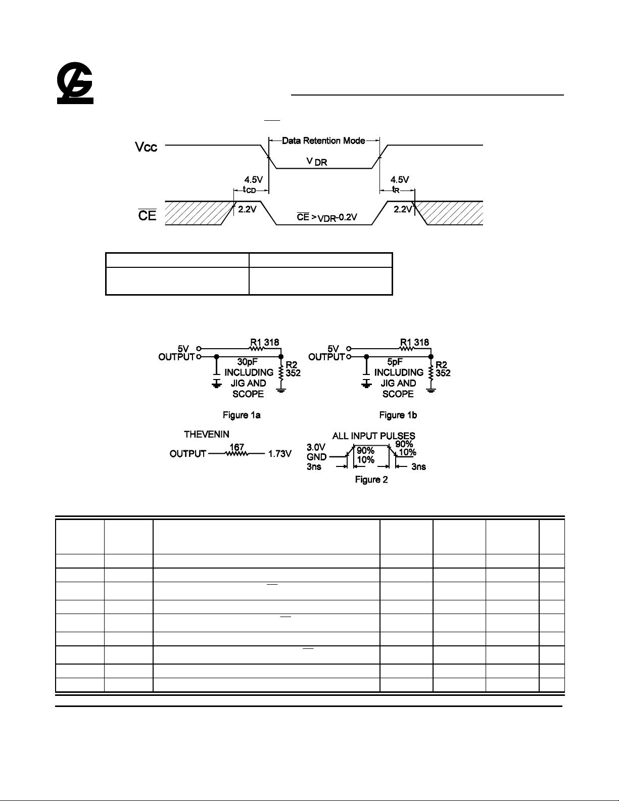
1. CE ≥ VDR -0.2V, VIN ≥ VDR -0.2V or VIN ≤ 0.2V.
2. tRC =Read Cycle Time.
VCC for Data retention
DR
≥ VCC -0.2V,
2.0 - 5.5 V
VIN ≥ VCC -0.2V or VIN ≤ 0.2V
Data Retention Current VDR=2.0V - 30
VDR=3.0V 50
Chip Deselect to Data
0 - - ns
Retention Time See Retention Waveform
Operating Recovery Time t
RC
(2)
(1)
Max. Unit
- - ns
µA
µA
G-Link Technology
2701 Northwestern Parkway
Santa Clara, CA 95051, U.S.A.
G-Link Technology Corporation, Taiwan
6F, No. 24-2, Industry E, RD, IV, Science Based
Industrial Park, Hsin Chu, Taiwan.
- 3 -
Page 4
G-LINK
Ultra High Performance 32K x 8 Bit CMOS STATIC RAM
Low VCC Data Retention Waveform (CE Controlled)
AC Test Conditions
Input Pulse Levels 0V to 3.0V
Input Rise and Fall Times
Timing Reference Level
AC Test Loads and Waveforms
3 ns
1.5V
GLT725608
Feb, 2001(Rev.2.4)
AC Electrical Characteristics
Read Cycle
JEDEC
Parameter
Name
t
AVAX
t
AVQV
t
E1LQV
t
GLQV
t
E1LQX
t
GLQX
t
E1HQZ
t
GHQZ
t
AXQX
Parameter
Name Parameter
t
t
t
t
t
t
RC
t
AA
ACS
t
OE
CLZ
OLZ
CHZ
OHZ
t
OH
Read Cycle Time
Address Access Time
Chip Select Access Time,
Output Enable to Output Valid
Chip Select to Output Low Z,
Output Enable to Output in Low Z
Chip Deselect to Output in High Z,
Output Disable to Output in High Z
Output Hold from Address Change
Ω
Ω
Ω
725608-12
Min. Max.
Ω
Ω
725608-15
Min. Max.
725608-20
Min. Max. Unit
12 - 15 - 20 - ns
- 12 - 15 - 20 ns
CE
- 12 - 15 - 20 ns
- 5 - 6 - 8 ns
CE
3 - 3 - 3 - ns
3 - 3 - 3 - ns
CE
- 7 - 8 - 10 ns
- 6 - 6 - 8 ns
3 - 3 - 3 - ns
G-Link Technology
2701 Northwestern Parkway
Santa Clara, CA 95051, U.S.A.
G-Link Technology Corporation, Taiwan
6F, No. 24-2, Industry E, RD, IV, Science Based
Industrial Park, Hsin Chu, Taiwan.
- 4 -
Page 5

G-LINK
WE
OE
GLT725608
Ultra High Performance 32K x 8 Bit CMOS STATIC RAM
Feb, 2001(Rev.2.4)
Switching Waveform (Read Cycle)
READ CYCLE 1
READ CYCLE 2
READ CYCLE 3
(1,2,4)
(1,3,4)
(1)
Notes:
1.
2. Device is continuously selected CE≤VIL.
3. Address valid prior to or coincident with CE transition low and/or transition high.
4.
5. Transition is measured ±200mV from steady state with CL=5pF.
G-Link Technology
2701 Northwestern Parkway
Santa Clara, CA 95051, U.S.A.
is High for READ Cycle.
≤VIL.
G-Link Technology Corporation, Taiwan
6F, No. 24-2, Industry E, RD, IV, Science Based
Industrial Park, Hsin Chu, Taiwan.
- 5 -
Page 6

G-LINK
AC Electrical Characteristics
Write Cycle
JEDEC
Parameter
Name
t
AVAX
t
E1LWH
t
AVWL
t
AVWH
t
WLWH
t
WHAX
t
E2LAX
t
WLQZ
t
DVWH
t
WHDX
t
WHQX
Parameter
Name Parameter
t
t
t
t
t
t
t
t
t
WC
CW
t
AS
AW
WP
WR1
WR2
WHZ
DW
t
DH
OW
Write Cycle Time
Chip Select to End of Write
Address Set up Time
Address Valid to End of Write
Write Pulse Width
Write Recovery Time,
Write Recovery Time,
Write to Output in High Z
Data to Write Time Overlap
Data Hold from Write Time
End of Write to Output Active
WE
CE
GLT725608
Ultra High Performance 32K x 8 Bit CMOS STATIC RAM
725608-12
Min. Max.
725608-15
Min. Max.
12 - 15 - 20 - ns
10 - 12 - 15 - ns
0 - 0 - 0 - ns
10 - 12 - 15 - ns
10 - 12 - 15 - ns
0 - 0 - 0 - ns
0 - 0 - 0 - ns
- 7 - 8 - 10 ns
6 - 7 - 8 - ns
0 - 0 - 0 - ns
3 - 3 - 3 - ns
Feb, 2001(Rev.2.4)
725608-20
Min. Max. Unit
Switching Waveforms(Write Cycle)
WRITE CYCLE 1
(1)
G-Link Technology
2701 Northwestern Parkway
Santa Clara, CA 95051, U.S.A.
G-Link Technology Corporation, Taiwan
6F, No. 24-2, Industry E, RD, IV, Science Based
Industrial Park, Hsin Chu, Taiwan.
- 6 -
Page 7

G-LINK
WE
WE
Switching Waveform (Write Cycle)
WRITE CYCLE 2
(1,6)
GLT725608
Ultra High Performance 32K x 8 Bit CMOS STATIC RAM
Feb, 2001(Rev.2.4)
Note:
1.
2. The internal write time of the memory is defined by the overlap CE low and WE low. All signals
3. TWR is measured from the earlier of CE or WE going high at the end of write cycle.
4. During this period, I/O pins are in the output state so that the input signals of opposite phase to
5. If the CE low transition occurs simultaneously with the WE low transitions or after the
6. OE is continuously low (OE=VIL).
7. D
8. D
9. If CE is low during this period, I/O pins are in the output state. Then the data input signals of
10. Transition is measured ±200mV from steady state with CL=5pF.
11. tCW is measured from CE going low to the end of write.
must be high during address transitions.
must be active to initiate a write and any one signal can terminate a write by going inactive. The
data input setup and hold timing should be referenced to the second transition edge of the
signal that terminates the write.
the outputs must not be applied.
transition, outputs remain in a high impedance state.
is the same phase of write data of this write cycle.
OUT
is the read data of next address.
OUT
opposite phase to the outputs must not be applied to them.
G-Link Technology
2701 Northwestern Parkway
Santa Clara, CA 95051, U.S.A.
G-Link Technology Corporation, Taiwan
6F, No. 24-2, Industry E, RD, IV, Science Based
Industrial Park, Hsin Chu, Taiwan.
- 7 -
Page 8

G-LINK
Part Number
SPEED
POWER
PACKAGE
GLT725608-12J3
12ns
Normal
SOJ 300mil 28L
GLT725608-15J3
15ns
Normal
SOJ 300mil 28L
GLT725608-20J3
20ns
Normal
SOJ 300mil 28L
GLT725608-12TS
12ns
Normal
TSOP 28L
GLT725608-15TS
15ns
Normal
TSOPI 28L
GLT725608-20TS
20ns
Normal
TSOPI 28L
GLT725608-12TC
12ns
Normal
TSOPII 28L
GLT725608-15TC
15ns
Normal
TSOPII 28L
GLT725608-20TC
20ns
Normal
TSOPII 28L
GLT725608-12FB
12ns
Normal
SOP 330mil 28L
GLT725608-15FB
15ns
Normal
SOP 330mil 28L
GLT725608-20FB
20ns
Normal
SOP 330mil 28L
Ordering Information
Parts Numbers (Top Mark) Definition :
GLT725608
Ultra High Performance 32K x 8 Bit CMOS STATIC RAM
Feb, 2001(Rev.2.4)
GLT 7 256 08 I - 12 TC
4 : DRAM
6 : Standard
SRAM
7 : Cache SRAM
8 : Synchronous
Burst SRAM
-SRAM
064 : 8K
256 : 256K
512 : 512K
100 : 1M
-DRAM
10 : 1M(C/EDO)*
11 : 1M(C/FPM)*
12 : 1M(H/EDO)*
13 : 1M(H/FPM)*
20 : 2M(EDO)
21 : 2M(FPM)
40 : 4M(EDO)
41 : 4M(FPM)
80 : 8M(EDO)
81 : 8M(FPM)
160 : 16M(EDO)
161 : 16M(FPM)
CONFIG.
04 : x04
08 : x08
16 : x16
32 : x32
VOLTAGE
Blank : 5V
L : 3.3V
M : 2.5V
N : 2.1V
SPEED
-SRAM
12 : 12ns
15 : 15ns
20 : 20ns
70 : 70ns
-DRAM
35 : 35ns
40 : 40ns
45 : 45ns
50 : 50ns
60 : 60ns
Temperature Range
E : Extended Temperature
I : Industrial Temperature
Blank : Commercial Temperature
PACKAGE
T : PDIP(300mil)
TS : TSOP(Type I)
TC : TSOP(Type ll)
PL : PLCC
FA : 300mil SOP
FB : 330mil SOP
FC : 445mil SOP
J3 : 300mil SOJ
J4 : 400mil SOJ
P : PDIP(600mil)
Q : PQFP
TQ : TQFP
G-Link Technology
2701 Northwestern Parkway
Santa Clara, CA 95051, U.S.A.
G-Link Technology Corporation, Taiwan
6F, No. 24-2, Industry E, RD, IV, Science Based
Industrial Park, Hsin Chu, Taiwan.
- 8 -
Page 9

G-LINK
Package Information
300mil 28 Lead Small Outline J-form Package (SOJ)
GLT725608
Ultra High Performance 32K x 8 Bit CMOS STATIC RAM
Feb, 2001(Rev.2.4)
G-Link Technology
2701 Northwestern Parkway
Santa Clara, CA 95051, U.S.A.
G-Link Technology Corporation, Taiwan
6F, No. 24-2, Industry E, RD, IV, Science Based
Industrial Park, Hsin Chu, Taiwan.
- 9 -
Page 10

G-LINK
Ultra High Performance 32K x 8 Bit CMOS STATIC RAM
28L (8×13.4 mm) Thin Small Outline Package (TSOP) Type I
GLT725608
Feb, 2001(Rev.2.4)
G-Link Technology
2701 Northwestern Parkway
Santa Clara, CA 95051, U.S.A.
G-Link Technology Corporation, Taiwan
6F, No. 24-2, Industry E, RD, IV, Science Based
Industrial Park, Hsin Chu, Taiwan.
- 10 -
Page 11

G-LINK
Ultra High Performance 32K x 8 Bit CMOS STATIC RAM
28L (8×20mm) Thin Small Outline Package (TSOP) Type I
GLT725608
Feb, 2001(Rev.2.4)
G-Link Technology
2701 Northwestern Parkway
Santa Clara, CA 95051, U.S.A.
G-Link Technology Corporation, Taiwan
6F, No. 24-2, Industry E, RD, IV, Science Based
Industrial Park, Hsin Chu, Taiwan.
- 11 -
Page 12

G-LINK
Ultra High Performance 32K x 8 Bit CMOS STATIC RAM
330mil 28 Lead Thin Small Outline (Gull-Wing) Package (SOP)
GLT725608
Feb, 2001(Rev.2.4)
G-Link Technology
2701 Northwestern Parkway
Santa Clara, CA 95051, U.S.A.
G-Link Technology Corporation, Taiwan
6F, No. 24-2, Industry E, RD, IV, Science Based
Industrial Park, Hsin Chu, Taiwan.
- 12 -
 Loading...