

Page 1
PHOTODIODE
InGaAs PIN photodiode array
G8909-01
Photodiode array for DWDM monitor
Features
l
250 µm pitch, 40 ch parallel readout
l
Low cross-talk
l
Precise chip position tolerance: ±0.05 mm
Applications
l
DWDM monitor with AWG
■ General ratings
Parameter Value Unit
Active area f0.08 mm
Pixel pitch 250 µm
Number of elements 40 ch
■ Absolute maximum ratings
Parameter Symbol Remark Value Unit
Reverse voltage VR Max
Allowable input power P
Operating temperature Topr -40 to +85 °C
Storage temperature Ts tg
* In N environment or in vacuum
.
Max. 10 mV
in
*
6V
-40 to +85 °C
■ Electrical and optical characteristics (Ta=25 °C, per 1 element)
Parameter Symbol Condition Min. Typ . Max. Unit
Spectral response range l - 0.9 to 1.7 - µm
Photo sensitivity S
Photo response non-uniformity PRNU - - ±5 %
Dark current I
Shunt resistance Rsh VR=10 mV - 8 - GW
Terminal capacitance Ct VR=5 V, f=1 MHz - 1.4 - pF
Cross-talk - VR=0.1 V - -33 - dB
PRELIMINARY DATA
Apr. 2002
l=1.31 µm
l=1.55 µm
VR=5 V - 0.02 0.2 nA
D
0.8 0.9 -
0.85 0.95 -
A/W
1
Page 2
InGaAs PIN photodiode array
G8909-01
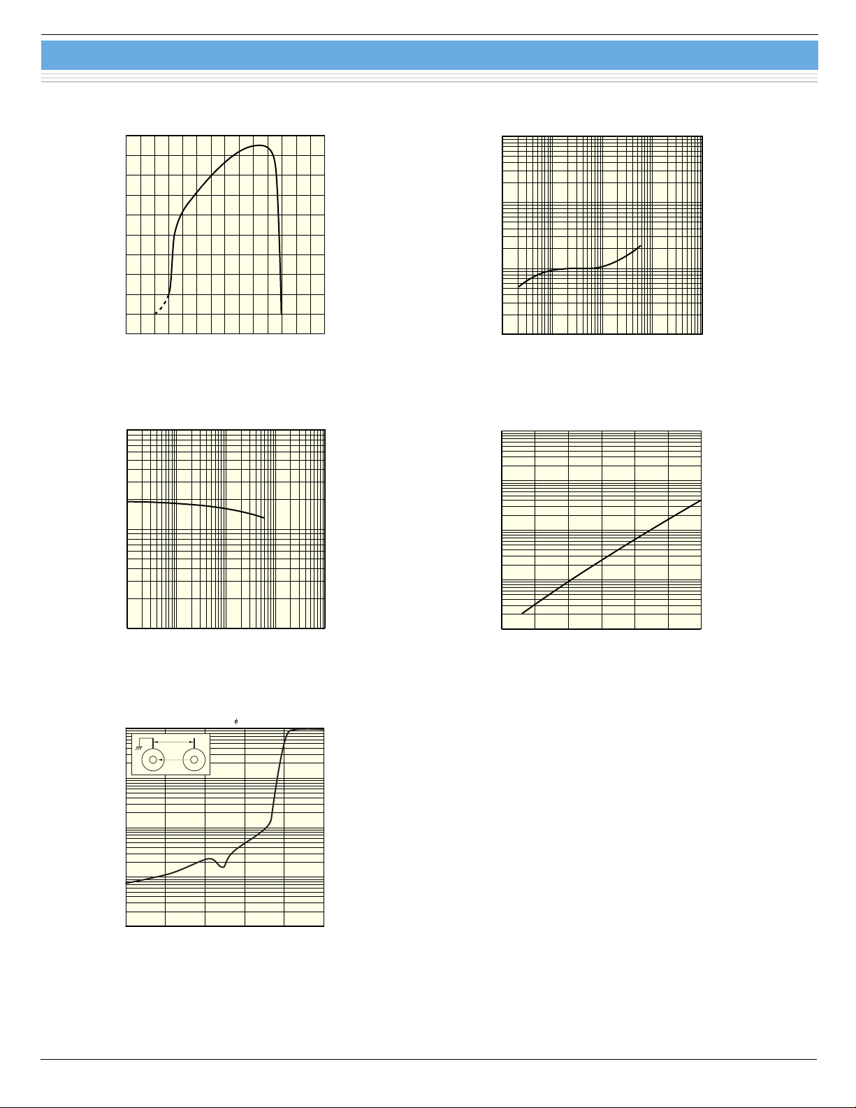
■ Spectral response
1
0.5
PHOTO SENSITIVITY (A/W)
0.8 1.0 1.2 1.4 1.6 1.8
0.6
WAVELENGTH (µm)
(Typ. Ta=25 ˚C)
2.0
■ Terminal capacitance vs. reverse voltage
10 pF
(Typ. Ta=25 ˚C, f=1 MHz)
KIRDB0002EB
■ Dark current vs. reverse voltage
1 nA
100 pA
10 pA
DARK CURRENT
1 pA
0.01 0.1 1
REVERSE VOLTAGE (V)
(Typ. Ta=25 ˚C)
■ Dark current vs. temperature
100 nA
10 nA
10
(Typ. V
R
=5 V)
100
KIRDB0266EA
1 pF
TERMINAL CAPACITANCE
100 fF
0.01 0.1 1
REVERSE VOLTAGE (V)
■ Cross-talk characteristic
(Typ. Ta=25 ˚C, λ=1.55 µm, SPOT= 20 µm, Pin=5 nW, VR=0.1 V)
100
250 µm
10
1
0.1
RELATIVE SENSITIVITY (%)
0.01
-250 -200 -100
1 nA
DARK CURRENT
100 pA
10
100
10 pA
20 30 50
7040 60
80
TEMPERATURE (˚C)
KIRDB0267EA KIRDB0268EA
-50-150
0
POSITION X (µm)
KIRDB0269EA
2
Page 3

■ Dimensional outline (unit: mm)
ANODE PAD
(PITCH: 400 µm, 40 ch,
150 × 150 µm BOND PADS)
22.0
2.1
(0.1)
0.4
InGaAs PIN photodiode array
CATHODE PAD
0.80.5
G8909-01
2.52.0
10.5
DETAIL a
a
0.80
(0.15)
0.70 ± 0.05 *
* The center of the active area
to the bottom of the substrate
KIRDA0158EA
Information furnished by HAMAMATSU is believed to be reliable. However, no responsibility is assumed for possible inaccuracies or omissions.
HAMAMATSU PHOTONICS K.K., Solid State Division
1126-1 Ichino-cho, Hamamatsu City, 435-8558 Japan, Telephone: (81) 053-434-3311, Fax: (81) 053-434-5184, http://www.hamamatsu.com
U.S.A.: Hamamatsu Corporation: 360 Foothill Road, P.O.Box 6910, Bridgewater, N.J. 08807-0910, U.S.A., Telephone: (1) 908-231-0960, Fax: (1) 908-231-1218
Germany: Hamamatsu Photonics Deutschland GmbH: Arzbergerstr. 10, D-82211 Herrsching am Ammersee, Germany, Telephone: (49) 08152-3750, Fax: (49) 08152-2658
France: Hamamatsu Photonics France S.A.R.L.: 8, Rue du Saule Trapu, Parc du Moulin de Massy, 91882 Massy Cedex, France, Telephone: 33-(1) 69 53 71 00, Fax: 33-(1) 69 53 71 10
United Kingdom: Hamamatsu Photonics UK Limited: 2 Howard Court, 10 Tewin Road, Welwyn Garden City, Hertfordshire AL7 1BW, United Kingdom, Telephone: (44) 1707-294888, Fax: (44) 1707-325777
North Europe: Hamamatsu Photonics Norden AB: Smidesvägen 12, SE-171 41 Solna, Sweden, Telephone: (46) 8-509-031-00, Fax: (46) 8-509-031-01
Italy: Hamamatsu Photonics Italia S.R.L.: Strada della Moia, 1/E, 20020 Arese, (Milano), Italy, Telephone: (39) 02-935-81-733, Fax: (39) 02-935-81-741
Specifications are subject to change without notice. No patent rights are granted to any of the circuits described herein. ©2003 Hamamatsu Photonics K.K.
Cat. No. KIRD1053E02
Feb. 2003 DN
3
 Loading...