

Page 1
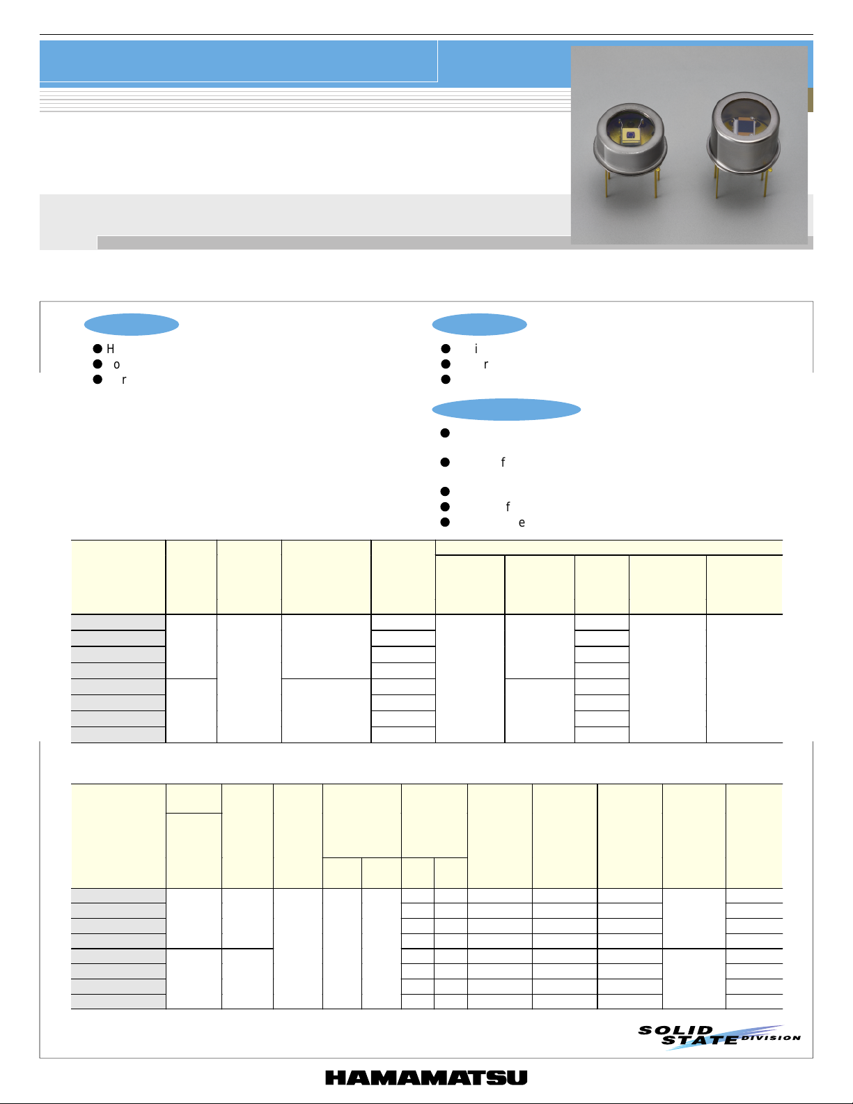
PHOTODIODE
InGaAs PIN photodiode
G8605 series
Thermoelectrically cooled NIR (near infrared) detector with low noise and high-speed response
InGaAs PIN photodiodes have small terminal capacitance for high-speed response and also feature high shunt resistance and very low noise.
G8605 series of InGaAs PIN photodiodes are thermoelectrically cooled types that decrease the dark current to achieve high D*. One-stage (-10 ˚C)
and two-stage (-20 ˚C) thermoelectrically cooled types are provided.
Features
l
High-speed response
l
Low noise
l
Various active area sizes available from φ1 to φ5 mm
Specifications / Absolute maximum ratings
■
Dimensional
Type No.
G8605-11
G8605-12
G8605-13
G8605-15
G8605-21
G8605-22
G8605-23
G8605-25
outline/
Window
m aterial *
/K
➀
/K
➁
Package Cooling
One-stage
TE-cooled
TO-8
Two-stage
TE-cooled
Applications
l
Optical power meter
l
Water content analyzer
l
Laser diode life test
Accessories (Optional)
l
Preamp for InGaAs PIN photodiode C4159-02
(High-speed type)
l
Preamp for InGaAs PIN photodiode C4159-03
(High sensitivity type)
l
Heatsink for one-stage TE-cooled type A3179
l
Heatsink for two-stage TE-cooled type A3179-01
l
Temperature controller for TE-cooled type C1103-04
Absolute maximum ratings
Active
area
(mm) (mW) (A) (V) (°C) (°C)
φ
φ
φ
φ
φ
φ
φ
φ
1
2
3
5
1
2
3
5
Thermistor
power
dissipation
0.2
TE-cooler
allowable
current
1.5
1.0
Reverse
voltage
Max.
V
R
5
5
5
2
5
5
5
2
Operating
temperature
Topr
-40 to +70 -55 to +85
Storage
temperature
Tstg
Electrical and optical characteristics (Typ. unless otherwise noted)
■
Measurement
condition
Type No.
G8605-11
G8605-12
G8605-13
G8605-15
G8605-21
G8605-22
G8605-23
G8605-25
* Window material K: borosilicate glass with anti-reflective coating (optimized for 1.55 µm peak)
Element
tem perature
(°C) (µm) (µm)
-10
-20
Spectral
response
range
λ
0.9 to 1.67
0.9 to 1.65
Peak
se nsitivity
wavelength
p
λ
1.55
Photo
sensitivity
S
1.3 µm
(A/W )
(A/W )
0.9 0.95
λ=λ
Dark current
I
D
VR=1 V
p
Typ.
Max.
(nA )
0.07 0.35
0.3 1.5
15
2.5 12.5
0.03 0.15
0.15 0.75
0.5 2.5
1.2 6
(nA )
Cut-off
frequency
fc
VR=1 V
=50
R
L
(MHz) (pF)
18 150 1500 5 × 10
4 550 300 1 × 10
2 1000 100 2 × 10
0.6 3500 30
18 150 3000 3 × 10
4 550 600 7 × 10
2 1000 200 1 × 10
0.6 3500 60
Ω
Terminal
capacitance
Ct
VR=1 V
f=1 MHz
Shunt
resistance
Rsh
VR=10 mV
(MΩ)
D
λ=λ
(cm ·Hz
2 × 10
3 × 10
∗
1/2
p
/W )
13
13
NEP
λ=λ
(W/Hz
3 × 10
2 × 10
p
1/2
)
-15
-14
-14
-14
-15
-15
-14
-14
1
Page 2
InGaAs PIN photodiode
100 nA
0.01 0.1 1 10 100
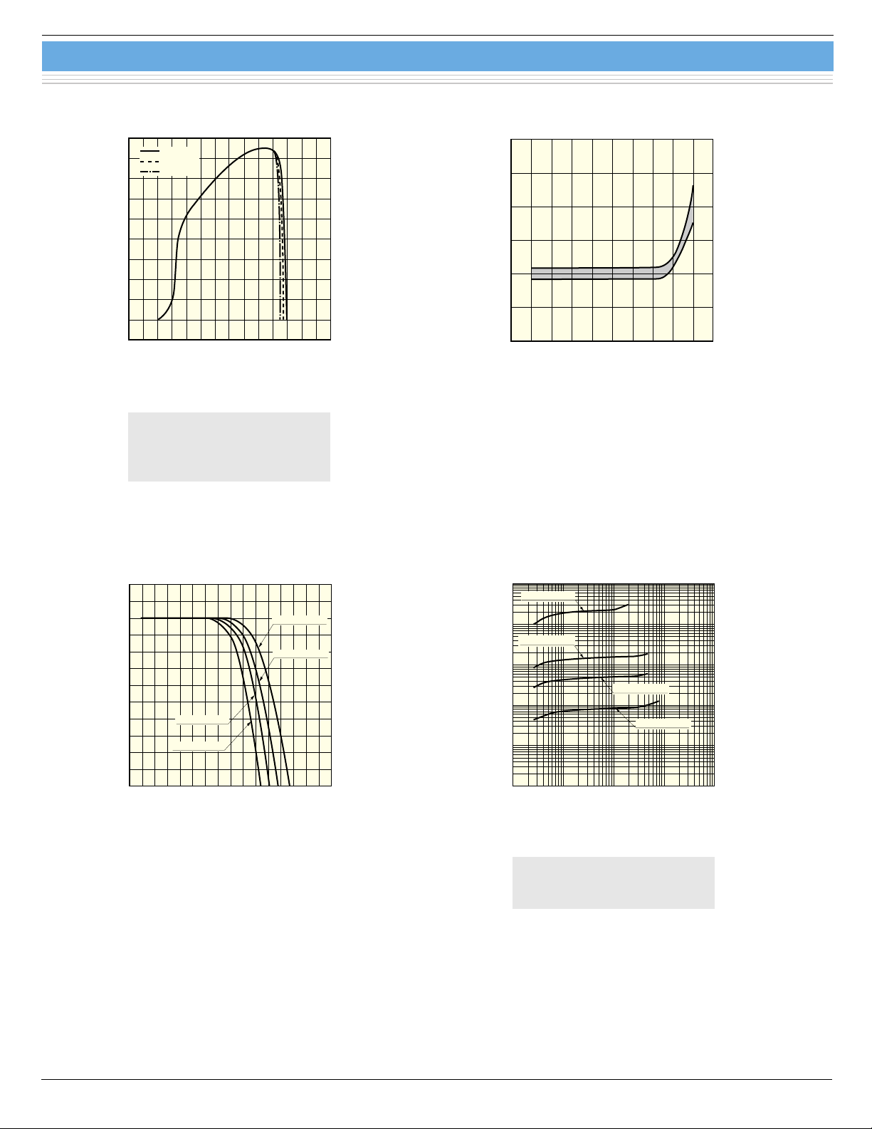
REVERSE VOLTAGE (V)
DARK CURRENT
10 nA
100 pA
10 pA
1 nA
1 µA
(Typ. Ta=25
˚C
)
G8605-15/-25
G8605-13/-23
G8605-12/-22
G8605-11/-21
G8605 series
■
Spectral response
1
T=25 ˚C
T= -10 ˚C
T= -20 ˚C
0.5
PHOTO SENSITIVITY (A/W)
0.8 1.0 1.2 1.4 1.6 1.8
0.6
Spectral response shifts towards the
short wavelength side when cooled.
One-stage TE-cooled type: λc=1.67 µm
Two-stage TE-cooled type: λc=1.65 µm
WAVELENGTH (µm)
(Typ.)
2.0
KIRDB0184EA
■
Photo sensitivity temperature characteristic
2
1
0
(Typ. Ta=25
˚C
TEMPERATURE COEFFICIENT (%/˚C)
-1
1.0 1.2 1.4 1.6 1.80.8
WAVELENGTH (µm)
)
KIRDB0042EA
■
Photo sensitivity linearity
˚C
102
100
98
96
94
RELATIVE SENSITIVITY (%)
92
90
(Typ. Ta=25
G8605-13/-23
G8605-15/-25
02 6 1012 16
48 14
INCIDENT LIGHT LEVEL (mW)
, λ=1.3 µm, RL=2 Ω, VR=0 V)
G8605-11/-21
G8605-12/-22
KIRDB0241EA
■
Dark current vs. reverse voltage
Applying a reverse voltage increases
dark current, but improves frequency
characteristics and output linearity.
KIRDB0242EA
2
Page 3

InGaAs PIN photodiode
G8605 series
■
Terminal capacitance vs. reverse voltage
˚C
10 nF
1 nF
G8605-12/-22
100 pF
10 pF
TERMINAL CAPACITANCE
G8605-11/-21
1 pF
0.01 0.1 1 10 100
(Typ. Ta=25
, f=1 MHz)
G8605-15/-25
G8605-13/-23
REVERSE VOLTAGE (V)
In applications requiring high-speed
response, the lead length should be as
short as possible to minimize the terminal capacitance.
■
Thermistor temperature characteristic
6
10
■
Shunt resistance vs. element temperature
R
=10 mV)
10 GΩ
1 GΩ
100 MΩ
10 MΩ
G8605-13/-23
SHUNT RESISTANCE
1 MΩ
100 kΩ
G8605-15/-25
-40 -20 0 40 60 80
(Typ. V
G8605-11/-21
G8605-12/-22
20
ELEMENT TEMPERATURE (˚C)
KIRDB0243EA KIRDB0244EA
■
Cooling characteristics of TE-cooler
(Typ.)
(Typ. Ta=25 ˚C, Thermal resistance of heatsink=3 ˚C/W)
40
5
10
4
10
RESISTANCE (Ω)
3
10
-40 -20 0 20
ELEMENT TEMPERATURE (˚C)
KIRDB0116EA KIRDB0231EA
■
Current vs. voltage characteristics of TE-cooler
(Typ. Ta=25 ˚C, Thermal resistance of heatsink=3 ˚C/W)
1.6
1.4
1.2
ONE-STAGE
TE-COOLED TYPE
1.0
0.8
0.6
CURRENT (A)
0.4
0.2
TWO-STAGE
TE-COOLED TYPE
20
ONE-STAGE
TE-COOLED TYPE
0
-20
TWO-STAGE
TE-COOLED TYPE
-40
ELEMENT TEMPERATURE (˚C)
-60
0 0.4 0.8 1.2 1.6
CURRENT (A)
0
0 0.5 1.0 1.5
VOLTAGE (V)
KIRDB0115EA
3
Page 4

■
Dimensional outlines (unit: mm)
15.3 ± 0.2
14 ± 0.2
WINDOW
10 ± 0.2
6.4 ± 0.212 MIN.
4.4 ± 0.2
InGaAs PIN photodiode
➁ G8605-21/-22/-23/-25➀ G8605-11/-12/-13/-15
15.3 ± 0.2
14 ± 0.2
WINDOW
10 ± 0.2
G8605 series
10 ± 0.212 MIN.
6.7 ± 0.2
PHOTOSENSITIVE
SURFACE
0.45
LEAD
5.1 ± 0.2
5.1 ± 0.2
10.2 ± 0.2
DETECTOR (ANODE)
DETECTOR (CATHODE)
TE-COOLER (-)
TE-COOLER (+)
THERMISTOR
KIRDA0152EA KIRDA0153EA
PHOTOSENSITIVE
SURFACE
0.45
LEAD
5.1 ± 0.2
5.1 ± 0.2
10.2 ± 0.2
DETECTOR (ANODE)
DETECTOR (CATHODE)
TE-COOLER (-)
TE-COOLER (+)
THERMISTOR
Information furnished by HAMAMATSU is believed to be reliable. However, no responsibility is assumed for possible inaccuracies or omissions.
HAMAMATSU PHOTONICS K.K., Solid State Division
1126-1 Ichino-cho, Hamamatsu City, 435-8558 Japan, Telephone: (81) 053-434-3311, Fax: (81) 053-434-5184, http://www.hamamatsu.com
U.S.A.: Hamamatsu Corporation: 360 Foothill Road, P.O.Box 6910, Bridgewater, N.J. 08807-0910, U.S.A., Telephone: (1) 908-231-0960, Fax: (1) 908-231-1218
Germany: Hamamatsu Photonics Deutschland GmbH: Arzbergerstr. 10, D-82211 Herrsching am Ammersee, Germany, Telephone: (49) 08152-3750, Fax: (49) 08152-2658
France: Hamamatsu Photonics France S.A.R.L.: 8, Rue du Saule Trapu, Parc du Moulin de Massy, 91882 Massy Cedex, France, Telephone: 33-(1) 69 53 71 00, Fax: 33-(1) 69 53 71 10
United Kingdom: Hamamatsu Photonics UK Limited: 2 Howard Court, 10 Tewin Road, Welwyn Garden City, Hertfordshire AL7 1BW, United Kingdom, Telephone: (44) 1707-294888, Fax: (44) 1707-325777
North Europe: Hamamatsu Photonics Norden AB: Smidesvägen 12, SE-171 41 Solna, Sweden, Telephone: (46) 8-509-031-00, Fax: (46) 8-509-031-01
Italy: Hamamatsu Photonics Italia S.R.L.: Strada della Moia, 1/E, 20020 Arese, (Milano), Italy, Telephone: (39) 02-935-81-733, Fax: (39) 02-935-81-741
Specifications are subject to change without notice. No patent rights are granted to any of the circuits described herein. ©2001 Hamamatsu Photonics K.K.
4
Cat. No. KIRD1049E01
Apr. 2001 DN
 Loading...