

Page 1
Global Mixed-mode Technology Inc.
Dual-Slot PCMCIA/CardBus Power Controller
Features
Backward Compatible with G570
Fully Integrated VCC and Vpp Switching for Dual
Slot PC Card
3-Lead Serial Interface Compatible With
CardBus
3.3V Low Voltage Mode
Meets PC Card Standards
RESET for System Initialization of PC Cards
12V Supply Can Be Disabled Except During
TM
Interface
TM
Controllers
12V Flash Programming
Short Circuit and Thermal Protection
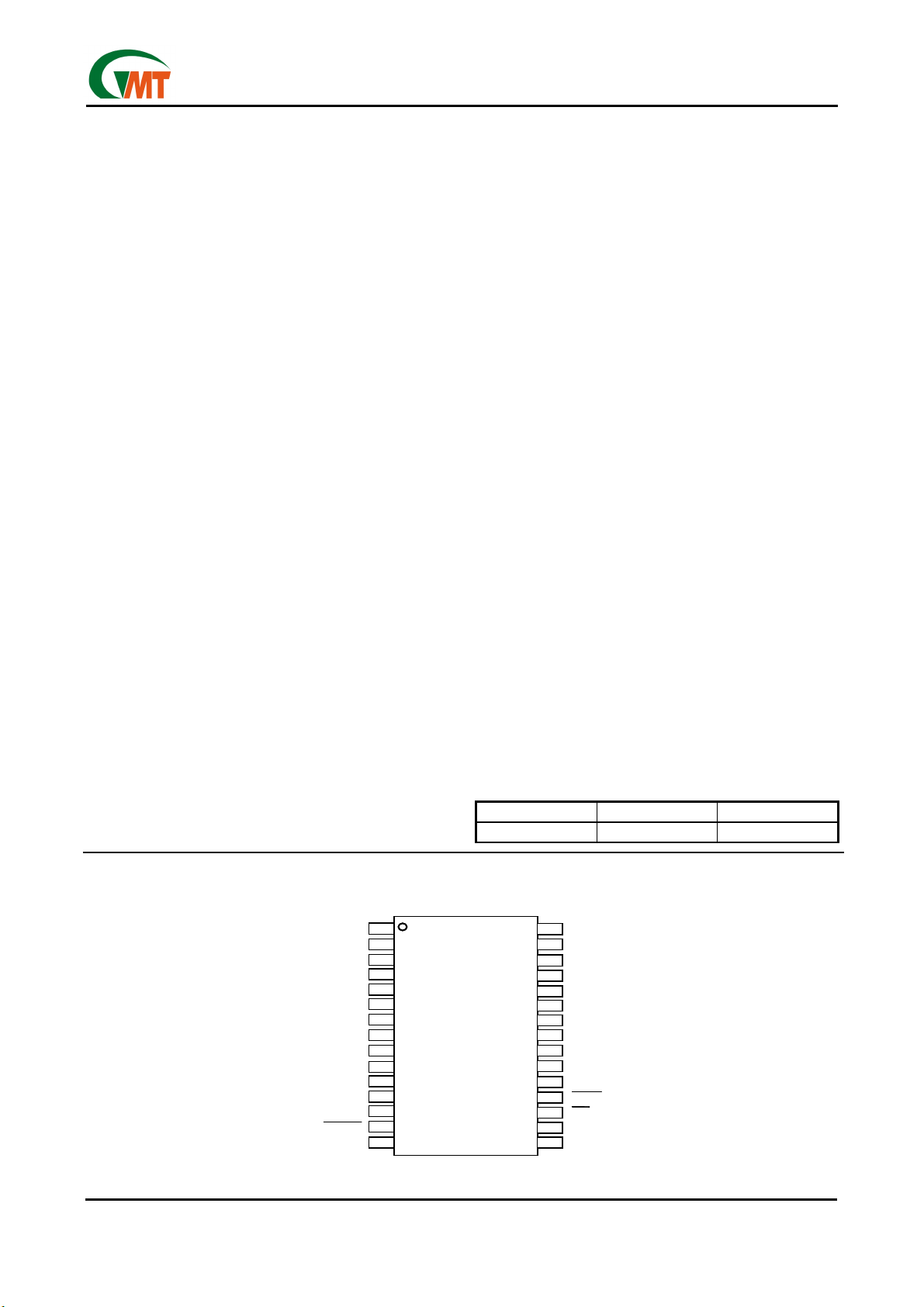
30 Pin SSOP
Compatible With 3.3V, 5V and 12V PC Cards
Low R
130 m
Break-Before-Make Switching
Internal power-On Reset
Standby mode: 60mA current limit (TYP)
DS(on)
3.3V V
ΩΩΩΩ
(180-m
CC
5V VCC Switch;
ΩΩΩΩ
Switch)
Application
Notebook PC
Electronic Dictionary
POS
Description
The G574 PC Card power-interface switch provides an
integrated power-management solution for two PC Cards.
All of the discrete power MOSFETs, a logic section, current limiting, and thermal protection for PC Card control
are combined on a single integrated circuit (IC). The circuit allows the distribution of 3.3V, 5V, and/or 12V card
power by means of the Serial interface. The current-
limiting feature eliminates the need for fuses, which reduces component count and improves reliability.
The G574 features a 3.3V low voltage mode that allows
for 3.3V switching without the need for 5V supply. This
facilitates low power system designs such as sleep
mode and pager mode where only 3.3V is available.
The G574 incorporates a reset function, selectable by
one of two inputs, to help alleviate system errors. The
reset function enables PC card initialization concurrent
with host platform initialization, allowing a system reset.
Reset is accomplished by grounding the V
(flash-memory programming voltage) outputs, which
discharges residual card voltage.
This device also has the ability to program the xVpp
outputs independent of the xVCC outputs. A standby
mode that changes all output-current limits to 50mA
(typical) has been incorporated.
G574
and VPP
CC
Pin Configuration
5V
5V
5V
5V
DATA
DATA
CLOCK
CLOCK
LATCH
LATCH
RESET
RESET
12V
12V
AVPP
AVPP
AVCC
AVCC
AVCC
AVCC
AVCC
AVCC
GND
GND
NC
NC
RESET
RESET
3.3V
3.3V
11
12
12
13
13
14
14
10
10
11
1
1
2
2
3
3
4
4
5
5
6
6
7
7
8
8
9
9
End equipment for the G574 includes notebook computers, desktop computers, personal digital assistants
(PDAs), digital cameras and bar-code scanners
The G574 is backward-compatible with the G570.
Ordering Information
PART NUMBER TEMP. RANGE PACKAGE
G574
G574
30Pin SSOP
30Pin SSOP
.
G574SA -40°C to +85°C 30 SSOP
5V
5V
30
30
MODE
MODE
29
29
NC
NC
28
28
NC
NC
27
27
NC
NC
26
26
NC
NC
25
25
12V
12V
24
24
23
23
BVPP
BVPP
22
22
BVCC
BVCC
21
21
BVCC
BVCC
20
20
BVCC
BVCC
STBY
STBY
19
19
18
18
OC
OC
3.3V
3.3V
17
17
3.3V
3.3V
1615
1615
Ver: 1.0
Jan 23, 2003
1
TEL: 886-3-5788833
http://www.gmt.com.tw
Page 2
Global Mixed-mode Technology Inc.
Absolute maximum ratings over operating
free-air temperature
Input voltage range for card power:
V
........…….......................………………-0.3V to 6V
I(3.3V)
V
……......................………..…...………..-0.3V to 6V
I(5V)
V
I(12V)…….
Logic input voltage...................................…-0.3V to 6V
Output current (each card):
I
O (xVCC)…………..
I
O(xVPP).
...................………..…………….. -0.3V to 14V
…………………..…...…..internally limited
................……............…........... internally limited
(unless otherwise noted)*
Operating virtual junction temperature range, T
……………………………………………….-40°C to 125°C
Operating free-air temperature range, T
...…………………….……..……………….-40°C to 85°C
Storage temperature range, T
Thermal resistance
SSOP 30………………………………………….122°C/W
Power dissipation P
SSOP 30…………………………………………1024mW
ESD…………………………..………………………Note1
….…...-55°C to 150°C
STG
θ
JA
+25°C)
(T
≤
D
A
G574
J
A
*Stresses beyond those listed under "absolute maximum ratings”may cause permanent damage to the device. These are stress rating
only, and functional operation of the device at these or any other conditions beyond those indicated under "recommended operating
conditions”is not implied. Exposure to absolute–maximum-rated conditions for extended periods may affect device reliability.
Note 1: ESD (electrostatic discharge) sensitive device. Proper ESD precautions are recommended to avoid performance degradation or
less of functionality.
Recommended Operating Conditions
V
2.7 5.25 V
I (5V)
Input voltage range, VI
Output current
Clock frequency 0 2.5 MHz
Operating virtual junction temperature, TJ -40 125 °C
V
2.7 5.25 V
I (3.3V)
13.5 V
V
I (12V)
I
at 25°C 1 A
O (xVCC)
I
at 25°C 150 mA
O (xVPP)
Min Max Unit
Typical PC Card Power-Distribution Application
AVCC
AVCC
AVCC
12V
12V
5V
5V
(Ce ram ic)
(Ce ram ic)
3.3V
3.3V
(Cera m ic)
(Cera m ic)
0.1µF
0.1µF
(Cera m ic)
(Cera m ic)
0.1µF
0.1µF
0.1µF
0.1µF
10µF
10µF
33µF
33µF
33µF
33µF
12V
12V
12V
12V
5V
5V
5V
5V
5V
5V
3.3V
3.3V
3.3V
3.3V
3.3V
3.3V
MODE
MODE
STBY
STBY
G574
G574
GND
GND
AVCC
AVCC
AVCC
BVCC
BVCC
BVCC
BVCC
BVCC
BVCC
AVPP
AVPP
BVPP
BVPP
DATA
DATA
CLOCK
CLOCK
LATCH
LATCH
RESET
RESET
RESET
RESET
OC
OC
0.1µF
0.1µF
0.1µF
0.1µF
0.1µF
0.1µF
0.1µF
0.1µF
System Voltage
System Voltage
Supervisor
Supervisor
or
or
PCI Bus Reset
PCI Bus Reset
V
V
CC
CC
V
V
CC
CC
Connector A
Connector A
V
V
PP1
PP1
V
V
PP2
PP2
V
V
CC
CC
V
V
CC
CC
V
V
PP1
PP1
V
V
PP2
PP2
DATA
DATA
CLOCK
CLOCK
LATCH
LATCH
GPI/O
GPI/O
PC Card
PC Card
PC Card
PC Card
Connector B
Connector B
PCMCIA
PCMCIA
C ontr olle r
C ontr olle r
Ver: 1.0
Jan 23, 2003
2
TEL: 886-3-5788833
http://www.gmt.com.tw
Page 3
Global Mixed-mode Technology Inc.
G574
Terminal Functions
TERMINAL
NAME NO.
3.3V 15,16,17 I 3.3V VCC input for card power
5V 1,2,30 I 5V VCC input for card power and/or chip power
12V 7,24 I 12V VPP input for card power
AVCC 9,10,11 O Switched output that delivers 0V, 3.3V, 5V or high impedance to card
AVPP 8 O Switched output that delivers 0V, 3.3V, 5V, 12V or high impedance to card
BVCC 20,21,22 O Switched output that delivers 0V, 3.3V, 5V or high impedance
BVPP 23 O Switch output that delivers 0V, 3.3V, 5V, 12V or high impedance
GND 12 Ground
MODE 29 I G570 operation when floating or pulled low; must be pulled high externally for G574 operation.
OC
RESET 6 I
RESET
STBY
CLOCK 4 I Logic level clock for serial data word
DATA 3 I Logic level serial data word
LATCH 5 I Logic level latch for serial data word
NC
18 O
14 I Logic-level reset input active low. Do not connect if RESET pin is used. The pin is internally
19 Logic-level active low input sets the G574 to standby mode and sets all current limits to 50mA.
13,25,26,
27,28
I/O DESCRIPTION
MODE is internally pulled low with a 150kΩ pulldown resistor.
Logic-level overcurrent. reports output that goes low when an overcurrent condition exists
Logic-level reset input active high. Do not connect if
pulled low with a 150kΩ pulldown resistor.
pulled high with a 150kΩ pullup resistor to 5V, if 5V V
exists only.
The pin is internally pulled high with a 150kΩ pullup resistor to 5V, if 5V V
to 3.3V, if 3.3V V
No internal connection
exists only.
CC
RESET
pin is used. RESET is internally
exists. And pulled to 3.3V, if 3.3V VCC
CC
exists. And pulled
CC
Ver: 1.0
Jan 23, 2003
3
TEL: 886-3-5788833
http://www.gmt.com.tw
Page 4
Global Mixed-mode Technology Inc.
Electrical Characteristics
(T
A=TJ
=25°C, V
I(5V)
=5V, V
I(3.3V)
=3.3V, V
I(12V)
=12V,
floating, all outputs unloaded (unless otherwise noted)
STBY
G574
DC Characteristics
PARAMETER TEST CONDITIONS MIN TYP MAX UNIT
5V to xVCC 150 180
3.3V to xVCC V
3.3V to xVCC V
I(5V)
I(5V)
= 5V, V
= 0V, V
=3.3V 100 130
I(3.3V)
=3.3V 110 150
I(3.3V)
5V to xVPP 3 4
Switch resistance*
3.3V to xVPP 2.9 4
12V to xVPP 1.3 2
3.3V/5V to xVCC 1.2 2
3.3V/5V to xVPP 12 12.5
12V to xVPP
V
Clamp low voltage IPP at 10mA 0.18 0.8 V
O(xVPP)
V
Clamp low voltage ICC at 10mA 0.13 0.8 V
O(xVCC)
I
Leakage current
IKG
IPP high impedance State
high-impedance State
I
CC
Normal operation
and in reset mode
I
Input current⊙
I
Shutdown mode
I
O(xVCC)
I
O(xVPP)
I
Short-circuit*
OS
Output current Limit
Standby mode, 3.3V to xVCC
Standby mode, 5V to xVCC
Standby mode, 3.3V to xVPP
Standby mode, 5V to xVPP
Standby mode, 12V to xVPP
Thermal shutdown※
Trip point, TJ
Hysteresis
STBY
= low, IO = 30mA
5 6.5
= 25°C 0.3 1
T
A
= 25°C 0.3 1
T
A
I
6 15
I(3.3V)
= V
V
I
110 150
O(xVCC)
I(5V)
I
I(12V)
I
82 150
I(3.3V)
I
I(5V)
I
I(12V)
I
I(3.3V)
I
I(5V)
I
I(12V)
= 0, V
V
I(5V)
0
V
O(xVPP)
= 12V
1
V
O(xVCC)
= Hi-Z, V
2 10
Output powered into a short to
GND
O(xVCC)
O(xVCC)
= 5V
= 3.3V
O(xVPP)
5 15
17 45
= Hi-Z
1
0.8 2.2 A
120 450 mA
55 120
T
= 25°C Output powered into a
J
short to GND
STBY
=0V
70 120
44 120
78 120
60 110
155
10
* Pulse-testing techniques are used to maintain junction temperature close to ambient tem pe ratures; therm al effects m us t be taken into ac-
count separately.
⊙
Input currents do not include logic input currents (presented in electrical characteristics for logic section); clock is inactive.
※
Specified by design, not tested in production.
mΩ
Ω
Ω
µA
µA
µA
µA
mA
°C
Logic Section
PARAMETER TEST CONDITION MIN TYP MAX UNIT
V
V
V
V
VI
V
1
Logic input current
II (RESET) or (
RESET
II (MODE)*
STBY
II (
I
I
)*
(CLOCK) or II(DATA) or II
)*
(LATCH)
Logic input high level 2 V
Logic input low level 2 0.8 V
Logic output high level,OC
Logic output low level,OC
RESET and MODE have internal 150kΩ pulldown resistors;
*
V
V
I
Ver: 1.0
Jan 23, 2003
= 5V or VI
I(RESET)
= 0V or VI
I(RESET)
= 5V 35 50
I(MODE)
= 0V 1
I(MODE)
= 5V 1
(
)
STBY
= 0V 35 50
I (
)
STBY
= 5V, IO = 1mA
I(5V)
= 0V, IO = 1mA
I(5V)
= 1mA 0.4 V
O
RESET
and
= 0V 35 50
(
)
RESET
= 5V 1
(
)
RESET
V
0.4
-
I(5V)
V
STBY
have internal 150kΩ pullup resistors.
I(3.3V)
-
0.4
TEL: 886-3-5788833
http://www.gmt.com.tw
4
µA
V
Page 5
Global Mixed-mode Technology Inc.
G574
Switching Characteristics *, **
PARAMETER TEST CONDITION MIN TYP MAX UNIT
tr Output rise time
tf Output fall time
V
V
V
V
LATCH↑to V
Propagation delay (see
tpd
Figure 1)
LATCH↑to V
LATCH↑to V
LATCH↑to V
* Refer to Parameter Measurement Information
**Switching Characteristics are with C
2
O (xVCC)
1
O (xVPP)
0.01
O (xVCC)
0.01
O (xVPP)
ton 0.2
1.8
t
off
ton 2.4
8.5
t
off
ton 1
8.5
t
off
ton 2.6
8.2
t
off
= 0.1µF
L
O(xVPP)
O(xVCC)
O(xVCC)
O(xVCC)
(3.3V), V
(5V)
(3.3V), V
I(5V)
= 5V
I(5V)
= 0V
ms
ms
ms
ms
ms
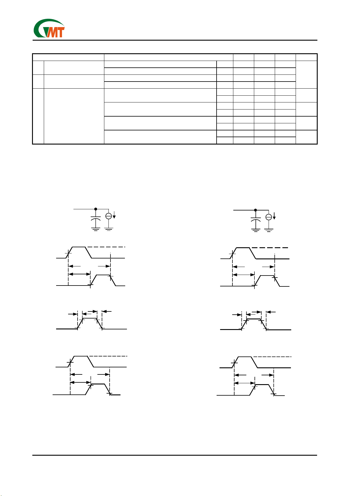
Parameter Measurement Information
LATCH
LATCH
V
V
O(xVPP)
O(xVPP)
V
V
O(xVPP)
O(xVPP)
LATCH
LATCH
V
V
O(xVPP)
O(xVPP)
xVPP
xVPP
50%
50%
t
t
pd(off)
pd(off)
t
t
pd(on)
pd(on)
10%
10%
Propagation Delay (xVPP)
Propagation Delay (xVPP)
t
t
r
r
90%
90%
10%
10%
Rise/Fall Time (xVPP)
Rise/Fall Time (xVPP)
50%
50%
t
t
off
off
t
t
on
on
Turn on/off Time (xVPP)
Turn on/off Time (xVPP)
90%
90%
90%
90%
10%
10%
t
t
f
f
I
I
O(xVPP)
O(xVPP)
V
V
DD
DD
GND
GND
GND
GND
GND
GND
V
V
DD
DD
GND
GND
GND
GND
LOAD CIRCUIT
LOAD CIRCUIT
LATCH
LATCH
V
V
O(xVCC)
O(xVCC)
V
V
O(xVCC)
O(xVCC)
LATCH
LATCH
V
V
O(xVCC)
O(xVCC)
xVCC
xVCC
50%
50%
t
t
pd(off )
pd(off )
t
t
pd(on)
pd(on)
10%
10%
Propagation Delay (xVCC)
Propagation Delay (xVCC)
t
t
r
r
90%
90%
10%
10%
Rise/Fall Time (xVCC)
Rise/Fall Time (xVCC)
50%
50%
t
t
off
off
t
t
on
on
90%
90%
Turn on/off Time (xVCC)
Turn on/off Time (xVCC)
90%
90%
10%
10%
I
I
O(xCC)
O(xCC)
t
t
f
f
V
V
DD
DD
GND
GND
GND
GND
GND
GND
V
V
DD
DD
GND
GND
GND
GND
Ver: 1.0
Jan 23, 2003
VOLTAGE WAVEFORMS
VOLTAGE WAVEFORMS
Figure 1. Test Circuits and Voltage Waveforms
5
TEL: 886-3-5788833
http://www.gmt.com.tw
Page 6

Global Mixed-mode Technology Inc.
DATA
DATA
LATCH
LATCH
CLOCK
CLOCK
D9D10
D9D10
Data Setup Time Data Hold Time Latch Delay Time
Data Setup Time Data Hold Time Latch Delay Time
D7D8
D7D8
D5
D5
D6
D6
D4 D3 D2 D1 D0
D4 D3 D2 D1 D0
G574
Clock Delay Time
Clock Delay Time
Note: Data is clocked in on the positive edge of the clock. The positive edge of the latch signal should occur
before the next positive edge of the clock. For definition of D0 to D10, see the control logic table.
Figure 2. Serial-Interface Timing for Independent xVPP Switching When MODE=5V or 3.3V
D7D8
DATA
DATA
LATCH
LATCH
Data Setup Time
Data Setup Time
D7D8
D6
D6
D5
D5
D4 D3 D2 D1 D0
D4 D3 D2 D1 D0
Data Hold Time Latch Delay Time
Data Hold Time Latch Delay Time
Clock Delay Time
Clock Delay Time
CLOCK
CLOCK
Note: Data is clocked in on the positive edge of the clock. The positive edge of the latch signal should occur
before the next positive edge of the clock. For definition of D0 to D8, see the control logic table.
Figure 3. Serial-Interface Timing When MODE = 0V or Floating
Ver: 1.0
Jan 23, 2003
6
TEL: 886-3-5788833
http://www.gmt.com.tw
Page 7

Global Mixed-mode Technology Inc.
Switching Characteristics
G574
Switching Characteristics
Ver: 1.0
Jan 23, 2003
7
TEL: 886-3-5788833
http://www.gmt.com.tw
Page 8

Global Mixed-mode Technology Inc.
G574
Switching Characteristics
Ver: 1.0
Jan 23, 2003
8
TEL: 886-3-5788833
http://www.gmt.com.tw
Page 9

Global Mixed-mode Technology Inc.
Application Information
Overview
PC Cards were initially introduced as a means to add
EEPROM (flash memory) to portable computers with
limited on-board memory. The idea of add-in cards
quickly took hold; modems, wireless LANs, Global
Positioning Satellite (GPS), multimedia, and hard-disk
versions were soon available. As the number of PC
Card applications grew, the engineering community
quickly recognized the need for a standard to ensure
compatibility across platforms. To this end, the
PCMCIA was established, comprised of members
from leading computer, software, PC Card, and semiconductor manufactures. One key goal was to realize
the “plug-and play” concept. Cards and hosts from
different vendors should be compatible—able to
communicate with one another transparently.
PC Card Power Specification
System compatibility also means power compatibility.
The most current set of specifications (PC Card Standard) set forth by the PCMCIA committee states that
power is to be transferred between the host and the
card through eight of the 68 terminals of the PC Card
connector. This power interface consists of two V
two V
ground terminals minimize connector-terminal and line
resistance. The two V
specified as separate signals but are commonly tied
together in the host to form a single node to minimize
voltage losses. Card primary power is supplied
through the V
and erase voltage is supplied through the V
nals.
Overcurrent and Over-Temperature Protection
PC Cards are inherently subject to damage that can
result from mishandling. Host systems require protection against short-circuited cards that could lead to
power supply or PCB-trace damage. Even systems
robust enough to withstand a short circuit would still
undergo rapid battery discharge into the damaged PC
Card, resulting in the rather sudden and unacceptable
loss of system power. Most hosts include fuses for
protection. However, the reliability of fused systems is
poor, as blown fuses require troubleshooting and repair, usually by the manufacturer.
The G574 takes a two-pronged approach to overcurrent protection. First, instead of fuses, sense FETs
monitor each of the power outputs. Excessive current
generates an error signal that linearly limits the output
current, preventing host damage or failure. Sense
FETs, unlike sense resistors or polyfuses, have an
added advantage in that they do not add to the series
, and four ground terminals. Multiple VCC and
PP
PP
terminals; flash-memory programming
CC
,
CC
terminals were originally
termi-
PP
G574
resistance of the switch and thus produce no additional voltage losses. Second, when an overcurrent
condition is detected, the G574 asserts a signal at
OC that can be monitored by the microprocessor to
initiate diagnostics and/or send the user a warning
message. In the event that an overcurrent condition
persists, causing the IC to exceed its maximum junction temperature, thermal-protection circuitry activates,
shutting down all power outputs until the device cools
to within a safe operating region.
12V Supply Not Required
Most PC Card switches use the externally supplied
12V V
power for switch-gate drive and other chip
PP
functions, which requires that power be present at all
times. The G574 offers considerable power savings by
using an internal charge pump to generate the required higher voltages from 5V or 3.3V input; therefore,
the external 12V supply can be disable except when
needed for flash-memory functions, thereby extending
battery lifetime. Do not ground the 12V input if the 12V
input is not used. Additional power savings are realized by the G574 during a software shutdown in which
quiescent current drops to a typical of 2µA.
3.3V Low Voltage Mode
The G574 operates in 3.3V low voltage mode when
3.3V is the only available input voltage (V
V
=0).This allows host and PC Cards to be oper-
I(12V)
I(5V)
=0,
ated in low power 3.3V only modes such as sleep
modes or pager modes. Note that in this operation
mode, the G574 derives its bias current from the 3.3V
input pin and only 3.3V can be delivered to the Card.
The 3.3V switch resistance increases, but the added
switch resistance should not be critical, because only
a small amount of current is delivered in this mode.
Voltage Transitioning Requirement
PC Cards, like portables, are migrating from 5V to
3.3V to minimize power consumption, optimize board
space, and increase logic speeds. The G574 is designed to meet all combinations of power delivery as
currently defined in the PCMCIA standard. The latest
protocol accommodates mixed 3.3V/5V systems by
first powering the card with 5V, then polling it to determine its 3.3V compatibility. The PCMCIA specification requires that the capacitors on 3.3V compatible
cards be discharged to below 0.8 V before applying
3.3V power. This ensures that sensitive 3.3V circuitry
is not subjected to any residual 5V charge and functions as a power reset. The G574 offer a selectable
V
and VPP ground state, in accordance with PCMCIA
CC
3.3V/5V switching specifications, to fully discharge the
card capacitors while switching between V
voltage.
CC
Ver: 1.0
Jan 23, 2003
9
TEL: 886-3-5788833
http://www.gmt.com.tw
Page 10

Global Mixed-mode Technology Inc.
Shutdown Mode
In the shutdown mode, which can be controlled by bit
D8 of the input serial DATA word, each of he xVCC
and xVPP outputs is forced to a high-inpedance state.
In this mode, the chip quiescent current is limited to
2µA or less to conserve battery power.
Standby Mode
The G574 can be put in standby mode by pulling
low to conserve power during low-power opera-
STBY
tion. In this mode, all of the power outputs (xVCC and
xVPP) will have a nominal current limit of 50mA.
has an internal 150 kΩ pullup resistor. The out-
STBY
put-switch status of the device must be set, allowing
the output capacitors to charge, prior to enabling the
standby mode. Changing the setting of the output
switches with the device in standby mode may cause
an overcurrent response to be generated.
Mode
The mode pin programs the switches in either G574 or
G570 mode. An internal 150 kΩ pulldown resistor is
connected to the pin. Floating or pulling the mode pin
low sets the switches in G570 mode; pulling the mode
pin high sets the switches in G574 mode. In
G570mode, xVPP outputs are dependent on xVCC
outputs. In G574 mode, xVPP is programmed independent of xVCC. Refer to G574 control-logic tables
for more information.
Output Ground Switches
Several PCMCIA power distribution switches on the
market do not have an active grounding FET switch.
These devices do not meet the PC Card specification
requiring a discharge of V
resistance can not be relied on to provide a discharge
path for voltages stored on PC Card capacitance because of possible high impedance isolation by power
management schemes. A method commonly shown to
alleviate this problem is to add to the switch output an
external 100kΩ resistor in parallel with the PC Card.
Considering that this is the only discharge path to
ground, a timing analysis show that the RC time constant delays the required discharge time to more than
2 seconds. The only way to ensure timing compatibility
with PC Card standards is to use a power-distribution
switch that has an internal ground switch, like that of
the G574, or add an external ground FET to each of
the output lines with the control logic necessary to select it.
In summary, the G574 is a complete single-chip
dual-slot PC Card power interface. It meets all currently defined PCMCIA specifications for power delivery in 5V, 3.3V, and mixed systems, and offers a serial
control interface. The G574 offers functionality, power
savings, overcurrent and thermal protection, and fault
reporting in one 30 pin SSOP surface-mount package
for maximum value added to new portable designs.
within 100ms. PC Card
CC
G574
Power Supply Considerations
The G574 has multiple pins for each of its 3.3V, 5V,
and 12V power inputs and for switched V
outputs.
CC
Any individual pin can conduct the rated input or output current. Unless all pins are connected in parallel,
the series resistance is significantly higher than that
specified, resulting in increased voltage drops and lost
power. Both 12V inputs must be connected for proper
V
switching; it is recommended that all input and
PP
output power pins be paralleled for optimum operation.
Although the G574 is fairly immune to power input
fluctuations and noise, it is generally considered good
design practice to bypass power supplies typically with
a 1µF electrolytic or tantalum capacitor paralleled by a
0.047µF to 0.1µF ceramic capacitor. It is strongly recommended that the switched V
and VPP outputs be
CC
bypassed with a 0.1µF or larger capacitor; doing so
improves the immunity of the G574 to electrostatic
discharge (ESD). Care should be taken to minimize
the inductance of PCB traces between the G574 and
the load. High switching currents can produce large
negative-voltage transients, which forward biases
substrate diodes, resulting in unpredictable performance. Similarly, no pin should be taken below –0.3V.
RESET or
RESET Inputs
To ensure that cards are in a known state after power
brownouts or system initialization, the PC Cards
should be reset at the same time as the host by applying a low impedance to the xV
and xVPP terminals
CC
to ground. A low impedance output state allows discharging of residual voltage remaining on PC Card
filter capacitance, permitting the system (host and PC
Cards) to be powered up concurrently. The RESET or
RESET input will closes internal switches S1, S4, S7,
and S11 with all other switches left open (see G574
control logic table). The G574 remains in the low impedance output state until the signal is deasserted and
further data is clocked in and latched. RESET or
RESET are provided for direct compatibility with systems that use either an active-low or active-high reset
voltage supervisor. The unused pin is internally pulled
up or down and should be left unconnected.
Overcurrent and Thermal Protection
The G574 uses sense FETs to check for overcurrent
conditions in each of the V
and V
CC
outputs. Unlike
PP
sense resistors or polyfuses, these FETs do not add to
the series resistance of the switch; therefore, voltage
and power losses are reduced. Overcurrent sensing is
applied to each output separately. When an overcurrent condition is detected, only the power output affected is limited; all other power outputs continue to
function normally. The OC indicator, normally a logic
high, is a logic low when any overcurrent condition is
detected, providing for initiation of system diagnostics
and/or sending a warning message to the user.
Ver: 1.0
Jan 23, 2003
10
TEL: 886-3-5788833
http://www.gmt.com.tw
Page 11

Global Mixed-mode Technology Inc.
During power up, the G574 controls the rise time of
the V
faulty card or connector. If a short circuit is applied
after power is established (e.g., hot insertion of a bad
card), current is initially limited only by the impedance
between the short and the power supply. In extreme
cases, as much as 10A to 15A may flow into the short
before the current limiting of the G574 engages. If the
V
may latch nondestructively in an off state. Cycling
power will reestablish normal operation.
Overcurrent limiting for the V
activate, if powered up, into a short in the range of
0.8A to 2.2A. The V
450mA. The protection circuitry acts by linearly limiting
the current passing through the switch rather than initiating a full shutdown of the supply. Shutdown occurs
only during thermal limiting.
Thermal limiting prevents destruction of the IC from
overheating if the package power-dissipation ratings are
exceeded. Thermal limiting disables all power outputs
(both A and B slots) until the device has cooled.
Functional Block Diagram
and VPP outputs and limits the current into a
CC
CC
or V
outputs are driven below ground, the G574
PP
outputs is designed to
CC
outputs limit from 120mA to
PP
G574
Logic Input and Outputs
The serial interface consists of DATA, CLOCK, and
LATCH leads. The data is clocked in on the positive
leading edge of the clock (see Figure 2 and 3 ). The bit
(D0 through D10 serial data word is loaded during the
positive edge of the latch signal. The latch signal
should occur before the next positive leading edge of
the block.
The shutdown bit of the data word places all V
V
outputs in a high-impedance state and reduces
PP
CC
and
chip quiescent current to 2µA to conserve battery
power.
The G574 serial interface is designed to be compatible
with serial-interface PCMCIA controllers and current
PCMCIA and Japan Electronic Industry Development
Association (JEIDA) standards.
An overcurrent output (
overcurrent condition in any of the V
OC ) is provided to indicate an
or VPP outputs
CC
as previously discussed.
3.3V
3.3V
3.3V
3.3V
3.3V
3.3V
12V
12V
12V
12V
5V
5V
5V
5V
5V
5V
15
15
16
16
17
17
30
30
24
24
29
29
19
19
14
14
18
18
1
1
2
2
7
7
3
3
4
4
5
5
6
6
G574
G574
S1
S1
S2
S2
S3
S3
S5
S5
S4
S4
S6
S6
CS
CS
CS
CS
CS
CS
CS
CS
Internal
Internal
Current Monitor
Current Monitor
MODE
MODE
STBY
STBY
DATA
DATA
CLOCK
CLOCK
LATCH
LATCH
RESET
RESET
RESET
RESET
OC
OC
CS
CS
CS
CSCS
CS
CSCS
CS
CS
CS
CSCS
CS
CS
GND
GND
S10
S10
S11
S11
S12
S12
S13
S13
S14
S14
S8
S9
S9
S7
S7
S8
Thermal
Thermal
9
9
AVCC
AVCC
10
10
AVCC
AVCC
11
11
AVCC
AVCC
8
8
AVPP
AVPP
20
20
BVCC
BVCC
21
21
BVCC
BVCC
22
22
BVCC
BVCC
23
23
BVPP
BVPP
12
12
Ver: 1.0
Jan 23, 2003
Both 12V pins must be connected together.
Both 12V pins must be connected together.
11
TEL: 886-3-5788833
http://www.gmt.com.tw
Page 12

Global Mixed-mode Technology Inc.
G574
G574 control logic
G574 mode (MODE pulled high)
xVPP
AVPP CONTROL SIGNALS BVPP CONTROL SIGNALS
SHDN
D8 (
1 0 0 × 0V 1 0 0 × 0V
1 0 1 0 3.3V 1 0 1 0 3.3V
1 0 1 1 5V 1 0 1 1 5V
1 1 0 × 12V 1 1 0 × 12V
1 1 1 × Hi-Z 1 1 1 × Hi-Z
0 × × × Hi-Z 0 × × × Hi-Z
D0 D1 D9
)
xVCC
AVCC CONTROL SIGNALS BVCC CONTROL SIGNALS
D8 (
)
1 0 0 0V 1 0 0 0V
1 0 1 3.3V 1 0 1 3.3V
1 1 0 5V 1 1 0 5V
1 1 1 0V 1 1 1 0V
0 × x Hi-Z 0 × x Hi-Z
SHDN
D3 D2
OUTPUT
V_AVPP
OUTPUT
V_AVCC
D8 (
D8 (
SHDN
SHDN
D4 D5 D10
)
)
D6 D7
OUTPUT
V_BVPP
OUTPUT
V-BVCC
G570 mode (MODE floating or pulled low)
xVPP
AVPP CONTROL SIGNALS BVPP CONTROL SIGNALS
D8 (
)
1 0 0 0V 1 0 0 0V
1 0 1 V_AVCC 1 0 1 V_BVCC
1 1 0 12V 1 1 0 12V
1 1 1 Hi-Z 1 1 1 Hi-Z
0 × x Hi-Z 0 × x Hi-Z
SHDN
D0 D1
OUTPUT
V_AVPP
D8 (
SHDN
OUTPUT
)
D4 D7
V-BVPP
xVCC
AVCC CONTROL SIGNALS BVCC CONTROL SIGNALS
D8 (
)
1 0 0 0V 1 0 0 0V
1 0 1 3.3V 1 0 1 3.3V
1 1 0 5V 1 1 0 5V
1 1 1 0V 1 1 1 0V
0 × x Hi-Z 0 × x Hi-Z
SHDN
D3 D2
OUTPUT
V_AVPP
D8 (
SHDN
OUTPUT
)
D6 D7
V-BVPP
Ver: 1.0
Jan 23, 2003
12
TEL: 886-3-5788833
http://www.gmt.com.tw
Page 13

Global Mixed-mode Technology Inc.
ESD Protection
The xVCC and xVPP outputs can be exposed to potentially higher discharges from the external environment
AVCC
AVCC
AVCC
GND
GND
AVCC
AVCC
AVCC
BVCC
BVCC
BVCC
BVCC
BVCC
BVCC
AVPP
AVPP
BVPP
BVPP
DATA
DATA
CLOCK
CLOCK
LATCH
LATCH
RESET
RESET
RESET
RESET
OC
OC
12V
12V
5V
5V
(Ceramic)
(Ceramic)
3.3V
3.3V
(Ceramic)
(Ceramic)
(Ceramic)
(Ceramic)
0.1µF
0.1µF
0.1µF
0.1µF
0.1µF
0.1µF
10µF
10µF
33µF
33µF
33µF
33µF
12V
12V
12V
12V
5V
5V
5V
5V
5V
5V
3.3V
3.3V
3.3V
3.3V
3.3V
3.3V
MODE
MODE
STBY
STBY
G574
G574
G574
through the PC Card connector. Bypassing the outputs
with 0.1µF capacitors protects the devices from discharges up to 10 kV.
V
V
CC
0.1µF
0.1µF
0.1µF
0.1µF
0.1µF
0.1µF
0.1µF
0.1µF
System Voltage
System Voltage
Supervisor
Supervisor
or
or
PCI Bus Reset
PCI Bus Reset
CC
V
V
CC
CC
V
V
PP1
PP1
V
V
PP2
PP2
V
V
CC
CC
V
V
CC
CC
V
V
PP1
PP1
V
V
PP2
PP2
DATA
DATA
CLOCK
CLOCK
LATCH
LATCH
GPI/O
GPI/O
PC Card
PC Card
Connector A
Connector A
PC Card
PC Card
Connector B
Connector B
PCMCIA
PCMCIA
Controller
Controller
Ver: 1.0
Jan 23, 2003
Figure 3. Detailed Interconnections and Capacitor Recommendations
13
TEL: 886-3-5788833
http://www.gmt.com.tw
Page 14

Global Mixed-mode Technology Inc.
G574
G574 30Pin Package
4°
c
L1
L
θ
7º
D
E
A1
A2
E1
A
1.15
3.6
e
b
Note:
1. Dimensional tolerance ±0.10mm
2. Plating thickness 5~15µm
3. Dimensions “D” does not include burrs, however dimension including protrusions or gate burrs
Shall be MAX. 0.20mm
Dimension “E1” does not include inter-lead flash or protrusion. Inter-lead flash or protrusion small not exceeds
4.
0.25 per side.
SYMBOL
A 1.80 1.90 2.00 0.071 0.075 0.079
A1 1.75 1.80 1.85 0.069 0.071 0.073
A2 0.05 0.10 0.15 0.002 0.004 .006
b 0.25 0.30 0.35 0.010 0.012 0.014
C 0.10 0.15 0.20 0.004 0.006 0.008
D 10.10 10.15 10.20 0.398 0.400 .402
E 7.50 ----- 7.90 0.295 ----- 0.311
E1 5.20 5.25 5.30 0.205 0.207 0.209
L1 0.53 0.68 0.83 0.021 0.027 0.033
L 1.10 1.20 1.30 0.043 0.047 0.051
e 0.65 BSC 0.026BSC
θ
MIN. NOM. MAX. MIN. NOM. MAX.
1° 4
DIMENSION IN MM DIMENSION IN INCH
7
°
°
1º
Taping Specification
Feed Direction
Typical SSOP Package Orientation
Typical SSOP Package Orientation
GMT Inc. d oes not assume any responsibility for use of any circuitry described, no circuit patent licenses are implied and GMT Inc. reserves the right at any time without notice to change said circuitry and specifications.
Ver: 1.0
Jan 23, 2003
Feed Direction
14
TEL: 886-3-5788833
http://www.gmt.com.tw
 Loading...