

Datasheet G547E1RD1U, G547E1TB1U, G547E2RD1U, G547E2TB1U, G547F1RD1U Datasheet (GMT) [ru]
...Page 1
Global Mixed-mode Technology
G5
47E/F/G/H/M
Power Distribution Switch
Features
90mΩ
Available with 5 Versions of Current Limits with
Operating Range:2.7V to 5.5V
1mS Typical Rise Time
Fast Overcurrent Response -3µs (TYPICAL)
Under voltage Lockout
100µA Quiescent Supply Current
1µA Maximum Shutdown Supply Current
Logic Level Enable Pin, Available with
No Reverse Current when Power Off
Deglitched Open-Drain Over-Current Flag
With Output Shutdown Pull-low Resister
SOT-23-6, SOP-8, MSOP-8 and TDFN3X3-8 Pack-
UL Approved_#E232223
Nemko IEC 60950-1 CB/CCA_scheme Certifica-
Ω High-Side MOSFET
ΩΩ
(G547E,G547F,G547G,G547H, G547M)
Foldback
Active-High or Active-Low Version
Output (OC )
ages
tion Report #67291
General Description
The G547 is an integrated power switch for
self-powered and bus-powered Universal Serial Bus
(USB) applications. G547E, G547F, G547G,G547H
and G547M are 90mΩ R
DS(ON)
.
Several Protection features include current limiting with
foldback, and thermal shutdown to prevent catastrophic
switch failure caused by increasing power dissipation
when continuous heavy loads or short circuit occurs. A
built-in charge pump is used to drive the N-channel
MOSFET that is free of parasitic body diode to eliminate any reversed current flow across the switch when
it is powered off.
OC is open-drain output report over-current or
over-temperature event and has typical 9ms deglitch
timeout period.
Applications
High-Side Power Protection Switch
USB Power Management
USB Host and Self-Powered Bubs
USB Bus-Powered Hubs
Hot Plug-In Power Supplies
Battery-Charger Circuits
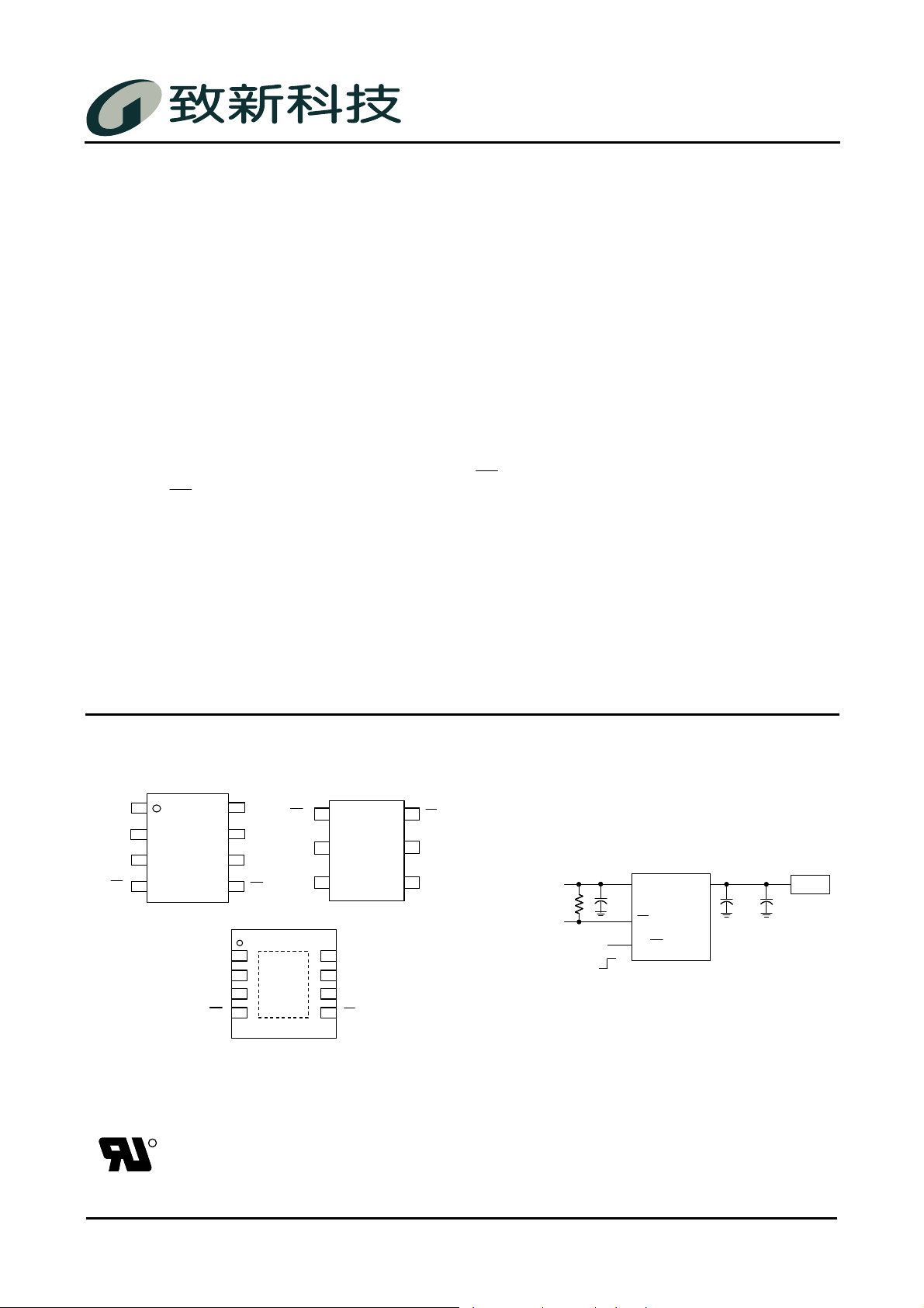
Pin Configuration Typical Application Circuit
GND
GND
IN
IN
IN
IN
EN (EN)
EN (EN)
*Pin#6 should be considered as OUT when circuit design and PCB layout, but it is NC pin actually.
*Pin#6 should be considered as OUT when circuit design and PCB layout, but it is NC pin actually.
G547
G547
1
1
2
2
3
3
4
4
SOP-8/MSOP-8
SOP-8/MSOP-8
Note: Recommend connecting the Thermal Pad
Note: Recommend connecting the Thermal Pad
OUT
OUT
8
8
EN (EN)
EN (EN)
1
1
OUT
OUT
7
7
6
6
5
5
1
GND
1
GND
IN
IN
2
2
3
3
IN
IN
EN (EN)
EN (EN)
4
4
to the GND for excellent power dissipation.
to the GND for excellent power dissipation.
GND
GND
OUT*
OUT*
OC
OC
G547
G547
Thermal
Thermal
Pad
Pad
TDFN3X3-8
TDFN3X3-8
2
2
IN
IN
8
8
7
7
6
6
5
5
G547
G547
SOT-23-6
SOT-23-6
OUT
OUT
OUT
OUT
OUT*
OUT*
OC
OC
6
6
OC
OC
5 OUT
5 OUT
OUT
OUT
43
43
G547
*
*
IN
IN
OC
OC
EN(EN)
EN(EN)
G547
OUT
OUT
Power Supply
Power Supply
2.7V to 5.5V
2.7V to 5.5V
1µF
1µF
ON
ON
OFF
OFF
*: 1µF of input capacitor is enough in most application cases.
*: 1µF of input capacitor is enough in most application cases.
If the PCB trace of power rail to IN is long, larger input capacitor is necessary.
If the PCB trace of power rail to IN is long, larger input capacitor is necessary.
R
R
0.1µF
0.1µF
22µF
22µF
Load
Load
UL Recognized Component
UL Recognized Component
Ver:1.5
Sep 08, 2011
1
Page 2
Global Mixed-mode Technology
Ordering Information
547E/F/G/H/M
G
ORDER
NUMBER
G547E1TB1U 57EAx Active High 2.5A 90mΩ Yes -40°C to +85°C SOT-23-6
G547E2TB1U 57EBx Active Low 2.5A 90mΩ Yes -40°C to +85°C SOT-23-6
G547F1TB1U 57FAx Active High 2A 90mΩ Yes -40°C to +85°C SOT-23-6
G547F2TB1U 57FBx Active Low 2A 90mΩ Yes -40°C to +85°C SOT-23-6
G547G1TB1U 57GAx Active High 1.5A 90mΩ Yes -40°C to +85°C SOT-23-6
G547G2TB1U 57GBx Active Low 1.5A 90mΩ Yes -40°C to +85°C SOT-23-6
G547H1TB1U 57HAx Active High 1A 90mΩ Yes -40°C to +85°C SOT-23-6
G547H2TB1U 57HBx Active Low 1A 90mΩ Yes -40°C to +85°C SOT-23-6
G547M1TB1U 57MAx Active High 3.7A 90mΩ Yes -40°C to +85°C SOT-23-6
G547M2TB1U 57MBx Active Low 3.7A 90mΩ Yes -40°C to +85°C SOT-23-6
G547E1P11U G547E1 Active High 2.5A 90mΩ Yes -40°C to +85°C SOP-8
G547E2P11U G547E2 Active Low 2.5A 90mΩ Yes -40°C to +85°C SOP-8
G547F1P11U G547F1 Active High 2A 90mΩ Yes -40°C to +85°C SOP-8
G547F2P11U G547F2 Active Low 2A 90mΩ Yes -40°C to +85°C SOP-8
G547G1P11U G547G1 Active High 1.5A 90mΩ Yes -40°C to +85°C SOP-8
G547G2P11U G547G2 Active Low 1.5A 90mΩ Yes -40°C to +85°C SOP-8
G547H1P11U G547H1 Active High 1A 90mΩ Yes -40°C to +85°C SOP-8
G547H2P11U G547H2 Active Low 1A 90mΩ Yes -40°C to +85°C SOP-8
G547M1P11U G547M1 Active High 3.7A 90mΩ Yes -40°C to +85°C SOP-8
G547M2P11U G547M2 Active Low 3.7A 90mΩ Yes -40°C to +85°C SOP-8
G547E1P81U G547E1 Active High 2.5A 90mΩ Yes -40°C to +85°C MSOP-8
G547E2P81U G547E2 Active Low 2.5A 90mΩ Yes -40°C to +85°C MSOP-8
G547F1P81U G547F1 Active High 2A 90mΩ Yes -40°C to +85°C MSOP-8
G547F2P81U G547F2 Active Low 2A 90mΩ Yes -40°C to +85°C MSOP-8
G547G1P81U G547G1 Active High 1.5A 90mΩ Yes -40°C to +85°C MSOP-8
G547G2P81U G547G2 Active Low 1.5A 90mΩ Yes -40°C to +85°C MSOP-8
G547H1P81U G547H1 Active High 1A 90mΩ Yes -40°C to +85°C MSOP-8
G547H2P81U G547H2 Active Low 1A 90mΩ Yes -40°C to +85°C MSOP-8
G547M1P81U G547M1 Active High 3.7A 90mΩ Yes -40°C to +85°C MSOP-8
G547M2P81U G547M2 Active Low 3.7A 90mΩ Yes -40°C to +85°C MSOP-8
G547E1RD1U 547E1 Active High 2.5A 90mΩ Yes -40°C to +85°C TDFN3X3-8
G547E2RD1U 547E2 Active Low 2.5A 90mΩ Yes -40°C to +85°C TDFN3X3-8
G547F1RD1U 547F1 Active High 2A 90mΩ Yes -40°C to +85°C TDFN3X3-8
G547F2RD1U 547F2 Active Low 2A 90mΩ Yes -40°C to +85°C TDFN3X3-8
G547G1RD1U 547G1 Active High 1.5A 90mΩ Yes -40°C to +85°C TDFN3X3-8
G547G2RD1U 547G2 Active Low 1.5A 90mΩ Yes -40°C to +85°C TDFN3X3-8
G547H1RD1U 547H1 Active High 1A 90mΩ Yes -40°C to +85°C TDFN3X3-8
G547H2RD1U 547H2 Active Low 1A 90mΩ Yes -40°C to +85°C TDFN3X3-8
G547M1RD1U 547M1 Active High 3.7A 90mΩ Yes -40°C to +85°C TDFN3X3-8
G547M2RD1U 547M2 Active Low 3.7A 90mΩ Yes -40°C to +85°C TDFN3X3-8
Note: TB: SOT-23-6 P1: SOP-8 P8: MSOP-8 RD: TDFN3X3-8
1: Bonding Code
U: Tape & Reel
MARKING ENABLE
Current
Limit
Output
MOS
R
DS(ON)
Output
Shutdown
Resistor
TEMP.
RANGE
PACKAGE
(Green)
Ver:1.5
Sep 08, 2011
2
Page 3
Global Mixed-mode Technology
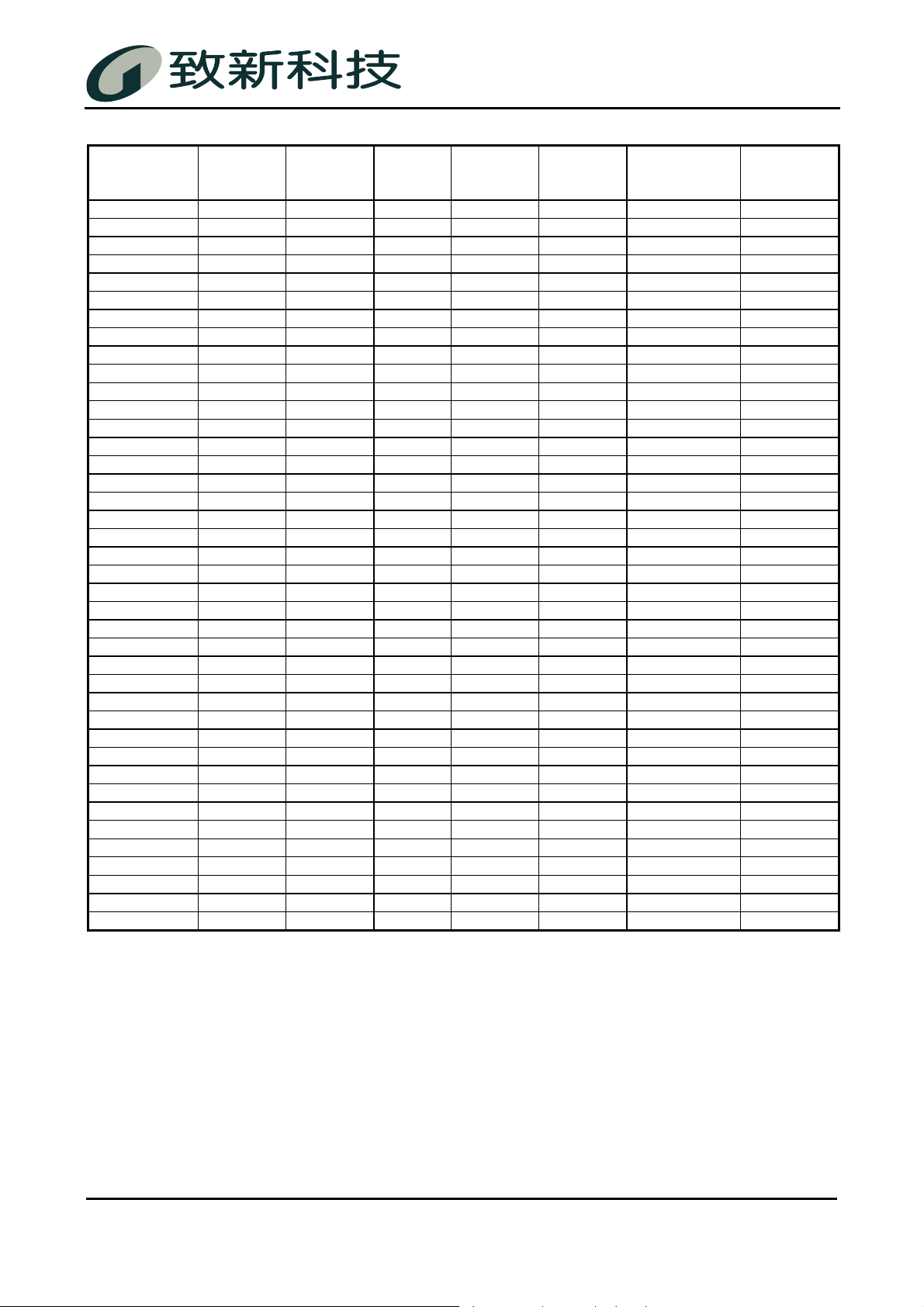
Absolute Maximum Ratings
Supply Voltage (VIN) . . . . . . . . . . . . . . . . . . . . . . . . .6V
Output Voltage (V
Output Current (I
Enable Input (VEN) . . . . . . . . . . . . . . . . . . . .-0.3V to 6V
Thermal Resistance Junction to Ambient, (θJA)*
SOT-23-6. . . . . . . . . . . . . . . . . . . . . . . . . . . . 250°C/W
SOP-8 . . . . . . . . . . . . . . . . . . . . . . . . . . . . . .160°C/W
MSOP-8 . . . . . . . . . . . . . . . . . . . . . . . . . . . . .180°C/W
TDFN3X3-8 . . . . . . . . . . . . . . . . . . . . . . . . . . .170°C/W
Continuous Power Dissipation (TA = +25°C)*
SOT-23-6 . . . . . . . . . . . . . . . . . . . . . . . . . . . . . . 0.5W
*Please refer to Minimum Footprint PCB Layout Section.
) . . . . . . . . . . . . . . . . . . . . . . . 6V
OUT
) . . . . . . . . . . . . . Internally Limited
OUT
SOP-8 . . . . . . . . . . . . . . . . . . . . . . . . . . . . . . . . .0.71W
MSOP-8 . . . . . . . . . . . . . . . . . . . . . . . . . . . . . . .0.64W
TDFN3X3-8 . . . . . . . . . . . . . . . . . . . . . . . . . . . . 0.67W
Junction Temperature . . . . . . . . . . . . . . . .. . . . . 150°C
Storage Temperature (TS) . . . . . . . . . . .-65°C to +150°C
Reflow Temperature (soldering, 10sec) . . . . . . . 260°C
ESD Protection . . . . . . . . . . . . . . . . . . . . . . . . . . . . 2kV
Operating Ratings
Supply Voltage (VIN) . . . . . . . . . . . . . . . . . . . 3V to 5.5V
Operating Temperature (TA) . . . . . . . . -40°C to +85°C
547E/F/G/H/M
G
Electrical Characteristics
VIN = 5V, CIN=1µF, C
The device is not guaranteed to function outside its operating conditions. Parameters with MIN and/or MAX limits are 100%
tested at +25°C, unless otherwise specified.
PARAMETER CONDITION MIN TYP MAX UNITS
Input Voltage Rage
Output MOS R
Supply Current --- 100 135 µA
Output Turn-on Rising Time RL=10Ω, 90% Settling 0.4 1 1.5 ms
Current Limit Threshold
Short-circuit Current
EN Input Threshold-High VIH 1.4 1.6 1.8 V
EN Input Threshold-Low VIL 0.8 1.3 1.6 V
Shutdown Supply Current --- 0.1 1 µA
Shutdown Pull Low Resistance --- 75 150 Ω
Output Leakage Current EN=”0”, V
VIN Under Voltage Lockout 2.2 2.5 2.7 V
VIN Under Voltage Hysteresis --- 200 --- mV
Thermal Limit --- 135 --- °C
Thermal Limit Hysteresis --- 20 --- °C
OCDeglitch OCassertion or deassertion
OCOutput Low Voltage
OCOff-State Current
tS Response Time to Short Circuit VIN=5V, see figure 1. --- 3 --- µs
DS(ON)
=1µF, RL=10ΩΩΩΩ TA = 25°C.
OUT
G547E1/G547E2, I
G547F1/G547F2, I
G547G1/G547G2, I
G547H1/G547H2, I
G547M1/G547M2, I
G547E1/G547E2,V
G547F1/G547F2,V
G547G1/G547G2,V
G547H1/G547H2,V
G547M1/G547M2,V
G547E1/G547E2,V
G547F1/G547F2,V
G547G1/G547G2,V
G547H1/G547H2, V
G547M1/G547M2, V
IOC= 2mA
VOC= 5V --- --- 1
2.7 --- 5.5 V
=2A
OUT
=1.5A
OUT
=1A
OUT
=0.5A
OUT
=2.5A
OUT
=4V 2.01 2.5 3
OUT
=4V 1.6 2 2.7
OUT
=4V 1.1 1.5 2
OUT
=4V 0.6 1 1.45
OUT
=4V 2.8 3.7 5
OUT
=0V, 2.7V<VIN<5.5V 0.2 1.7 2.6
OUT
=0V, 2.7V<VIN<5.5V 0.2 1.3 2
OUT
=0V, 2.7V<VIN<5.5V 0.2 1 1.6
OUT
=0V, 2.7V<VIN<5.5V 0.2 0.7 1.2
OUT
=0V, 2.7V<VIN<5.5V 0.2 2 3.5
OUT
=0V --- 0.5 1 µA
OUT
I
I
SC
SC
--- 90 110 mΩ
4 9 15 ms
--- --- 0.4 V
A
A
µA
I
I
OUT
OUT
t
t
S
S
F
F
igure 1
igure 1
Ver:1.5
Sep 08, 2011
3
Page 4
Global Mixed-mode Technology
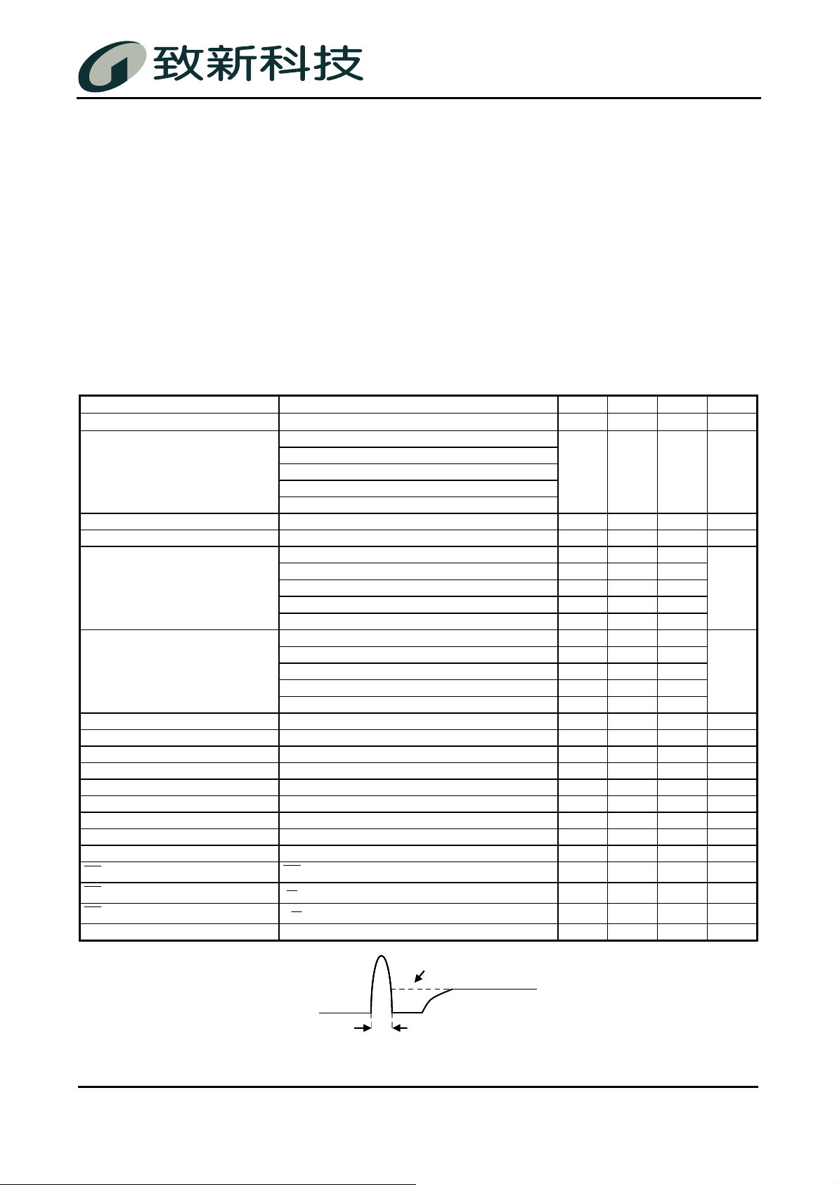
Typical Performance Characteristics
(VIN= 5V, CIN=1µF, C
A)
µ
(
Q
Supply Current I
Supply Current vs. Input Voltage
120
TA=85°C
100
80
60
40
20
VEN=0V
0
2.5 3.0 3.5 4.0 4.5 5.0 5.5
=1µF, VEN=0V, TA=25°C, test by G547F1, unless otherwise noted.)
OUT
TA=25°C
Input Voltage VIN (V)
TA=-45°C
547E/F/G/H/M
G
Shutdown Supply Current vs. Input Voltage
1
0.8
0.6
A)
µ
0.4
0.2
0
-0.2
-0.4
-0.6
Shutdown Supply Current (
-0.8
-1
2.5 3.0 3.5 4.0 4.5 5.0 5.5
VEN=5V
TA=25°C
TA=-45°C
Input Voltage VIN (V)
TA=85°C
Enable Input Threshold vs. Input Voltage
2.0
1.8
1.6
1.4
V
EN
Falling
VEN Rising
1.2
Enable Input Threshold (V)
1.0
0.8
3.0 3.5 4.0 4.5 5.0 5.5
Input Voltage VIN (V)
OC Deglitch Time vs. Input Voltage
14
OC deassertion
13
12
OC assertion
11
OC Deglitch Time (ms)
10
9
2.5 3 3.5 4 4.5 5 5.5
I
nput Voltage VIN (V)
Enable Input Threshold vs. Temperature
2.0
1.8
VEN Falling
1.6
1.4
Enable Input Threshold (V)
1.2
VEN Rising
VIN=5V
1.0
-45 -35 -25 -15 -5 5 15 25 35 45 55 65 75 85
Ambient Temperature (°C)
UVLO Threshold vs. Temperature
3.2
3.0
2.8
2.6
2.4
2.2
2.0
1.8
UVLO Threshold (V)
1.6
1.4
1.2
1.0
-45 -35 -25 -15 -5 5 15 25 35 45 55 65 75 85
A
VIN Rising
V
Falling
IN
mbient Temperature (°C)
Ver:1.5
S
ep 08, 2011
4
Page 5
Global Mixed-mode Technology
Typical Performance Characteristics (continued)
200
180
160
140
(mΩ)
120
DS (ON)
100
On-Resistancr R
ON-Resistance vs. Input Voltage ON-Resistance vs. Temperature
I
=1A
OUT
TA=25°C
80
60
40
20
0
3.0 3.5 4.0 4.5 5.0 5.5
Input Voltage VIN (V)
TA=85°C
TA=-45°C
547E/F/G/H/M
G
140
I
=1A
OUT
120
VIN=3V
100
(mΩ)
80
DS (on)
60
40
On-Resistance R
20
0
-45 -35 -25 -15 -5 5 15 25 35 45 55 65 75 85
VIN=3.5V
Temperature (°C)
VIN=5V
Current Limit Threshold vs. Input Voltage
2.7
TA=-45°C
2.4
2.1
1.8
1.5
Current Limit Threshod ILIMT (A)
V
OUT=VIN
1.2
2.5 3.0 3.5 4.0 4.5 5.0 5.5
TA=25°C
- 1
Input Voltage VIN (V)
TA=85°C
Overcurrent Protection Characteristics
5.1
4.8
4.5
4.2
3.9
3.6
3.3
3.0
2.7
2.4
2.1
1.8
Output Voltage (V)
1.5
1.2
0.9
0.6
VIN=5V
0.3
0.0
0 0.2 0.4 0.6 0.8 1 1.2 1.4 1.6 1.8 2 2.2 2.4 2.6
Output Current (A)
TA=85°C
TA=25°C
TA=-45°C
Short Circuit Current vs. Input Voltage
2.1
1.8
1.5
1.2
TA=25°C
0.9
0.6
Short Circuit Current IOS (A)
0.3
V
=0V
OUT
0
2.5 3.0 3.5 4.0 4.5 5.0 5.5
TA=-45°C
TA=85°C
Input Voltage VIN (V)
Overcurrent Protection Characteristics
2.7
2.4
2.1
1.8
1.5
1.2
0.9
Output Voltage (V)
0.6
VIN=2.7V
0.3
0.0
0 0.2 0.4 0.6 0.8 1 1.2 1.4 1.6 1.8 2 2.2 2.4
TA=85°C
TA=25°C
TA=-45°C
Output Current (A)
Ver:1.5
S
ep 08, 2011
5
Page 6

Global Mixed-mode Technology
Typical Performance Characteristics (continued)
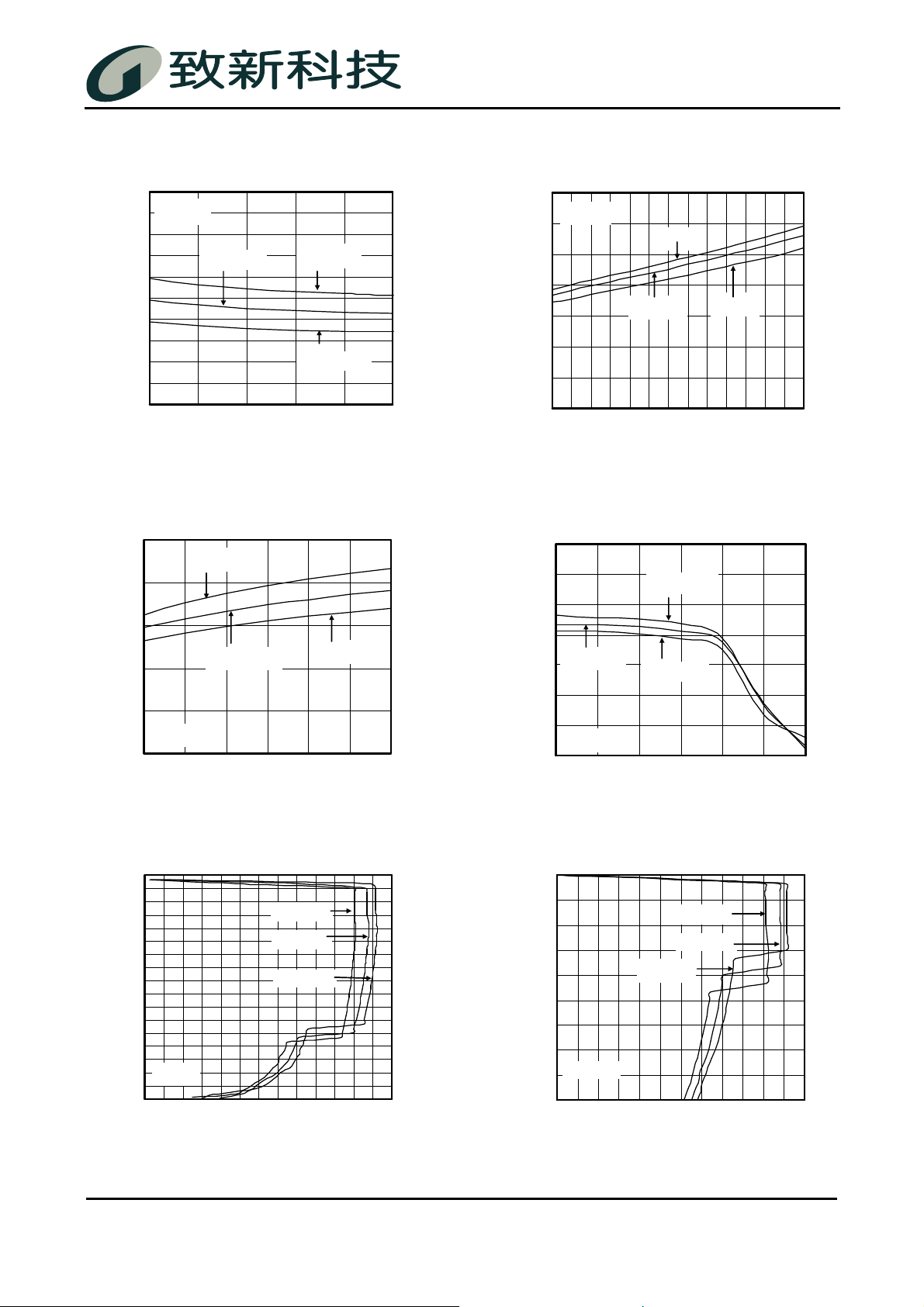
Turn on Delay Time and Rise Time Turn off Delay Time and Fall Time
547E/F/G/H/M
G
Inrush Current With Different Load Capacitance Thermal Shutdown Response
UVLO Protection at Rising
UVLO Protection at Falling
Ver:1.5
S
ep 08, 2011
6
Page 7

Global Mixed-mode Technology
Typical Performance Characteristics (continued)
Inrush Short Circuit Response
547E/F/G/H/M
G
Short Circuit Response at Start up
Short-Circuit Current, Device Enable into Short
Capacitance Load Inrush Response Capacitance Load Inrush Response
Resistance Load Inrush Response
Ver:1.5
S
ep 08, 2011
7
Page 8

Global Mixed-mode Technology
Minimum Footprint PCB Layout Section
SOP-8 MSOP-8
SOT-23-6
SOT-23-6
SOP-8 MSOP-8
547E/F/G/H/M
G
TDFN3X3-8
TDFN3X3-8
Ver:1.5
S
ep 08, 2011
8
Page 9

Global Mixed-mode Technology
Pin Description
547E/F/G/H/M
G
PIN
SOT-23-6 SOP-8/MSOP-8 TDFN3X3-8
2 1 1 GND Ground
3 2,3 2,3 IN
1 4 4
6 5 5
4,5 6,7,8 6,7,8 OUT
Thermal Pad
NAME PIN FUNCTION
EN(EN )
OC Over-Current: Open-DrainOC output.
Block Diagram
EN
EN
(EN)
(EN)
Clock
Clock
Input Supply: Output MOSFET Drain, which also supplies IC's in-
ternal circuitry. Connect to positive supply.
Enable: Logic level enable input.
Make sure EN pin never floating.
Switch Output: Output MOSFET Source of switch. Typically connect
to switched side of load.
Recommend connecting the Thermal Pad to the GND for excellent
power dissipation.
IN
IN
Gate Control
Gate Control
GND
GND
BandGap
BandGap
Reference
Reference
UVLO
UVLO
Overcurrent
Overcurrent
Limiting
Limiting
Thermal Sense
Thermal Sense
CMP
CMP
Shutdown Signal
Shutdown Signal
OC Deglitch logic
OC Deglitch logic
Current
Current
Sense
Sense
OUT
OUT
OC
OC
Ver:1.5
S
ep 08, 2011
9
Page 10

Global Mixed-mode Technology
Functional Description
Input and Output
IN (input) is the power supply connection to the logic
circuitry and the drain of the output MOSFET. OUT
(output) is the source of the output MOSFET. In a
typical application, current flows through the switch
from IN to OUT toward the load. Both OUT pins must
be connected together to the load.
Thermal Shutdown
Thermal shutdown protects G547 from excessive
power dissipation. If the die temperature exceeds
135°C, the MOSFETS switch is shut off. 20°C of hystersis prevents the switch from turning on until the die
temperature drops to 115°C. Thermal shutdown circuit
functions only when the switch is enabled.
Undervoltage Lockout
UVLO (undervoltage lockout) prevents the output
MOSFET from turning on until IN (input voltage) exceeds 2.5V typically. After the switch turns on, if the
voltage drops below 2.3V typically, UVLO shuts off the
output MOSFET.
Current Limiting
The typical current limit value of G547 is 3.7A, 2.5A, 2A,
1.5A, 1A . There is foldback of current limit when V
1.5V (See Typical Performance Characteristics).
OUT
G547E/F/G/H/M
OC Function
The OC open-drain output is asserted (active low)
when an over current or overtemperature shutdown
condition is encountered after a 9-ms deglitch timeout.
The output remains asserted until the overcurrent or
overtemperature condition is removed.
Applications Information
Supply Filtering
A 1µF bypass capacitor from IN to GND, located
near the G547, is strongly recommended to control
supply transients. Without a bypass capacitor, an
output short may cause sufficient ringing on the input
(from supply lead inductance) to damage internal
control circuitry.
Input transients must not exceed the absolute maximum supply voltage (V
duration.
EN, the Enable Input
EN must be driven logic high or logic low for a clearly
defined input. Floating the input may cause unpredictable operation. EN should not be allowed to go
negative with respect to GND.
<
= 6V) even for a short
IN max
Ver:1.5
S
ep 08, 2011
1
0
Page 11

Global Mixed-mode Technology
Test Circuit
Timing Diagrams
Device
Device
Under
Under
Test
Test
OUT
OUT
I
I
OUT
OUT
C
C
OUT
OUT
V
V
OUT
OUT
C
R
C
R
L
L
L
L
Current Probe
Current Probe
G547E/F/G/H/M
I
I
L
L
t
t
R
R
90%
90%
V
V
OUT
OUT
50%
V
V
EN
EN
V
V
OUT
OUT
50%
t
t
ON
ON
10%
10%
Output Rise and Fall Times
Output Rise and Fall Times
90%
90%
90%
90%
t
t
OFF
OFF
10%
10%
10%
10%
t
t
F
F
Ver:1.5
S
ep 08, 2011
Switch Delay Times
Switch Delay Times
1
1
Page 12

Global Mixed-mode Technology
Package Information
547E/F/G/H/M
G
Taping Specification
SOT-23-6 Package
P
ACKAGE Q’TY/REEL
SOT-23-6 3,000 ea
Ver:1.5
S
ep 08, 2011
1
2
Page 13

Global Mixed-mode Technology
G547E/F/G/H/M
Taping Specification
SOP-8 Package
PACKAGE Q’TY/REEL
SOP-8 2,500 ea
Ver:1.5
S
ep 08, 2011
1
3
Page 14

Global Mixed-mode Technology
G547E/F/G/H/M
Taping Specification
MSOP-8 Package
PACKAGE Q’TY/REEL
MSOP-8 3,000 ea
Ver:1.5
S
ep 08, 2011
1
4
Page 15

Global Mixed-mode Technology
G547E/F/G/H/M
Taping Specification
TDFN3X3-8 Package
PACKAGE Q’TY/REEL
TDFN3X3-8 3,000 ea
GMT Inc. does not assume any responsibility for use of any circuitry described, no circuit patent licenses are implied and GMT Inc. reserves the right at any time without notice to change said circuitry and specifications.
Ver:1.5
S
ep 08, 2011
1
5
Page 16

 Loading...