

Page 1

Global Mixed-mode Technology Inc.
G218B
Ultra160 Multi-mode LVD/SE SCSI Terminator
Features
Auto-selectable multi-mode Single-Ended
or LVD Termination
Meets SCSI-1, SCSI-2, SCSI-3 SPI Ultra
(Fast-20), Ultra 2(SPI-2 LVD), Ultra160 (SPI-3
LVD) standards.
Supports active negation
3pF channel capacitance
Thermal protection
Hot-Swap compatible
5% tolerance on SE and LVD termination
resistance
28 and 36 pin SSOP package
28 Pin SSOP: Pin Compatible with DS2119
36 Pin SSOP: Pin Compatible with DS2118,
LX5241 and UCC5630
Applications
Server and workstation
High-end PC
Industrial PC
Disk Array (RAID)
SCSI cable
Pin Configuration
General Description
The G218B Multi-mode LVD/SE SCSI terminator provides a smooth transition into the next generation of
the SCSI Parallel Interface (SPI-3). It automatically
senses the bus, via DIFFSENS, and switches the termination to either single-ended (SE) or low voltage
differential (LVD) SCSI, dependent on which type of
devices are connected to the bus. If the G218B detects a HVD SCSI device, it switches to a high impedance state. For a 16-bit Wide SCSI bus to be operational, three G218B terminators are needed.
The Multi-mode terminator contains all functions required to terminate and auto detect and switch modes
for SCSI Parallel Interface (SPI) bus architectures. For
the SE termination, one regulator and nine precision
110ohm resistors are used. For the LVD termination,
the G218B integrates 18 regulated supplies with nine
precision resistor strings.
VREF
VREF
VREF
NC/HS GND
NC/HS GND
NC/HS GND
DISCNCT
DISCNCT
DISCNCT
Ver 1.3
Jul 19, 2002
R1+
R1+
R1+
R1-
R1-
R1-
R2+
R2+
R2+
R2-
R2-
R2-
R3+
R3+
R3+
R3-
R3-
R3-
R4+
R4+
R4+
R4-
R4-
R4-
R5+
R5+
R5+
R5-
R5-
R5-
GND
GND
GND
G218B
G218B
G218B
1
1
1
2
2
2
3
3
3
4
4
4
5
5
5
6
6
6
7
7
7
8
8
8
9
9
9
10
10
10
11
11
11
12
12
12
13
13
13
14
14
14
28Pin SSOP/TSSOP
28Pin SSOP/TSSOP
28Pin SSOP/TSSOP
28
28
28
27
27
27
26
26
26
25
25
25
24
24
24
23
23
23
22
22
22
21
21
21
20
20
20
19
19
19
18
18
18
17
17
17
16
16
16
15
15
15
TPWR
TPWR
TPWR
TPWR
TPWR
TPWR
R9-
R9-
R9-
R9+
R9+
R9+
R8-
R8-
R8-
R8+
R8+
R8+
NC/HS GND
NC/HS GND
NC/HS GND
R7-
R7-
R7-
R7+
R7+
R7+
R6-
R6-
R6-
R6+
R6+
R6+
DIFFB
DIFFB
DIFFB
DIFFSENSE
DIFFSENSE
DIFFSENSE
M/S
M/S
M/S
1
G218B
G218B
36
36
1
1
VREF
VREF
2
2
NC
NC
3
3
NC
NC
4
4
R1+
R1+
5
5
R1-
R1-
6
6
R2+
R2+
R2-
R2-
7
7
HS/GND
HS/GND
HS/GND
HS/GND
HS/GND
HS/GND
DISCNCT
DISCNCT
R3+
R3+
R3-
R3-
R4+
R4+
R4-
R4-
R5+
R5+
R5-
R5-
GND
GND
10
10
11
11
12
12
13
13
14
14
15
15
17
17
18
18
16
16
8
8
9
9
36Pin SSOP
36Pin SSOP
TPWR
TPWR
35
35
HVD
HVD
34
34
LVD
LVD
33
33
SE
SE
32
32
R9-
R9-
31
31
R9+
R9+
30
30
R8-
R8-
29
29
R8+
R8+
HS/GND
HS/GND
28
28
27
27
HS/GND
HS/GND
26
26
HS/GND
HS/GND
25
25
R7-
R7-
24
24
R7+
R7+
23
23
R6-
R6-
22
22
R6+
R6+
DIFFB
DIFFB
21
21
20
20
DIFFSENSE
DIFFSENSE
19
19
M/S
M/S
TEL: 886-3-5788833
http://www.gmt.com.tw
Page 2
Global Mixed-mode Technology Inc.
G218B
Ordering Information
PART NUMBER TEMP. RANGE PIN-PACKAGE FEATURE
G218BT-S4 0ºC-70ºC SSOP-28 pin / Tube DISCNCT does not disable VREF
G218BR-S4 0ºC-70ºC SSOP-28 pin / Tape & Reel DISCNCT does not disable VREF
G218BT-S5 0ºC-70ºC SSOP-36 pin / Tube DISCNCT does not disable VREF
G218BR-S5 0ºC-70ºC SSOP-36 pin / Tape & Reel DISCNCT does not disable VREF
G218BT-D3 0ºC-70ºC TSSOP-28 pin / Tube DISCNCT does not disable VREF
G218BR-D3 0ºC-70ºC TSSOP-28 pin / Tape & Reel DISCNCT does not disable VREF
Note:
DIFFSENSRefers to the SCSI bus signal.
DIFFSENSERefers to the G218B pin name and internal circuitry relating to differential sensing.
DIFFBRefers to the G218B pin name and internal circuitry relating to monitoring the DIFFSENS line.
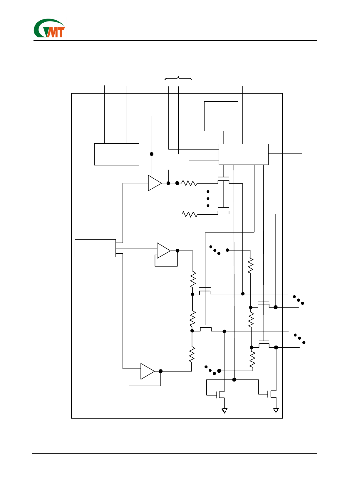
Functional Description
The G218B is used in multi-mode active termination
applications, where single ended (SE) and low voltage
differential (LVD) devices might coexist. The LVD termination section consists of 18 source/sink amplifiers
(VTOP, VBOT), biasing circuitry and nine precision
resistor strings (RTOP, RMID, RBOT). The SE termination section consists of a 2.85V source/sink regulator with 9 precision 110ohm resistor. The DIFFSENSE
section consists of a 1.3V, 5mA driver and a sensing
circuit (Figure 1)
DIFFSENS is used to identify which types of SCSI
devices are present on the bus. If the voltage on
DIFFSENS is between 0-0.5V the bus is single-ended;
if it is between 0.7-1.9V the bus is LVD; and if it is
greater than 2.4V, the bus is HVD.
The G218B DIFFB pin monitors the DIFFSENS line to
determine the proper operating mode of the device;
this mode is indicated by the SE/LVD/HVD outputs.
HVD Isolation Mode
is an HVD (high voltage differential) device on the
SCSI bus and isolates the termination pins from the
bus.
When DISCNCT is pulled high, the termination pins
are isolated from the SCSI bus, and the bus mode
indicators (SE/LVD/HVD) as well as VREF remains
active. During thermal shutdown, the termination pins
are isolated from the SCSI bus and VREF becomes
high impedance. The DIFFSENSE driver is shut down
during either of these two events.
To ensure proper operation, the TPWR pin should be
connected to the SCSI bus TERMPWR line. As with all
analog circuitry, the TERMPWR lines should be bypassed locally. A 2.2µF capacitor and a 0.01µF high
frequency capacitor is recommended between TPWR
The G218B identifies that there
and ground and placed as close as possible to the
G218B. The G218B should be placed as close as
possible to the SCSI connector to minimize signal and
power trace length, thereby resulting in less input capacitance and reflections which can degrade the bus
signals.
The DIFFSENSE pin can drive the SCSI DIFFSENS
line (when M/S is pulled high) to determine the SCSI
bus operating mode. The G218B switches to the termination mode that is appropriate for the bus based on
the value of the DIFFSENS voltage. These modes are:
LVD mode
resistor string with two amplifiers. This configuration
yields a 105Ω differential and 150Ω common mode
impedance. A fail safe bias of 112mV is maintained
when no drivers are connected to the SCSI bus.
SE mode
line turns off, the active terminator will pull that signal
line to 2.85 volts (quiescent state). When used with an
active negation driver, the power amp can sink 22mA
per line while keeping the voltage reference in regulation. The terminating resistors maintain their 110Ω
value.
To maintain the specified regulation, a 4.7µF capacitor
is required between the VREF pin and ground of each
G218B. A high frequency cap (0.1µF ceramic recommended) can also be placed on the VREF pin in applications that use fast rise/fall time drivers. A typical
SCSI bus configuration is shown in Figure2.
An internal pull down resistor assures that the G218B
will be terminating the bus if the DISCNCT pin is left
floating.
LVD termination is provided by a precision
When the external driver for a given signal
Ver 1.3
Jul 19, 2002
2
TEL: 886-3-5788833
http://www.gmt.com.tw
Page 3
Global Mixed-mode Technology Inc.
Block Diagram
VREF
VREF
(Figure 1)
M/ S
M/ S
DIFFSENSE
DIFFSENSE
CIRCUITRY
CIRCUITRY
DIFFSENSE
DIFFSENSE
(
(
36pin SSOP only
36pin SSOP only
LVD
LVD
SE
SE
VREF
VREF
HV D
HV D
110 Ohms
110 Ohms
)
)
SHUTDOWN
SHUTDOWN
DISCNCT
DISCNCT
THER MAL
THER MAL
CIRCUITRY
CIRCUITRY
CO NTROL
CO NTROL
LOGIC
LOGIC
R1-
R1-
G218B
DIFFB
DIFFB
REFERENCE
REFERENCE
GENERAT ION
GENERAT ION
R9-
R9-
110 Ohms
110 Ohms
VTOP1
VTOP1
+
+_+
_
_
RTO P9
X 9
X 9
RTO P1
RTO P1
R1-
R1-
RMI D1
RMI D1
R1+
R1+
RBO T1
RBO T1
+
+_+
_
_
VBOT1
VBOT1
RTO P9
RMI D9
RMI D9
RBO T9
RBO T9
R9-
R9-
R9+
R9+
R1-
R1-
R1+
R1+
R9-
R9-
R9+
R9+
Ver 1.3
Jul 19, 2002
X 9
X 9
3
SE
SE
GND
GND
DRIV ER
DRIV ER
TEL: 886-3-5788833
http://www.gmt.com.tw
Page 4
Global Mixed-mode Technology Inc.
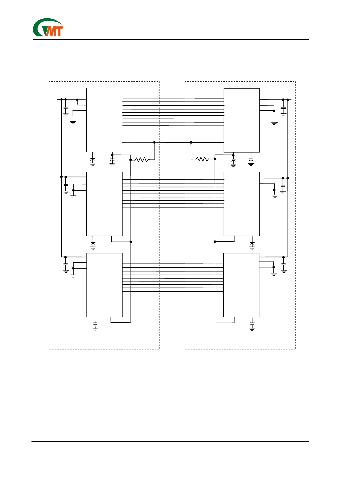
SCSI Bus Configuration
TERMPWR
TERMPWR
TERMPWR
2.2µF
2.2µF
2.2µF
2.2µF
2.2µF
2.2µF
TPWR
TPWR
TPWR
M/S
M/S
M/S
DISCNCT
DISCNCT
DISCNCT
VREF DIFFB
VREF DIFFB
VREF DIFFB
4.7µF
4.7µF
4.7µF
TPWR
TPWR
TPWR
M/S
M/S
M/S
DISCNCT
DISCNCT
DISCNCT
G218B
G218B
G218B
DIFFSENSE
DIFFSENSE
DIFFSENSE
(Figure 2)
0.1µF
0.1µF
0.1µF
20K
20K
20K
G218B
CONTROL LINES (9)
CONTROL LINES (9)
CONTROL LINES (9)
DIFFSENS
DIFFSENS
DIFFSENS
DATA LINES (9)
DATA LINES (9)
DATA LINES (9)
20K
20K
20K
G218B
G218B
G218B
DIFFSENSE
DIFFSENSE
DIFFSENSE
DIFFB VREF
DIFFB VREF
DIFFB VREF
0.1µF
0.1µF
0.1µF
TPWR
TPWR
TPWR
M/S
M/S
M/S
DISCNCT
DISCNCT
DISCNCT
TPWR
TPWR
TPWR
M/S
M/S
M/S
DISCNCT
DISCNCT
DISCNCT
4.7µF
4.7µF
4.7µF
TERMPWR
TERMPWR
TERMPWR
2.2µF
2.2µF
2.2µF
2.2µF
2.2µF
2.2µF
G218B G218B
G218B G218B
G218B G218B
DIFFB VREF
DIFFB VREF
DIFFB VREF
TPWR
TPWR
TPWR
M/S
M/S
M/S
DISCNCT
DISCNCT
DISCNCT
G218B
G218B
G218B
DIFFB VREF
DIFFB VREF
DIFFB VREF
4.7µF
4.7µF
4.7µF
4.7µF
4.7µF
4.7µF
2.2µF
2.2µF
2.2µF
2.2µF
2.2µF
2.2µF
VREF DIFFB
VREF DIFFB
VREF DIFFB
4.7µF
4.7µF
4.7µF
TPWR
TPWR
TPWR
M/S
M/S
M/S
DISCNCT
DISCNCT
DISCNCT
VREF DIFFB
VREF DIFFB
VREF DIFFB
4.7µF
4.7µF
4.7µF
G218B
G218B
G218B
DATA LINES (9)
DATA LINES (9)
DATA LINES (9)
Ver 1.3
Jul 19, 2002
4
TEL: 886-3-5788833
http://www.gmt.com.tw
Page 5

Global Mixed-mode Technology Inc.
G218B
Recommended Operating Conditions
PARAMETER SYMBOL MIN TYP MAX UNITS
V
4.0 5 5.5
Termpower Voltage
Logic 0 Vil -0.3 +0.8 V
Logic 1 Vih 2.0 V
Operating Temperature T
tpwr (SE)
V
2.9 5 5.5
tpwr (LVD)
+0.3 V
tpwr
0 70 °C
amb
V
Electrical Characteristics
Unless otherwise specified, these specifications apply over the operating ambient temperature range of
0°C
T
70°C.
≤≤≤≤
≤≤≤≤
A
PARAMETER SYMBOL Condition MIN TYP MAX UNITS
LVD Terminator Section
Differential Mode Termination Resistance Rdm 100 105 110 Ohms
Common Mode Termination Resistance Rcm 110 150 190 Ohms
Differential Mode Bias Vdm All lines Open 100 112 125 mV
Common Mode Bias Vcm 1.125 1.25 1.375 V
Single Ended Terminator Section
Output Capacitance Cout Note 3 pF
SE Termination Resistance Rse Vline = 0-3.0 volts 104.5 110 115.5 Ohms
SE Voltage Reference Vref 2.79 2.85 2.93 Volts
SE output Current Iose Vline = 0.2 volts 25.4 mA
Regulator Section
Line Regulation LI
Load Regulation LO
Current Limit I
Sink Current I
DC Section
Termpower Current I
Input Leakage High Iih -1.0 µA
Input Leakage Low Iil 1.0 µA
Output Current High Ioh V
Output Current Low Iol V
DIFFSENS Section
DIFFSENS SE Operating Range V
DIFFSENS LVD Operating Range V
DIFFSENS HVD Operating Range V
DIFFSENSE Driver Output Voltage V
DIFFSENSE Driver Source Current I
DIFFSENSE Driver Sink Current I
Guaranteed by Design
Note:
1.0 2.5 %
REG
1.3 3.5 %
REG
350 mA
LIM
200 mA
SINK
tpmr
out
out
-0.3 0.5 V
seor
0.7 1.9 V
lvdor
2.4 V
hvdor
M/S=1; I
dso
M/S = 1; V
dsh
M/S=1; V
dsl
SE mode (No Load) 4
LVD mode (No Load) 20
= 2.4 volts;SE/LVD/HVD Pins only -1.0 mA
=0.4 volts;SE/LVD/HVD Pins only 4.0 mA
tpwr
= 0-5mA 1.2 1.4 V
ds
=0V 5 15 mA
dso
=2.75V 20 200 µA
dso
mA
+0.3 V
.
Ver 1.3
Jul 19, 2002
5
TEL: 886-3-5788833
http://www.gmt.com.tw
Page 6

Global Mixed-mode Technology Inc.
Typical Operating Characteristics
G218B
Common Mode Bias Vcm - Vtpwr
1.375
1.325
1.275
Vcm(V)
1.225
1.175
1.125
2.5 3.5 4.5 5.5
Differential Mode Bias Vdm - Vtpwr
0.125
0.12
0.115
0.11
Vdm(V)
0.105
T=-10ºC
Vtpwr
T=-10ºC
T=80ºC
T=80ºC
Common Mode Bias Vcm -
Temperature
1.375
1.325
1.275
Vcm(V)
1.225
1.175
1.125
-20 0 20 40 60 80 100
Differential Mode Bias Vdm -
Temperature @Vtpwr=5V
0.125
0.12
0.115
0.11
Vdm(V)
0.105
V
V
=2.8V
tpwr
Temperature(℃)
tpwr
=5.8V
0.1
2.5 3.5 4.5 5.5
Common Mode Termination Resistance
Rcm - Vtpwr@Temperature=24ºC
190
180
170
160
150
140
Rcm(Ohm)
130
120
110
2.5 3.5 4.5 5.5
Differential Mode Termination
Resistance Rdm - Vtpwr
110
108
106
104
Rdm(Ohm)
102
100
2.5 3.5 4.5 5.5
Vtpwr
Vtpwr
T=-10ºC
Vtpwr
T=80ºC
0.1
-20 0 20 40 60 80 100
Common Mode Termination Resistance
Rcm - Temperature@Vtpwr=5V
190
180
170
160
150
140
Rcm(Ohm)
130
120
110
-20 0 20 40 60 80 100
Differential Mode Termination Resistance
110
108
106
104
Rdm(Ohm)
102
100
-20 0 20 40 60 80 100
Temperature(ºC)
Temperature(ºC)
Rdm - Temperature
V
=2.8V
tpwr
V
=5.8V
tpwr
Temperature(ºC)
Ver 1.3
Jul 19, 2002
6
TEL: 886-3-5788833
http://www.gmt.com.tw
Page 7

Global Mixed-mode Technology Inc.
G218B
SE Termination Resistan ce Rse - Vtpwr
115
114
113
112
111
110
109
Rse(Ohm)
108
107
106
105
3.5 4.5 5.5
SE Termination Resistance Rse - Vtpwr
115
114
113
112
111
110
109
Rse(Ohm)
108
107
106
105
0123
@T=24ºC;Vline=0V
Vtpwr
@Vtpwr=5V;T=24ºC
Vline
SE Termination Resistance Rse - Vtpwr
115
114
113
112
111
110
109
Rse(Ohm)
108
107
106
105
-20 0 20 40 60 80 100
Vref - Ivref@Vtpwr=5V;T=24ºC
2.93
2.91
2.89
2.87
Vref
2.85
2.83
2.81
2.79
-250 -150 -50 50 150 250 350
@Vline=0V
V
=3.8V
tpwr
=5.8V
V
tpwr
Temperature(ºC)
Ivref(mA)
Vref - Temperature@Ivref=0mA
2.93
2.91
2.89
2.87
Vref
2.85
2.83
2.81
2.79
-20 0 20 40 60 80 100
V
=5.8V
tpwr
=3.8V
V
tpwr
Temperature(ºC)
Vref
2.93
2.91
2.89
2.87
2.85
2.83
2.81
2.79
Vref - Vtpwr@T=24ºC
I
=-200mA
vref
I
=350mA
vref
3.5 4.5 5.5 6.5
Vtpwr
Ver 1.3
Jul 19, 2002
7
TEL: 886-3-5788833
http://www.gmt.com.tw
Page 8

Global Mixed-mode Technology Inc.
Pin Description
PIN SYMBOL DESCRIPTION
1 VREF*
2-5,7-12,
18-21, 23-26
6,22 NC/ HS GND
13 DISCNCT
14 GND
15 M/S
16 DIFFSENSE Output to drive the SCSI bus DIFFSENS line.
17 DIFFB
27,28 TPWR
*The VREF keeps the level at 2.85 volt, despite the DISCNCT pin is asserted or not; even the termination mode is changed.
(36pin SSOP)
Rx+, Rx-
(for 28pin SSOP/TSSOP)
Reference Voltage.
Signal Termination.
Rx+: Ground line for single-ended or positive line for differential applications for the SCSI bus.
Rx-: Signal line/active line for single-ended or negative line in differential applications for the SCSI
bus.
No Connect/ HS GND.
Disconnec
Ground.
Master/slave.
DIFFSENSE driver.
DIFFB pin should be connected to a 0.1µF capacitor to GND and 20k resistor to SCSI/Bus
DIFFSENS line. An input pin to detect the type of device (differential or single-ended) on the SCSI
bus.
Terminator Power.
t. When pulled high, the G218B isolates its bus pins (Rx+, Rx-) from the SCSI bus.
Terminator ground pin. Connected to ground.
2.85-volt reference; must be connected to a 4.7µF capacitor.
(X=1,2,3,…..9)
Should be grounded for heat sinking purpose.
Used to select which terminator is the controlling device. M/S pin high enables the
Connect to the SCSI TERMPWR line and de-couple with a 2.2µF capacitor.
G218B
PIN SYMBOL DESCRIPTION
1 VREF*
2,3 NC
4-7,11-16,
22-25,
29-32
8, 9,10,26,
27,28
17 DISCNCT
18 GND
19 M/S
20 DIFFSENSE Output to drive the SCSI bus DIFFSENS line.
21 DIFFB
33 SE
34 LVD
35 HVD
36 TPWR
*The VREF keeps the level at 2.85 volt, despite the DISCNCT pin is asserted or not; even the termination mode is changed.
Rx+
Rx-
HS/GND
Reference Voltage.
No Connect.
Signal Termination.
Rx+: Ground line for single-ended or positive line for differential applications for the SCSI bus.
Rx-: Signal line/active line for single-ended or negative line in differential applications for the SCSI bus.
Heat Sink Ground.
ity.
Disconnec
Ground.
Master/slave.
DIFFSENSE driver.
DIFFB pin should be connected to a 0.1µF capacitor to GND and 20k resistor to SCSI/Bus
DIFFSENS line. An input pin to detect the type of device (differential or single-ended) on the SCSI
bus.
Single ended mode indicator.
Low Voltage Differential mode indicator.
High Voltage Differential mode indicator.
Terminator Power.
Terminator ground pin. Connected to ground.
2.85-volt reference; must be connected to a 4.7µF capacitor.
Do not connect these pins.
(X=1,2,3,…..9)
Connect to large area PC board traces to increase power dissipation capabil-
t. When pulled high, the G218 isolates its bus pins (Rx+, Rx-) from the SCSI bus.
Used to select which terminator is the controlling device. M/S pin high enables the
It is HIGH when terminator is operating in SE mode.
It is HIGH when terminator is operating in LVD mode.
It is HIGH when terminator is operating in HVD mode
Connect to SCSI bus TERMPWR line and decouple with 2.2µF capacitor.
Ver 1.3
Jul 19, 2002
8
TEL: 886-3-5788833
http://www.gmt.com.tw
Page 9

Global Mixed-mode Technology Inc.
Package Information (28 pin SSOP)
G218B
0.25
C
28
D
E1
E
1
A2
b
e
A
A1
θ
L
1.00
REF
Symbol
A 1.35 1.60 1.75 0.053 0.064 0.069
A1 0.10 ----- 0.25 0.004 ----- 0.010
A2 ----- 1.45 ----- ----- 0.057 -----
b 0.20 0.25 0.30 0.008 0.010 0.012
C 0.19 ----- 0.25 0.007 ----- 0.010
D 9.80 ----- 10.00 0.386 ----- 0.394
E 5.80 ----- 6.20 0.228 ----- 0.244
E1 3.80 ----- 4.00 0.150 ----- 0.157
e ----- 0.64 ----- ----- 0.025 -----
L 0.40 ----- 1.27 0.016 ----- 0.050
y ----- ----- 0.10 ----- ----- 0.004
θ
Min. Typ. Max. Min. Typ. Max.
0º ----- 8º 0º ----- 8º
Dimension in mm Dimension in inch
Ver 1.3
Jul 19, 2002
9
TEL: 886-3-5788833
http://www.gmt.com.tw
Page 10

Global Mixed-mode Technology Inc.
36 pin SSOP
0.004
C
E1
E
D
A
C
A1
h x 45
°
G218B
L
θ
SEATING PLANE
e
b
Symbol
A 2.413 2.591 2.794 0.095 0.102 0.110
A1 0.203 0.305 0.406 0.008 0.012 0.016
b 0.300 0.450 0.012 0.018
c 0.127 0.254 0.005 0.010
D 15.748 15.875 16.002 0.620 0.625 0.630
e 0.800 BASIC 0.032 BASIC
E 10.033 10.668 0.395 0.420
E1 7.391 7.493 7.595 0.291 0.295 0.289
h 0.381 0.635 0.015 0.025
L 0.508 1.016 0.020 0.040
θ
Min. Typ. Max. Min. Typ. Max.
0 8 0 8
Dimension in mm Dimension in inch
Ver 1.3
Jul 19, 2002
10
TEL: 886-3-5788833
http://www.gmt.com.tw
Page 11

Global Mixed-mode Technology Inc.
28 pin TSSOP
G218B
C
L
θ
28
D
E
E1
1
A2
e
b
A
A1
NOTE:
1. Package body sizes exclude mold flash protrusions or gate burrs
2. Tolerance ±0.1mm unless otherwise specified
3. Coplanarity : 0.1mm
4. Controlling dimension is in millimeter. Converted inch dimensions are not necessarily accurate.
5. Follow JEDEC MO-153
SYMBOL
A ----- ----- 1.20 ----- ----- 0.048
A1 0.05 ----- 0.15 0.002 ----- 0.006
A2 0.80 1.00 1.05 0.031 0.039 0.041
b 0.19 ----- 0.30 0.007 ----- 0.012
C 0.09 ----- 0.20 0.004 ----- 0.008
D 9.60 9.70 9.80 0.378 0.382 0.386
E ----- 6.40 ----- ----- 0.252 -----
E1 4.30 4.40 4.50 0.169 0.173 0.177
e ----- 0.65 ----- ----- 0.026 -----
L 0.45 0.60 0.75 0.018 0.024 0.030
y ----- ----- 0.10 ----- ----- 0.004
θ
MIN. NOM. MAX. MIN. NOM. MAX.
0º ----- 8º 0º ----- 8º
DIMENSION IN MM DIMENSION IN INCH
Taping Specification
Feed Direction
Typical SSOP, TSSOP Package Orientation
Typical SSOP, TSSOP Package Orientation
GMT Inc. d oes not assume any responsibility for use of any circuitry described, no circuit patent licenses are implied and GMT Inc. reserves the right at any time without notice to change said circuitry and specifications.
Ver 1.3
Jul 19, 2002
Feed Direction
11
TEL: 886-3-5788833
http://www.gmt.com.tw
 Loading...