

Page 1
PHOTODIODE
GaAsP photodiode
G1126-02, G1127-02, G2119
Schottky type for UV to visible range
Features
l
Low dark current
l
High UV sensitivity
General ratings / Absolute maximum ratings
■
Dimensional
Type No.
G1126-02 ➀/Q * TO-5 2.3 × 2.3 5.2
G1127-02 ➁/Q TO-8 4.6 × 4.6 21
G2119 ➂/Q Ceramic 10.1 × 10.1 98
outline/
Window
material
Package
Active area
size
(mm) (mm
Applications
l
Analytical instruments
l
Color identification
l
UV detection
Effective
active
area
Absolute maximum ratings
Reverse
voltage
Max.
V
2
) (V) (°C) (°C)
R
5 -10 to +60 -20 to +70
Operating
temperature
Topr
Storage
temperature
Tstg
Electrical and optical characteristics (Typ. Ta=25
■
Spectral
response
Type No.
G1126-02 0.25 0.3 5 50 3.5 1800 2 15 5.8 × 10
G1127-02 0.9 1.2 10 100 12 7000 1 8 8.0 × 10
G2119
* Window material Q: quartz glass
190 to 680
Peak
sensitivity
wave-
range
length
λ
λ
(nm) (nm)
610 0.18 0.035 0.17 0.17
Photo sensitivity
p
p
λ
(A/W)
Hg
line
254 nm
S
GaP
LED
560 nm
°C, unless otherwise noted
Short circuit
current
Isc
100
He-Ne
laser
633 nm
lx
Min.
Typ.
V
(µA)
(µA)
5 6 100 5000
current
4
=10 mV
(pA)
Dark
I
D
Max.
VR=1 V
(pA)
)
Temp.
coefficient
of
I
D
T
CID
(times/° C)
1.07
Rise time
V
R
R
L
Terminal
capacitance
tr
=0 V
=1 k
(µs) (pF)
55 25000 0.1 0.7 2.4 × 10
VR=0 V
Ω
f=10 kHz
Ct
Shunt
resistance
Rsh
=10 mV
V
R
Min.
Typ.
(GΩ)
(GΩ)
NEP
(W/Hz
1/2
)
-15
-15
-14
Page 2
GaAsP photodiode
G1126-02, G1127-02, G2119
■■
■
■■
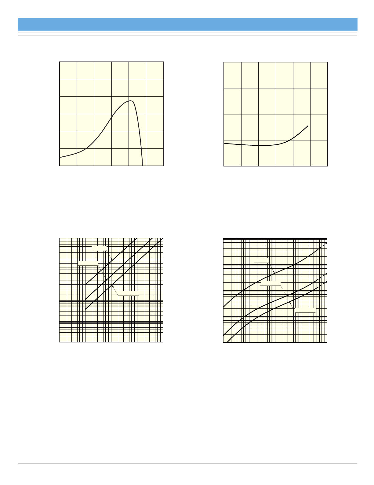
Spectral response
0.3
0.25
0.2
0.15
0.1
PHOTO SENSITIVITY (A/W)
0.05
0
190 400 600
WAVELENGTH (nm)
■■
■
■■
Rise time vs. load resistance
(Typ. Ta=25 ˚C)
800
KGPDB0034EA
■■
■
■■
Photo sensitivity temperature characteristic
+1.5
+1.0
+0.5
0
TEMPERATURE COEFFICIENT (%/˚C)
-0.5
190 400 600
WAVELENGTH (nm)
■■
■
■■
Dark current vs. reverse voltage
(Typ.)
800
KGPDB0035EA
10
ms
1
ms
100
µs
10
µs
RISE TIME
1
µs
100
ns
2
10
(Typ. Ta=25 ˚C, VR=0 V)
G2119
G1127-02
G1126-02
10
3
10
4
LOAD RESISTANCE (Ω)
10
1 nA
100 pA
10 pA
G2119
G1127-02
DARK CURRENT
1 pA
100
5
10
6
fA
0.01 0.10.001
(Typ. Ta=25 ˚C)
G1126-02
110
REVERSE VOLTAGE (V)
KGPDB0036EA
KGPDB0037EA
Page 3

GaAsP photodiode
G1126-02, G1127-02, G2119
■■
■
■■
Shunt resistance vs. ambient temperature
10 TΩ
1 TΩ
100 GΩ
10 GΩ
1 GΩ
SHUNT RESISTANCE
100 MΩ
10 MΩ
G2119
020-20
G1126-02
(Typ. VR=10 mV)
G1127-02
40 60 80
AMBIENT TEMPERATURE (˚C)
■■
■
■■
Dimensional outlines (unit: mm)
KGPDB0038EA
■■
■
■■
Short circuit current linearity
(Typ. Ta=25 ˚C, A light source fully illuminated)
0
10
-2
10
-4
10
-6
10
-8
10
-10
10
-12
10
OUTPUT CURRENT (A)
-14
10
DEPENDENT ON NEP
-1410-1210-1010-810-610-410-2
10
10
-16
-16
10
INCIDENT LIGHT LEVEL (lx)
RL=100 Ω
0
10
KGPDB0008EA
➀ G1126-02
PHOTOSENSITIVE
SURFACE
WINDOW
5.9 ± 0.1
0.45
LEAD
CONNECTED
TO CASE
9.1 ± 0.2
8.1 ± 0.1
5.08 ± 0.2
2.9
4.1 ± 0.2
20
KGPDA0006EA
➁ G1127-02
PHOTOSENSITIVE
SURFACE
WINDOW
10.5 ± 0.1
0.45
LEAD
CONNECTED
TO CASE
13.9 ± 0.2
12.35 ± 0.1
7.5 ± 0.2
5.0 ± 0.2
1.9
15
MARK ( 1.4)
KGPDA0007EA
Page 4

➂ G2119
PHOTOSENSITIVE
SURFACE
ACTIVE AREA
0.9
0.3
16.5 ± 0.2
GaAsP photodiode
15.0 ± 0.15
2.15 ± 0.1
0.1
G1126-02, G1127-02, G2119
0.5
LEAD
ANODE
TERMINAL MARK
10.5
15.1 ± 0.3
12.5 ± 0.2
13.7 ± 0.3
KGPDA0011EA
Information furnished by HAMAMATSU is believed to be reliable. However, no responsibility is assumed for possible inaccuracies or omissions.
HAMAMATSU PHOTONICS K.K., Solid State Division
1126-1 Ichino-cho, Hamamatsu City, 435-8558 Japan, Telephone: (81) 053-434-3311, Fax: (81) 053-434-5184, http://www.hamamatsu.com
U.S.A.: Hamamatsu Corporation: 360 Foothill Road, P.O.Box 6910, Bridgewater, N.J. 08807-0910, U.S.A., Telephone: (1) 908-231-0960, Fax: (1) 908-231-1218
Germany: Hamamatsu Photonics Deutschland GmbH: Arzbergerstr. 10, D-82211 Herrsching am Ammersee, Germany, Telephone: (49) 08152-3750, Fax: (49) 08152-2658
France: Hamamatsu Photonics France S.A.R.L.: 8, Rue du Saule Trapu, Parc du Moulin de Massy, 91882 Massy Cedex, France, Telephone: 33-(1) 69 53 71 00, Fax: 33-(1) 69 53 71 10
United Kingdom: Hamamatsu Photonics UK Limited: 2 Howard Cour t, 10 Tewin Road, Welwyn Garden City, Hertfordshire AL7 1BW, United Kingdom, Telephone: (44) 1707-294888, Fax: (44) 1707-325777
North Europe: Hamamatsu Photonics Norden AB: Smidesvägen 12, SE-171 41 Solna, Sweden, Telephone: (46) 8-509-031-00, Fax: (46) 8-509-031-01
Italy: Hamamatsu Photonics Italia S.R.L.: Strada della Moia, 1/E, 20020 Arese, (Milano), Italy, Telephone: (39) 02-935-81-733, Fax: (39) 02-935-81-741
Specifications are subject to change without notice. No patent rights are granted to any of the circuits described herein. ©2001 Hamamatsu Photonics K.K.
Cat. No. KGPD1005E01
Apr. 2001 DN
 Loading...