

Page 1
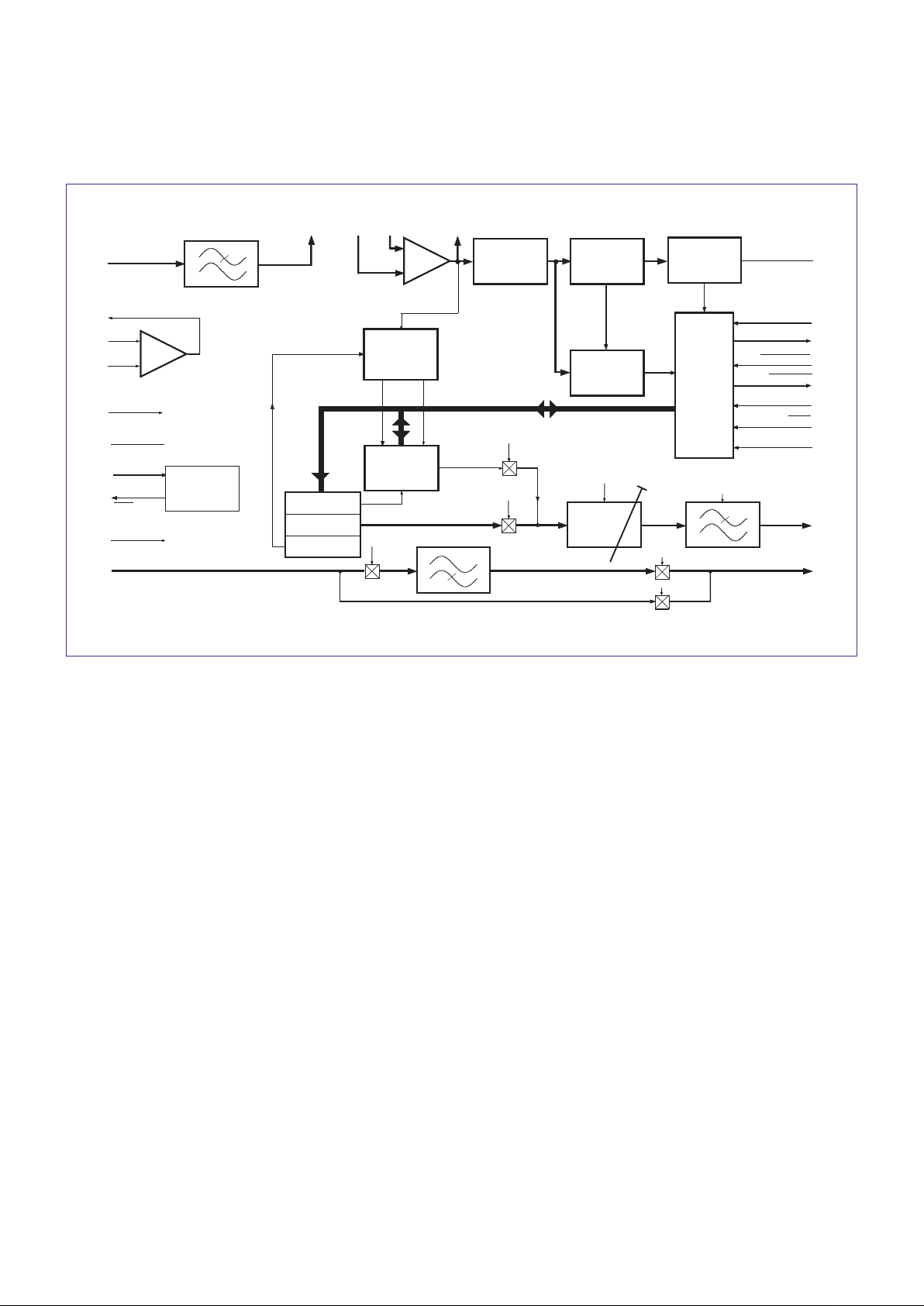
FX805 Sub-Audio
Signalling Processor
AUDIO IN
COMMAND DATA
C-BUS
INTERFACE
AND
CONTROL
LOGIC
REPLY DATA
SERIAL CLOCK
XTAL/CLOCK
NOTONE
ADDRESS SELECT
Tx LEVEL
ADJUST
Rx SUB-AUDIO
OUT
+
–
Rx AMP
COMPARATOR
AMP
Tx
SUB-AUDIO
OUT
AUDIO OUT
Rx SUB-AUDIO
IN
NOTONE
TIMER
DIGITAL
NOISE
FILTER
CLOCK
GENERATOR
DATA BUFFER
and
SHIFT REGISTER
SUB-AUDIO BANDSTOP
Variable
Bandwidth
NRZ Tx BAUD
RATE
V
DD
V
BIAS
V
SS
180Hz/260Hz
COMPARATOR
IN OUT
CHIP SELECT
WAKE
FREQUENCY
ASSESMENT
IN
OUT
NRZ
Rx Data
NRZ
Rx Baud Rate
CTCSS
Tx TONE
NRZ Rx
CLOCK RATE
NRZ Rx
DATA and
BAUD RATE
EXTRACTOR
+
–
Raw NRZ “Data”
CTCSS “Sub-Audio” Frequency
INTERRUPT
XTAL
Rx
Tx
NRZ Tx Data
Audio Signal Path
Audio By-Pass
Rx LOWPASS
Tx SUB-AUDIO LOWPASS
FREQUENCY
MEASUREMENT
(COUNTER)
Fig.1 FX805 Sub-Audio Signalling Processor
FX805 Sub-Audio Signalling Processor
A µProcessor controlled, sub-audio frequency signalling
processor to provide an outband audio and digital signalling
facility for PMR radio systems.
This device caters for the transmission and non-predictive
reception of:
●
Continuous Tone Controlled Squelch (CTCSS) tones
and other non-standard sub-audio frequencies.
●
Non-Return-to-Zero (NRZ) data to facilitate Continuous
Digitally Coded Squelch (CDCS/DPL
) system
operations.
To achieve these functions, the FX805 has on-chip:
●
A non-predictive CTCSS Tone Decoder and CDCS subaudio signal demodulator.
●
A CTCSS/NRZ Encoder with Tx level adjustment and
lowpass filter output stage with optional NRZ
pre-emphasis.
●
A selectable sub-audio bandstop filter.
●
A Notone (CTCSS Rx) period timer.
Setting of the FX805 functions and modes is by data
loaded from the µController to the controlling registers within
the device. Reply Data and Interrupt protocol keep the
µController up to date on the operational status of the
circuitry –– all via the “C-BUS” interface.
CTCSS tone data for transmission is generated within the
µController, loaded to CTCSS Tx Frequency Register,
encoded and output as a tone via the Tx Sub-Audio Lowpass
Filter.
Received non-predicted CTCSS tone frequencies are
measured and the resulting data, in the form of a 2-byte
data-word, is presented via the CTCSS Rx Frequency
Register to the µController for matching against a ‘look-up’
table. Noise filtering is provided to improve the signal quality
prior to measurement.
NRZ coded data streams for transmission, when
generated within a µController, are loaded to the NRZ Tx
Data Buffer and output, in 8-bit bytes, through the Lowpass
Filter circuitry as sub-audio signals. CDCS turn-off tones can
be added to the data signals by switching the FX805 to the
CTCSS transmit mode at the appropriate time.
NRZ coding is produced by the µController and translated
into sub-audio signals by the FX805.
Received NRZ data is filtered, detected and placed into
the NRZ Rx Data Register which is then available for transfer
one byte at a time, to the µController, for decoding by
software. Clock extraction circuitry is provided on chip and
Rx and Tx baud rates are selectable.
Provision is made in both hardware and system software
allocations to address two FX805 Sub-Audio Signalling
Processors consecutively to achieve multi-mode, duplex
operation.
The FX805 has a powersaving function which may be
controlled by software or a dedicated (Wake) input.
The FX805 is a low-power, 5-volt CMOS integrated circuit
and is available in 24-pin DIL cerdip and 24-pin/lead plastic
SMD packages.
DPL is a registered trademark of Motorola Inc.
Publication D/805/3 July 1994
Page 2
2
Pin Number Function
FX805
J/LG/LS
1
2
3
4
5
6
7
8
9
10
11
12
Xtal: The output of the on-chip clock oscillator. External components are required at this input when a
Xtal (f
XTAL
) input is used. See Figure 2.
Xtal/Clock: The input to the on-chip clock oscillator inverter. A Xtal or externally derived clock (f
XTAL
)
should be connected here. See Figure 2.
Address Select: This pin enables two FX805 devices to be used on the same “C-BUS,” providing fullduplex operation. See Tables 1 and 2.
Interrupt Request (IRQ): The output of this pin indicates an interrupt condition to the µController, by
going to a logic “0.” This is a “wire-or able” output, allowing the connection of up to 8 peripherals to 1
interrupt port on the µController. This pin has a low impedance pulldown to logic “0” when active and a
high impedance when inactive. The System IRQ line requires 1 pullup resistor to VDD. The conditions
that cause interrupts are indicated in the Status Register (Table 4) and are shown below:
Rx CTCSS Tone Measurement Complete CTCSS N
OTONE
Timer Expired
1 NRZ Rx Data Byte Received New NRZ Rx Data Received Before Last Byte Read
NRZ Tx Buffer Ready NRZ Data Transmission Complete
Serial Clock: The “C-BUS” serial clock input. This clock, produced by the µController, is used for
transfer timing of commands and data to and from the Sub-Audio Signalling Processor. See Timing
Diagrams.
Command Data: The “C-BUS” serial data input from the µController. Data is loaded to this device in
8-bit bytes, MSB (B7) first, and LSB (B0) last, synchronized to the Serial Clock. See Timing Diagrams.
Chip Select (CS): The “C-BUS” data loading control function. This input is provided by the
µController. Data transfer sequences are initiated, completed or aborted by the CS signal. See Timing
Diagrams.
Reply Data: The “C-BUS” serial data output to the µController. The transmission of Reply Data bytes
is synchronized to the Serial Clock under the control of the Chip Select input. This 3-state output is held
at high impedance when not sending data to the µController. See Timing Diagrams.
Tx Sub-Audio Out: The sub-audio output (pure or NRZ derived). Signals are band-limited, the Tx
Output Filter has a variable bandwidth, see Table 6. This output is at V
BIAS
(a) when the NRZ Encoder
is enabled but no data is being transmitted, (b) when the FX805 is placed in the Powersave All
condition.
Audio In: The input to the switched sub-audio bandstop (highpass) filter. This input is internally biased
and requires to be a.c. coupled by capacitor C
7
.
Audio Out: The output of the ‘audio signal path’ (filter or by-pass). This output is controlled by the
Control Register and when disabled is held at V
DD
/2.
V
SS
: Negative Supply (Signal Ground).
Page 3

3
Pin Number Function
FX805
J/LG/LS
13
14
15
16
17
18
19
20
21
22
23
24
“C-BUS” is CML’s proprietry standard for the transmission of commands and data between a
µ
Controller and DBS 800 microcircuits. It may be used with any µController, and can, if
desired, take advantage of the hardware serial I/O functions embodied into many types of
µ
Controller. The “C-BUS” data rate is determined soley by the µController.
Rx Amp (-) In: The inverting input to the on-chip Rx Input Amp. See Figures 2, 3 and 4.
Rx Amp (+) In: The non-inverting input to the on-chip Rx Input Amp.
Rx Amp Out: The output of the on-chip Rx Input Op-Amp. This circuit may be used, with external
components, as a signal amplifier and an anti-aliasing filter prior to the Rx Lowpass Filter, or for other
purposes. See Figure 2 for component details.
Rx Sub-Audio In: The received sub-audio (CTCSS/NRZ) input. This input is internally biased to V
DD
/2
and requires to be a.c. coupled or biased. See Figure 2 for component details.
Rx Sub-Audio Out: The output of the Rx Lowpass Filter. This output may be coupled into the on-chip
amplifier or comparator as required.
V
BIAS
: The internal circuitry bias line, held at VDD/2 this pin must be decoupled to VSS by capacitor C
8
(see Figure 2).
Comparator In (-): The inverting input to the on-chip “comparator” amplifier. See Figures 2, 3 and 4.
Comparator (+): The non-inverting input to the on-chip “comparator” amplifier. See Figures 2, 3 and 4.
Comparator Out: The output of the “comparator” amplifier. This node is also internally connected to
the input of the Digital Noise Filter (see Figure 1). When both decoders are Powersaved, this output is
at a logic “0.”
N
OTONE Timing: External RC components connected to this pin form the timing mechanism of a
NOTONE period timer. The external network determines the ‘charge-rate’ of the timer to VDD/2. Expiry of
the timer will cause an interrupt. This facility is only used in the CTCSS Rx mode.
Wake: This ‘real-time ’ input can be used to reactivate the FX805 from the ‘Powersave All’ condition
using an externally derived signal. The FX805 will be in a ‘Powersave All’ condition when both this pin
and Bit 0 of the Control Register are set to a logic “1.” Recovery from “Powersave All” is achieved by
putting either the Wake pin or the ‘Powersave All’ bit to logic “0,” thus allowing FX805 activation by the
µController or an external signal, such as R.S.S.I. or Carrier Detect.
V
DD
: Positive supply rail. A single +5-volt power supply is required. Levels and voltages within the Sub-
Audio Signalling Processor are dependant upon this supply.
NOTE: (i) Further information on external components and DBS 800 system integration of this
microcircuit are contained in the System Support Document.
(ii) A glossary of abbreviations used in this document is supplied.
(iii) Guidance upon the generation and manipulation of NRZ Rx and Tx data is given in DBS
800 Application Support Document.
Page 4
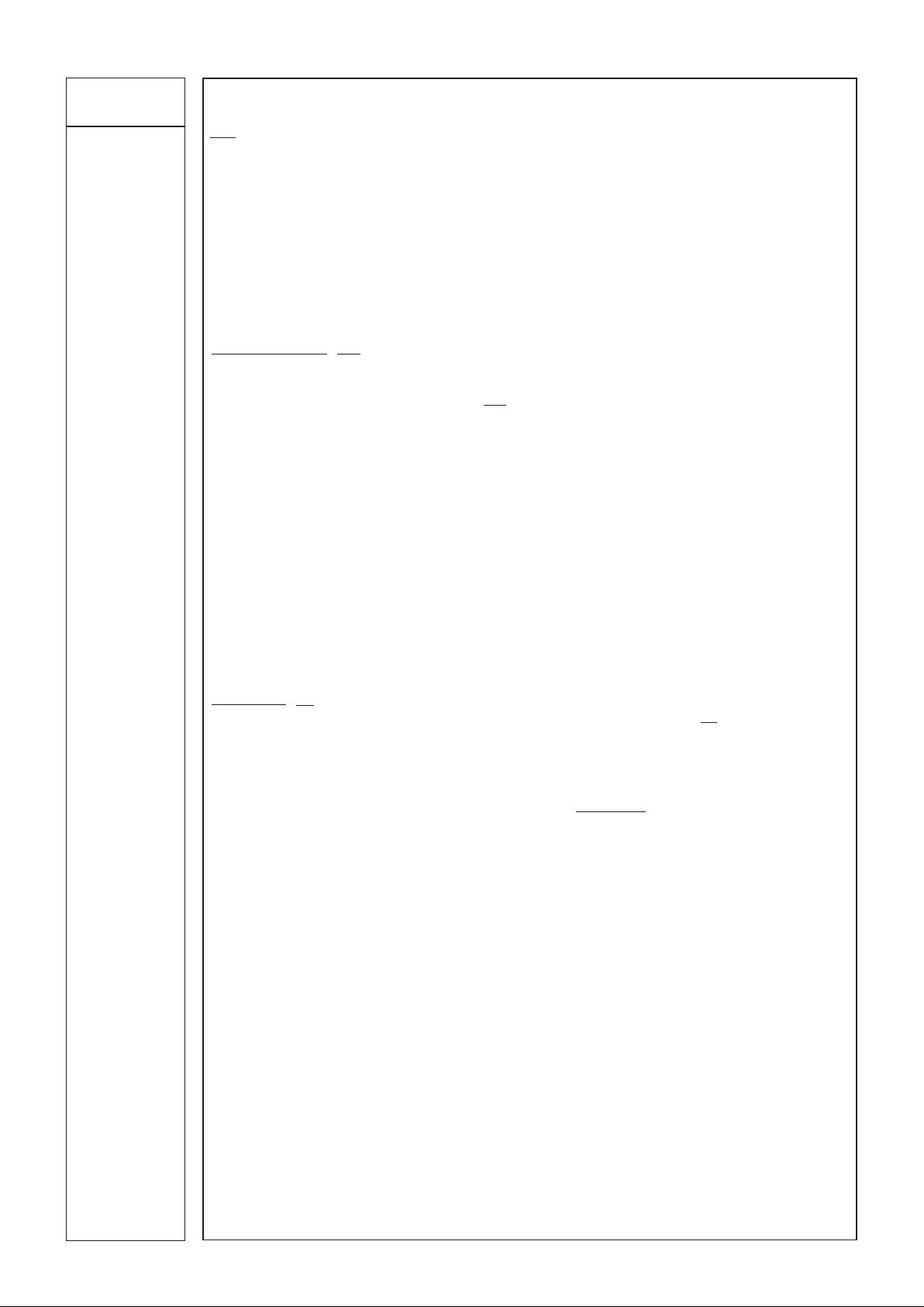
4
Application Information
External Components
XTAL/CLOCK
V
DD
SEE INSET
V
SS
NOTONEADDRESS SELECT
13
14
15
16
17
18
19
20
21
22
23
24
1
2
3
4
5
6
7
8
9
10
11
12
FX805J
SERIAL CLOCK
COMMAND DATA
REPLY DATA
Tx SUB-AUDIO OUT
AUDIO IN
AUDIO OUT
V
SS
COMPARATOR OUT
COMPARATOR IN (+)
COMPARATOR IN (-)
Rx AMP IN (-)
Rx SUB-AUDIO OUT
Rx AMP IN (+)
Rx SUB-AUDIO IN
Rx AMP OUT
V
SS
*
WAKE
XTAL
CS
V
DD
C
8
C
7
R
8
R
7
R
6
C
5
C
6
R
4
V
BIAS
C
3
R
3
D1D
2
R
5
C
4
R
2
IRQ
2
1
XTAL/CLOCK
V
SS
FX805J
INSET
XTAL
R
1
X
1
C
2
C
1
C6= 1.0µF
C
7
0.1µF
C
8
1.0µF
C
9
Fig.4
D
1
silicon small sig
D
2
silicon small sig
X1f
XTAL
4.00MHz
R9= Fig.4
R
10
Fig.4
R
11
Fig.4
C
1
33.0pF
C
2
33.0pF
C
3
1.5µF
C
4
15.0µF
C
5
1.0µF
Component Value
R1= 1.0MΩ
R
2
360kΩ
R
3
10.0kΩ
R
4
150kΩ
R
5
100kΩ
R
6
150kΩ
R
7
22.0kΩ
R
8
360kΩ
Fig.2 Recommended External Components
Notes
on external components and connections
1. Xtal/clock circuitry components shown INSET are
recommended in accordance with CML Application Note
D/XT/2 December 1991. The DBS 800 System
Information Document contains additional notes on Xtal/
clock distribution and frequencies.
2. R
8
is a System Component. Its value is chosen, for
example, with the FX806 Modulation Summing
Amplifier, to provide a sub-audio signal level of -11.0dB
to the system modulator.
3. Components R
6
and C6 are NOTONE timing components.
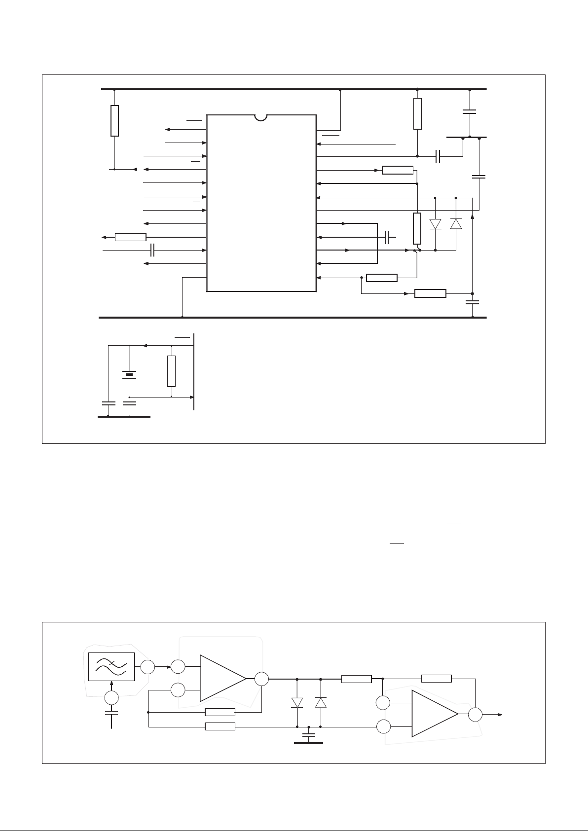
With reference to Figure 2, Figures 3 and 4 show in detail recommended alternative component configurations for the FX805.
14
+
13
–
17
Rx AMP IN
COMPARATOR IN
COMPARATOR OUT
FX805
Rx AMP
FX805
COMPARATOR
20
21
19
D.C. RESTORATION
+
–
HYSTERESIS
R
2
R
5
C
4
V
SS
D
2
D
1
R
3
R
4
FX805 Rx LPF
16
C
3
Rx Sub-Audio Input
15
Fig.3 Employment of FX805 Input Components
4. R2 and R5 are dependant upon the input signal level.
Values given are for the specified composite signal.
5. R7 is used as the DBS 800 system common-pullup for
the “C-BUS” Interrupt Request (IRQ) line, the optimum
value of this component will depend upon the circuitry
connected to the IRQ line.
Page 5
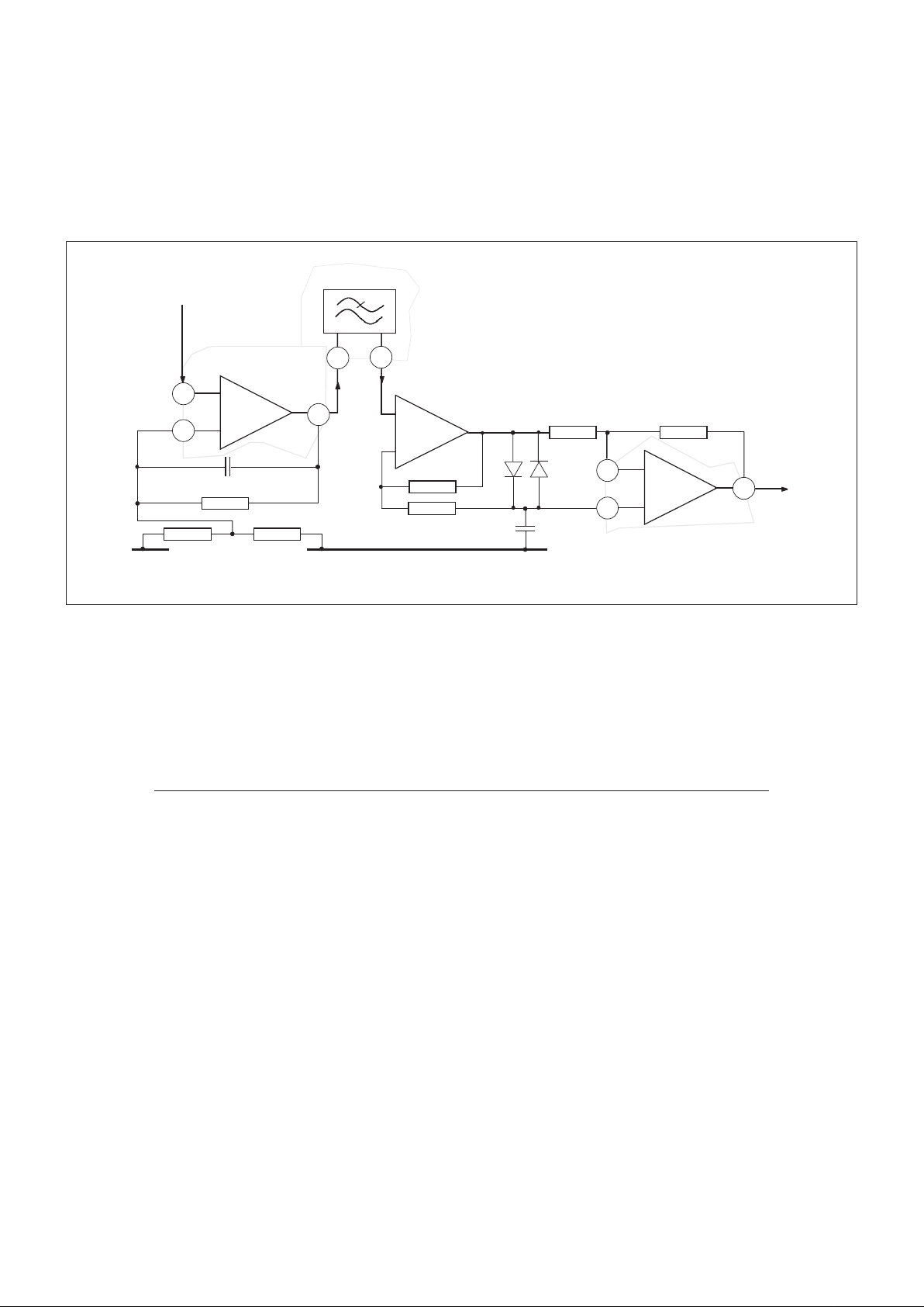
5
Application Information ......
External Components ......
COMPARATOR IN
14
+
13
–
Rx AMP IN
From
Rx Discriminator
15
COMPARATOR OUT
FX805
Rx AMP
20
21
19
D.C. RESTORATION
HYSTERESIS
R
2
R
5
C
4
V
SS
D
2
D
1
R
3
R
4
+
–
+
–
17
V
DD
C
9
R
9
R
10
R
11
FX805
COMPARATOR
EXTERNAL
OP-AMP
16
FX805 Rx LPF
Fig.4 FX805 Input Components Using an External Op-Amp
Using an External Op-Amp
For d.c. coupling the FX805 to the receiver’s discriminator
output when using NRZ communication, it is recommended
that an additional, external Op-Amp is employed as
configured in Figure 4. This configuration will allow long
sequences of logic “1
s
” or “0s” to be successfully decoded
(eg. LTR trunking systems).
Figure 3 shows an input component configuration for use
generally for CTCSS signal and NRZ data reception.
Input coupling capacitor C
3
is required because the Rx
Sub-Audio Input is held at V
BIAS
during all powered conditions
of the FX805. Diodes D1 and D2 can be any silicon smallsignal diode.
FX805 Operational Modes
NRZ Tx (Encoding)
The NRZ Encoder is formed by a shift register and the Tx
Sub-Audio Lowpass Filter. Data loaded from the Command
Data line is output one 8-bit byte at a time from the NRZ Tx
Data Register. The output data-signal level may be adjusted
and filtered. Data may be pre-emphasized via a “C-BUS”
command. The Tx baud rate is programmed as the NRZ Tx
Baud Rate (R
NRZ Tx
) (Table 5).
CTCSS Tx (Encoding)
The CTCSS Tone Encoder comprises a clock-divider
programmed by an 11-bit binary number (Q) loaded to the
CTCSS Tx Frequency Register (Table 5) via the “C-BUS”
Command Data line.
The square-wave output of the encoder is fed through the
Tx Level Adjust variable gain block to the Tx Sub-Audio
Lowpass Filter, a variable bandwidth circuit controlled by
4-bits (P) of the CTCSS Tx Frequency Register. The Tx SubAudio output is a sine-wave. Standard and non-standard
sub-audio tones are available, a ‘CDCS’ turn-off tone may be
generated.
NRZ Rx (Decoding)
Input (NRZ type) sub-audio signals are filtered and the
data clock extracted. Decoded data is serially loaded into a
shift register buffer. This data is output one 8-bit byte at a
time as Reply Data from the NRZ Rx Data Register (Page
14) to the µController. The expected Rx baud rate is
programmed as the NRZ Rx Baud Rate (R
NRZ Rx
) (Table 5).
Any codeword recognition can be carried out by software.
CTCSS Rx ( Decoding)
Received CTCSS signals are filtered, coherence is
increased by the digital noise filter. The quality of the signal
is assessed by measurement of the cycle-to-cycle period
variance and, provided it is sufficiently good, the frequency is
measured over a period of 122.64 milliseconds.
If the average signal quality is consistently too low, NOTONE
is indicated, if not, the input frequency is precisely indicated
in the CTCSS Rx Frequency Register in a binary form as
shown in Figure 6.
As any single sub-audio tone within the specified range
may be selected, this would enable a ‘CDCS’ turn-off tone
(of 134Hz) to be decoded whilst operating in the NRZ Rx
mode.
The output resistance (open loop) of the on-chip Rx Amp
is ≈ 6kΩ. In the configuration shown in Figure 3, the (Rx
Amp) RC time-constant is therefore 90ms. If this period is
too long for some systems, ie. those employing half-duplex,
short data bursts, an external amplifier should be considered
in place of the FX805 on-chip Rx Amp.
LTR is a registered trademark of E.F. Johnson Company
Components R9, R
10
and R11 should be calculated to
provide an accurate potential of 2.5V d.c. (equal to V
BIAS
) at
pin-junction 15/16 when using a discriminator input. C9 is an
optional component which, if additional filtering is required,
should be calculated, with R9 to provide a lowpass cut-off
frequency (fCO) of 500Hz.
Page 6

6
Controlling Protocol
Control of the FX805 Sub-Audio Signalling Processor's operation is by communication between the µController and the
FX805 internal registers on the “C-BUS,” using Address/Commands (A/Cs) and appended instructions or data (see Figure 9).
The use and content of these instructions is detailed in the following paragraphs and tables. The Address Select input enables
the addressing of 2 separate FX805s on the “C-BUS” to provide full-duplex multi-mode signalling.
Address/Commands
The first byte of a loaded data sequence is always
recognized by the “C-BUS” as an Address/Command (A/C)
byte. Instruction and data transactions to and from this
device consist of an Address/Command byte followed by
either:
(i) further instructions or data or,
(ii) a Status or data Reply.
Instructions and data are loaded and transferred, via
“C-BUS,” in accordance with the timing information given in
Figures 9 and 10.
Placing the Address Select input at a logic “0” will address
FX805 No.1, a logic “1” will address FX805 No.2.
Tables 1 and 2 show the list of A/C bytes relevant to the
FX805. A complete list of DBS 800 “C-BUS” Address
allocations is published in the System Support Document.
Command Address/Command (A/C) Byte + Data
Assignment Hex. Binary Byte/s
MSB LSB
General Reset 01 00000001
Write to Control Reg. 78 01111000 + 1 byte Instruction to Control Reg.
Read Status Reg. 79 01111001 + 1 byte Reply from Status Reg.
Read CTCSS Rx Frequency Reg. 7A 01111010 + 2 byte Reply of CTCSS Rx data
Write to CTCSS Tx Frequency/ 7B 01111011 + 2 byte Instruction for Tx Frequency
NRZ Baud Rate Reg. and NRZ Tx/Rx baud rates
Read NRZ Rx Data Reg. 7C 01111100 + 1 byte binary data Reply
Write to NRZ Tx Data Reg. 7D 01111101 + 1 byte binary data Command
Write to Gain-Set Reg. 7E 01111110 + 1 byte Instruction for Tx Output
Table 2 – FX805 No.2 “C-BUS” Address/Commands
Address Select input at a logic “1”
Command Address/Command (A/C) Byte + Data
Assignment Hex. Binary Byte/s
MSB LSB
General Reset 01 00000001
Write to Control Reg. 70 01110000 + 1 byte Instruction to Control Reg.
Read Status Reg. 71 01110001 + 1 byte Reply from Status Reg.
Read CTCSS Rx Freq. Reg. 72 01110010 + 2 byte Reply of CTCSS Rx data
Write to CTCSS Tx Frequency/ 73 01110011 + 2 byte Instruction for Tx Frequency
NRZ Baud Rate Reg. and NRZ Tx/Rx baud rates
Read NRZ Rx Data Reg. 74 01110100 + 1 byte binary data Reply
Write to NRZ Tx Data Reg. 75 01110101 + 1 byte binary data Command
Write to Gain-Set Reg. 76 01110110 + 1 byte Instruction for Tx Output
Table 1 – FX805 No.1 “C-BUS” Address/Commands
Address Select input at a logic “0”
FX805 Internal Registers
FX805 internal registers are detailed below:
Control Register (70
H
/78H) – Write only, control and
configuration of the FX805.
Status Register (71
H
/79H) – Read Only, reporting of device
functions.
CTCSS Rx Frequency Register (72
H
/7AH) – Read Only,
a 2-byte binary word indicating the frequency of the
received sub-audio input.
CTCSS Tx Frequency / NRZ Tx or Rx Baud Rate Register
(73H/7B
H
) – Write Only, a 2-byte command to set the
relevant parameters.
NRZ Rx Data Register (74H/7CH) – Read Only, a single-byte
of received NRZ data.
NRZ Tx Data Register (75
H
/7DH) – Write Only, to load a
single-byte of NRZ data for transmission one byte at a
time.
Gain-Set Register (76H/7EH) – Write Only, a single byte to
set the gain of the Tx Lowpass Filter.
Page 7

7
Controlling Protocol ......
“Write to Control Register” – A/C 70
H
(78H), followed by 1 byte of Command Data.
Table 3 (below) shows the configurations available to the FX805. Bits 5, 6 and 7 are used together to Enable and Powersave
circuit sections as required.
Setting
MSB
765
000
001
010
011
100
101
110
111
4
1
0
3
1
0
2
1
0
1
1
0
0
1
0
General Reset
Upon Power-Up the “bits” in the FX805 registers will be
random (either “0” or “1”). A General Reset Command (01H)
will be required to “reset” all microcircuits on the
“C-BUS,” and has the following effect upon the FX805.
Control Register Set as 00
H
Status Register Set as 00
H
N
OTONE
Timer Discharged
Warning – The following FX805 register configurations are
not affected by a General Reset command:
CTCSS Rx Frequency
CTCSS Tx Frequency/NRZ Baud Rate Register
NRZ Rx Data Register
NRZ Tx Data Register
Gain-Set Register
Note that setting the Control Register in this way (General
Reset) will set the FX805 to the CTCSS Decode mode and
overwrite a “Powersave All” instruction.
It should also be considered that a General Reset
command will reset ALL DBS 800 microcircuits operating on
the “C-BUS.”
Glossary of Abbreviations
Below is a list of abbreviations used within this Data Sheet.
CDCS Continuous Digitally Coded Squelch
CTCSS Continuous Tone Controlled Squelch
DPL
Digital Private Line
LTR
Logic Trunked Radio
NRZ Non-Return-to-Zero data levels
f
CO
Filter cut-off frequency
f
CTCSS IN
Sub-Audio Rx frequency
f
CTCSS OUT
Sub-Audio Tx frequency
f
TONE
Tone frequency
f
XTAL
Xtal/clock frequency
R
NRZ Rx
NRZ Rx baud rate
R
NRZ Tx
NRZ Tx baud rate
S
INPUT
Audio input signal
Control Bits
Transmitted First
Functions Enabled Functions Powersaved
CTCSS Decoder NRZ Decoder and Both Encoders
NRZ Decoder CTCSS Decoder and Both Encoders
CTCSS Encoder All Decoders
NRZ Encoder All Decoders
CTCSS Encoder and Decoder NRZ Encoder and Decoder
NRZ Encoder and CTCSS Decoder None
NRZ Decoder and CTCSS Decoder All Encoders
NRZ Decoder All Encoders (except Tx Sub-Audio LPF)
and CTCSS Decoder
Enable Audio Output – Used with Bit 3
Disable Audio Output – Output to V
BIAS
Enable Sub-Audio Bandstop Filter (Audio Signal Path)
By-pass Sub-Audio Bandstop Filter
Enable All FX805 Interrupts
Disable All FX805 Interrupts
Set Rx Lowpass Filter bandwidth to 180Hz – For low CTCSS Tones or NRZ Data
Set Rx Lowpass Filter bandwidth to 260Hz
All Encoders and Decoders Powersaved (Powersave All)
All Encoders and Decoders Enabled unless individually Powersaved
Table 3 Control Register
Page 8

8
Controlling Protocol ......
Status Bit
MSB
7 , 6
5
4
3
2
1
0
Logic
“0”
“0”
“0”
“0”
“0”
“0”
“0”
Cleared By
Not used
1. Write to NRZ Tx Data Reg. or,
2. General Reset or,
3. NRZ Encoder Powersave.
1. Write to NRZ Tx Data Reg. or,
2. General Reset or,
3. NRZ Tx Powersave.
1. Read NRZ Rx Data Reg. or,
2. General Reset or,
3. NRZ Decoder Powersave.
1. Read NRZ Rx Data Reg. or,
2. General Reset or,
3. NRZ Decoder Powersave.
1. Read Status Register or,
2. General Reset or,
3. CTCSS Decoder Powersave.
1. Read Status Register or,
2. General Reset or,
3. CTCSS Decoder Powersave.
Logic
“0”
“1”
“1”
“1”
“1”
“1”
“1”
Set By
Received First
Not used
NRZ data transmission
complete. No new data loaded.
NRZ Tx Data Buffer ready for
next data byte.
New NRZ Rx data received
before last byte was read.
1 byte of NRZ Rx data
received.
NOTONE Timer period expired.
Rx Tone Measurement
complete.
Table 4 Status Register
“Read Status Register” – A/C 71
H
(79H), followed by 1 byte of Reply Data.
The Status Register indicates the operational condition of the FX805. Bits 0 to 5 are set individually to indicate specific
actions within the device. When a Status Bit is set to a logic “1,” an Interrupt Request (IRQ) output is generated. A read of the
Status Register will reset the interrupt condition and ascertain the state of this register.
Table 4 (below) shows the conditions indicated by the Status Bits.
Measurement Period
R
Complete
Input
Cycle
Complete
Input
Cycle
Complete
Input
Cycle
Complete
Input
Cycle
Complete
Input
Cycle
FILTERED and DOUBLED SUB-AUDIO INPUT SIGNAL
Measuring
Clock
Cycles
N
CTCSS IN
2 x f
Fig.5 Measurement of a CTCSS Rx Frequency
“Read CTCSS Rx Frequency Register” – A/C 72
H
(7AH), followed by 2 bytes of Reply Data.
Measurement of CTCSS Rx Frequency (f
CTCSS IN
)
The input sub-audio signal (f
CTCSS IN
), is filtered and
measured in the Frequency Counter over the “measurement
period” (122.64ms).
The measuring function counts the number of complete
input cycles occurring within the measurement period and
then the number of measuring-clock cycles necessary to
make up the period.
When the measurement period of a successful decode
is complete, the Rx Tone Measurement bit in the Status
Register, and the Interrupt bit are set.
The CTCSS Rx Frequency Register will now indicate
the sub-audio signal frequency (f
CTCSS IN
) in the form of 2
data bytes (1 and 0) as illustrated in Figure 6.
Page 9

9
R = INT 511 – N x f
XTAL
+ 0.5 [3]
1920 x f
CT CSS IN
Controlling Protocol ......
“Read CTCSS Rx Frequency Register” ......
The Integer (N) – Byte 1
A binary number representing ‘twice the number of
complete input sub-audio cycle periods’ counted during the
measurement period of 122.64ms
The Remainder (R) – Byte 0
A binary number representing the remainder part, R,
of 2 x Sub-Audio Input Frequency. ‘R = number of specified
measuring-clock cycles’ required to complete the specified
measurement period (See N). The clock-cycle frequency is
4166.6Hz
15 14 13 12 11 10 9 8
Byte 0
(REPLY DATA
)
(LSB) – TRANSMITTED LAS
T
Integer (N)
Byte 1
“0” “0”
Remainder (R)
(REPLY DATA)
(MSB) – TRANSMITTED FIRST
“0” “0”
7654 321 0
Fig. 6 Format of the CTCSS Rx Frequency Register
CTCSS Rx Frequency Register
Figure 6 (above) shows the format of the CTCSS Rx
Frequency Register.
Bits 8 (LSB) to 13 (MSB) are used to represent the Integer
(N). From Byte 1, valid values of N = 16 ≤ N ≤ 61.
ie. values of N less than 16 and greater than 61 are not
within the specified frequency band.
Bits 0 (
LSB) to 5 (MSB) (Byte 0) are used to represent the
Remainder (R). From Byte 0, valid values of R = ≤ 31.
This register is not affected by the General Reset
command (01H) and may adopt any random configuration at
Power-Up.
CTCSS Rx Frequency Measurement Formulæ
To assist in the production of ‘look-up’ tables and limit-values in the µController and provide guidance upon the determination
of N and R from a measured CTCSS frequency, the following formulæ show the derivation of the CTCSS Rx Frequency
(f
CTCSS IN
) from the measured data bytes (N and R).
If there is no signal or the signal is of a consistently poor
quality, the N
OTONE Timer will start to charge via the timing
components. When the timing period has expired (at VDD/2),
an Interrupt and a Status bit (NOTONE Timer Expired) are
generated. This is a one-shot function and is reset by a “Tone
Measurement Complete” interrupt.
NOTONE Timing
The input sub-audio signal is monitored by the Frequency
Assessment circuitry. Before any NOTONE action is enabled,
the FX805 must have achieved at least one successful “Tone
Measurement Complete” action.
Examples (f
XTAL
= 4.00MHz): f
CTCSS IN
= 100Hz N = 24 R = 11; f
CTCSS IN
= 250Hz N = 61 R = 3
f
CTCSS IN
In the measurement period of 122.64ms there are N
cycles at 2 x f
CTCSS IN
and R clock-cycles at 4166.6Hz, for any
input frequency.
So
f
CTCSS IN
=N x f
XTAL
Hz [1]
1920 x (511 -R)
N = INT (1920 x 511 x f
CTCSS IN
) [2]
f
XTAL
Calculate N first
Page 10

10
Controlling Protocol ......
“Write to CTCSS Tx Frequency/NRZ Baud Rate Register” – A/C 73
H
(7BH), followed by 2 bytes of
Command Data.
The information loaded to this register will set either the:
(a) CTCSS Tx Tone Frequency f
CTCSS OUT
(b) NRZ Tx Baud Rate R
NRZ Tx
(c) NRZ Rx Baud Rate R
NRZ Rx
The chosen mode for this register (a, b or c) is determined by the FX805 operational mode enabled by the Control Register
(Table 3), as shown in the table below.
Control Register Bits FX805 Mode CTCSS Tx/NRZ Baud Rate
7 6 5 Enabled Register Function
0 0 0 CTCSS Decode
0 0 1 NRZ Decode NRZ Rx Baud Rate
0 1 0 CTCSS Encode CTCSS Tx Frequency
0 1 1 NRZ Encode NRZ Tx Baud Rate
1 0 0 CTCSS Encode and Decode CTCSS Tx Frequency
1 0 1 NRZ Encode and CTCSS Decode NRZ Tx Baud Rate
1 1 0 NRZ and CTCSS Decode NRZ Rx Baud Rate
1 1 1 NRZ Decode NRZ Rx Baud Rate
Table 5 CTCSS Frequency/NRZ Baud Rate Register Configurations
Data Format
Data is transmitted, via “C-BUS,” to this register as 2 bytes of Command Data (1 and 2) distributed as command words P and
Q, in the form illustrated in Figure 7. This register is not affected by the General Reset command (01H) and may adopt any
random configuration at Power-Up.
Command Words P and Q
With reference to Figure 7, the two data words, P and Q, loaded to this register are interpreted as:
P = a binary number to set the Tx Sub-Audio Lowpass Filter bandwidth (applicable to NRZ Encode and CTCSS
Encode modes).
Q = a binary number to set the frequency or baud rate of the selected function (see Table 5).
Command Word ‘P’
Bits LSB
15 14 13 12 ‘P’ LPF Bandwidth
0 0 1 0 2 300Hz
0 0 1 1 3 200Hz
0 1 0 0 4 150Hz
0 1 0 1 5 120Hz
0 1 1 0 6 100Hz
0 1 1 1 7 85.7Hz
1 0 0 0 8 75Hz
Table 6 Valid Values of ‘P’
Bits 12 to 15 are used to produce the data word ‘P’ as
shown in Table 6 (left). The cut-off frequency f
CO
(0.5dB
point) of the Tx Sub-Audio Lowpass Filter is calculated as:
fCO = f
XTAL
32 x 208.33 x ‘P’
so ‘P’ = f
XTAL
32 x 208.33 x f
CO
Table 6 is given as an example and calculated using a Xtal/
clock (f
XTAL
) frequency of 4.00MHz. As illustrated, only values
of ‘P’ of
2 to 8
are usable.
15 14 13 12 11 10 9 8
Byte 0
(COMMAND DATA
)
(LSB) – LOADED LAS
T
P
Byte 1
Q
(COMMAND DATA)
(MSB) – LOADED FIRST
“0”
7654 321 0
Fig.7 Format of the CTCSS Tx Frequency/NRZ Baud Rate Register
Page 11

11
Controlling Protocol ......
Command Word ‘Q’
With reference to Figure 7, Bits 0 to 10 are used to produce the data word ‘Q’ which sets one of the parameters described
below. As can be seen, command word ‘Q’ could be used to produce a word whose value would produce a parameter outside
that specified, care should be taken not to do this. Examples for limits of ‘Q’ in each operational configuration are included. ‘Q’
= 0 is not valid in the following calculations. Bit 11 is not used and must be set to logic “0”.
Example Limits
f
CTCSS OUT
= 67Hz
so ‘Q’ = 1866 “11101001010”
f
CTCSS OUT
= 250Hz
so ‘Q’ = 500 “00111110100”
R
NRZ Tx
= 67 bits/sec
so ‘Q’ = 1866 “11101001010”
R
NRZ Tx
= 300 bits/sec
so ‘Q’ = 417 “00110100001”
R
NRZ Rx
= 100 bits/sec
so ‘Q’ = 114 “00001110010”
R
NRZ Rx
= 300 bits/sec
so ‘Q’ = 38 “00000100110”
(a) CTCSS Tx Tone Frequency (f
CTCSS OUT
)
f
CTCSS OUT
=f
XTAL
Hz
32 x ‘Q’
so ‘Q’= f
XTAL
Hz
32 x f
CTCSS OUT
(b) NRZ Tx Baud Rate (R
NRZ Tx
)
R
NRZ Tx
=f
XTAL
bits/sec
32 x ‘Q’
so ‘Q’= f
XTAL
32 x R
NRZ Tx
(c) NRZ Rx Baud Rate (R
NRZ Rx
)
R
NRZ Rx
=f
XTAL
bits/sec
32 x 11 x ‘Q’
so ‘Q’= f
XTAL
352 x R
NRZ Rx
“Write to CTCSS Tx Frequency/NRZ Baud Rate Register” ......
Page 12

12
Controlling Protocol ......
“Read NRZ Rx Data Register” – A/C 74
H
(7CH), followed by 1 byte of Reply Data.
Received NRZ data bits are organized into bytes and
made available to the µController via the Reply Data line. As
8 bits are received into this register an interrupt is generated
to indicate that a complete byte has been received, this byte
must be read before the arrival of the last (8th) bit of the next
incoming byte, if this is not done, an interrupt to indicate this
condition will be generated and the previous Rx data is
discarded (See Table 4, Status Register, Bits 2 and 3).
Word synchronization is not provided. Byte
synchronization and any codeword recognition will be
performed by the host µController. The Rx baud rate is set
by writing to the CTCSS Tx Frequency/NRZ Baud Rate
Register (73
H
/7BH). The first bit received is the first bit sent to
the µController.
This register is not affected by the General Reset
command (01H) and may adopt any random configuration at
Power-Up.
“Write to NRZ Tx Data Register” – A/C 75
H
(7DH), followed by 1 byte of Command Data.
Transmission is terminated, the Tx Sub-Audio Output placed
at V
BIAS
, and an interrupt generated if the next byte is not
loaded within 7 bit periods. (See Table 4, Status Register,
Bits 4 and 5).
This register is not affected by the General Reset
command (01H) and may adopt any random configuration at
Power-Up.
A byte for transmission is loaded from the “C-BUS”
Command Data line with this A/C. The first data-bit received
via the “C-BUS” is transmitted first. This transmitter
operation is non-inverting.
The first data-byte loaded after the NRZ Encoder is
enabled (Control Register) initiates the transmission
sequence and an interrupt will be generated when the NRZ
Tx Data Buffer is ready for the next data-byte.
Subsequently, interrupts occur for every 8 bits transmitted.
“Write to Gain-Set Register” – A/C 76
H
(7EH), followed by 1 byte of Command Data.
Setting
MSB
76 5 4
0000
3
1
0
210
000
001
010
011
100
101
110
111
Gain Setting
Transmitted Bit 7 First
These 4 Bits Must be “0”
Pre-Emphasis Setting
1.72dB Gain Enabled
1.72dB Gain Disabled
Tx Level Adjust Gain Setting
-2.58 dB
-1.72 dB
-0.86 dB
0dB
+0.86 dB
+1.72 dB
+2.58 dB
Not Used
Table 7 Gain-Set Register Settings
Fig.8 Gain-Set with Pre-Emphasis
NRZ Tx DATA
BIT PERIODS
GAIN-SET NRZ Tx DATA with PRE-EMPHASIS ENABLED
Gain-Set
+1.72dB
Gain-Set
+1.72dB
Gain-Set
+1.72dB
Gain-Set
+1.72dB
The Gain-Set Register Settings
The settings of this register control the CTCSS and NRZ
signal level that is presented at the Tx Sub-Audio Output.
Bit 3, when enabled, is used to produce a pre-emphasis
effect on the NRZ Tx Data by increasing the gain of the data
bit before a level change (Figure 8 below), by 1.72dB to
make that data pulse level slightly more positive (or
negative). The signal level will be 1.72dB greater than that
set by Bits 0 to 2. If the Tx Sub-Audio Output level is set to
+2.58dB, the pre-emphasized level will be +4.3dB.
The pre-emphasis function, will remain enabled until
disabled by setting Bit 3 to a logic “0.” If this function remains
enabled when using the CTCSS Encoder the output signal
level may be adversely affected, therefore this function
should only be enabled when in the NRZ Encode mode.
This register is not affected by the General Reset
command (01
H
) and may adopt any random configuration at
Power-Up.
Page 13

13
Timing Information
70% V
DD
30% V
DD
t
CL
t
CH
t
CDS
t
CDH
t
RDS
t
CK
t
RDH
SERIAL CLOCK
(from
µ
C)
COMMAND DATA
(from
µ
C)
REPLY DATA
(to
µ
C)
Fig.10 “C-BUS” Timing Relationships
NOT TO SCALE
Parameter Min. Typ. Max. Unit
t
CSE
2.0 – – µs
t
CSH
4.0 – – µs
t
CSOFF
2.0 – – µs
t
NXT
4.0 – – µs
t
CK
2.0 – – µs
t
CH
500 – – ns
t
CL
500 – – ns
t
CDS
250 – – ns
t
CDH
0––ns
t
RDS
250 – – ns
t
RDH
50.0 – – ns
t
HIZ
– – 2.0 µs
Notes
(1) Command Data is transmitted to the peripheral MSB (bit 7) first, LSB (bit 0) last.
Reply Data is read from the FX805 MSB (bit 7) first, LSB (bit 0) last.
(2) Data is clocked into the FX805 and into the µController on the rising Serial Clock edge.
(3) Loaded data instructions are acted upon at the end of each individual, loaded byte.
(4) To allow for differing µController serial interface formats, the FX805 will work with either polarity Serial
Clock pulses.
Timing Diagrams
Figure 9 shows the timing parameters for two-way communication between the µController and the FX805 on the “C-BUS.”
Figure 10 shows, in detail, the timing relationships for “C-BUS” information transfer.
SERIAL CLOCK
COMMAND DATA
t
CSE
t
NXT
t
CSOFF
t
CSH
t
HIZ
ADDRESS/COMMAND
BYTE
FIRST DATA BYTE LAST DATA BYTE
76543210 76543210 76543210
76543210
MSB LSB
CHIP SELECT
LAST REPLY DATA BYTE
t
NXT
t
CK
REPLY DATA
76543210
MSB LSB
FIRST REPLY DATA BYTE
Logic level is not important
Fig.9 “C-BUS” Timing Information
NOT TO SCALE
Page 14

14
Specification
Absolute Maximum Ratings
Exceeding the maximum rating can result in device damage. Operation of the device outside the operating limits is not implied.
Supply voltage -0.3 to 7.0V
Input voltage at any pin (ref V
SS
= 0V) -0.3 to (V
DD
+ 0.3V)
Sink/source current (supply pins) +/- 30mA
(other pins) +/- 20mA
Total device dissipation @ T
AMB
25°C 800mW Max.
Derating 10mW/°C
Operating temperature range: FX805J -40°C to +85°C (cerdip)
FX805LG/LS -40°C to +85°C (plastic)
Storage temperature range: FX805J -55°C to +125°C (cerdip)
FX805LG/LS -40°C to +85°C (plastic)
Operating Limits
All device characteristics are measured under the following conditions unless otherwise specified:
V
DD
= 5.0V. T
AMB
= 25°C. Xtal/Clock f
XTAL
= 4.0MHz. Audio Level 0dB ref: = 308mVrms @ 1kHz.
Composite Signal = 308mVrms @ 1kHz + 75mVrms Noise + 31mVrms Sub-Audio Signal.
Noise Bandwidth = 5kHz Band Limited Gaussian.
Characteristics See Note Min. Typ. Max. Unit
Static Values
Supply Voltage 4.5 5.0 5.5 V
Supply Current (All Functions Enabled) – 5.0 – mA
(Decoders Only Enabled) – 1.9 – mA
(Powersave All) – 0.9 – mA
Analogue Impedances
Rx Sub-Audio Input 350 – – kΩ
Audio Input 350 – – kΩ
Audio By-Pass Switch ‘On’ 5 – 2.0 – kΩ
Audio By-Pass Switch ‘Off’ 5 1.0 10.0 – MΩ
Rx Amp Input (+ and -) 1.0 10.0 – MΩ
Comparator Input (+ and -) 1. 0 10.0 – MΩ
Rx Sub-Audio Output – 2.0 – kΩ
Tx Sub-Audio Output (Encoder Enabled) 5 – 2.0 – kΩ
(Encoder Disabled) 5 – 500 – kΩ
Audio Output (Enabled) 5 – 2.0 – kΩ
(Disabled) 5 – 500 – kΩ
Rx Amp and Comparator Outputs
Large Signal – 6.0 – kΩ
Small Signal – 600 – Ω
Dynamic Values
Digital Interface
Input Logic “1” 1 3.5 – – V
Input Logic “0” 1 – – 1.5 V
Output Logic “1” (IOH = -120µA) 2 4.6 – – V
Output Logic “0” (IOL = 360µA) 3 – – 0.4 V
I
OUT
Tristate (Logic “1” or “0”) 3 – – 4.0 µA
Input Capacitance 1 – – 7.5 pF
Logic Input Current (VIN = 0 to 5.0V) 1 – – 1.0 µA
IOX (V
OUT
= 5.0V) 4 – – 4.0 µA
Overall Performance
CTCSS – Decode
Sensitivity (Pure CTCSS Tone) 6 – -26.0 – dB
Response Time (Composite Signal)
100Hz to 257Hz Tone – – 250 ms
65Hz Tone 9 – – 375 ms
Tone Measurement Resolution – 0.2 – %
Tone Measurement Accuracy – 0.5 – %
N
OTONE Response Time (Composite Signal) 7 – – 250 ms
False Tone Interrupts (Noise input only) 10 – 20.0 – /Hr
Page 15

15
Specification ......
Characteristics See Note Min. Typ. Max. Unit
CTCSS – Encode
Frequency Range 65.0 257 Hz
Tone Frequency Resolution – – 0.2 %
Tone Amplitude Tolerance -1.0 – +1.0 dB
Rise Time (to 90%) – – 30.0 ms
Fall Time (to 10%) – – 50.0 ms
Total Harmonic Distortion – – 5.0 %
NRZ – Decode
Rx Bit-Rate Sync Time – 2 – edges
Rx Bit Error Rate 11 – 1 x 10
-3
–P
(error)
NRZ – Tx
Tx Bit Rate 67.0 – 300 bits/s
Tx LPF (3dB) Bandwidth 75 – 300 Hz
Sub-Audio Tx Output Level
CTCSS – 0 – dB
NRZ – 0.871 – V p-p
Amplitude Adjustment Range -2.58 2.58 dB
Adjustment Step Size (7 steps) 8 – 0.86 – dB
Sub-Audio Bandstop Filter
Passband 297 3000 Hz
Passband Gain – 0 – dB
Passband Gain (w.r.t. gain at 1.0kHz) -1.5 – +0.5 dB
Stopband Attenuation
at 250 Hz – 36.0 – dB
at 150 Hz – 24.0 – dB
at 100 Hz – 18.0 – dB
Residual Hum and Noise – -50.0 -46.0 dBp
Alias Frequency – – 62.5 kHz
Xtal/Clock Frequency (f
XTAL
) 3.9 – 4.1 MHz
Notes
1. Device control pins; Serial Clock, Command Data, Wake and CS.
2. Reply Data output.
3. Reply Data and IRQ outputs.
4. Leakage current into the “Off” IRQ output.
5. See Control Register.
6. With Input gain components set as recommended in Figure 2.
7. Probability 0.97
8. See Gain-Set Register, Table 7 - Bits 0, 1, 2 and 3.
9. For f
CTCSS IN
of 65Hz to 100Hz, Response Time tR = (100/f
TONE
) x 250 ms.
10. Distributed across the Rx frequency band.
11. With 10dB signal-to-noise ratio in a bit-rate bandwidth.
Page 16

Handling Precautions
The FX805 is a CMOS LSI circuit which includes input
protection. However precautions should be taken to
prevent static discharges which may cause damage.
CML does not assume any responsibility for the use of any circuitry described. No circuit patent licences are implied
and CML reserves the right at any time without notice to change the said circuitry.
Ordering Information
FX805J 24-pin cerdip DIL (J4)
FX805LG 24-pin encapsulated bent and
cropped (L1)
FX805LS 24-lead plastic leaded chip
carrier (L2)
Package Outlines
The FX805 is available in the package styles outlined
below. Mechanical package diagrams and specifications
are detailed in Section 10 of this document.
Pin 1 identification marking is shown on the relevant
diagram and pins on all package styles number
anti-clockwise when viewed from the top.
NOT TO SCALE
Max. Body Length 10.25mm
Max. Body Width 10.25mm
FX805LG 24-pin quad plastic encapsulated
bent and cropped (L1)
FX805J 24-pin cerdip DIL (J4)
NOT TO SCALE
Max. Body Length 10.40mm
Max. Body Width 10.40mm
FX805LS 24-lead plastic leaded chip carrier
(L2)
NOT TO SCALE
Max. Body Length 32.03mm
Max. Body Width 14.81mm
 Loading...