

Page 1

CML Semiconductor Products
•
•
•
•
Call Progress Decoder FX663
D/663/2 March 1997
1.0 Features Provisional Issue
•• Decodes Call Progress Tones
Worldwide covering:
• Single and Dual Tones
• Fax and Modem
Answer/Originate Tones
• Special Information Tones
• Fast 'US Busy' Tone Detector
•• Low-Power (3 Volt) Operation
•• Adjustable Detection Threshold
•• Voice Detector
•• Standard 3.58MHz Xtal/Clock Input
•• 16-Pin SOIC and DIP Packages
1.1 Brief Description
The FX663 decodes the standard audible tone signals provided by telecom systems worldwide to indicate Dial,
Ringing, Busy, Unobtainable and other stages of a call attempt. It provides the key features needed for
intelligent, full-function, call progress monitoring by applications involving machine dialling or automatic call
placement. The FX663 also incorporates the following features:
• Single and dual tone decoding for better cross-system Call Progress monitoring.
• "US Busy" tone detector, saving time needed for "cadence verification" under Busy and Unobtainable
conditions. This incorporates a separate 620Hz detector for improved response.
• A detector to indicate speech and non-call progress signals; this reduces voice falsing of call progress
tones and adds Voice-Answer detection as a "connected" prompt.
• A fax and modem tone decoder.
• A separate, adjustable threshold, signal-level detector which reduces noise falsing.
The FX663 uses new digital signal processing techniques to provide these advantages. It is a low cost, low
power product with superior performance. It is available in industry standard 16-pin packages.
1997 Consumer Microcircuits Limited
Page 2

Call Progress Decoder FX663
CONTENTS
Section Page
1.0 Features......................................................................................................1
1.1 Brief Description.........................................................................................1
1.3 Signal List...................................................................................................4
1.4 External Components.................................................................................6
1.5 General Description ...................................................................................7
1.5.1 Overall Function Description .....................................................7
1.5.2 Glossary ......................................................................................7
1.5.3 Block Diagram Description......................................................... 8
1.5.4 Decode Output Truth Table........................................................9
1.6 Application Notes.......................................................................................9
1.6.1 General ........................................................................................9
1.6.2 Typical Response...................................................................... 10
1.7 Performance Specification.......................................................................11
1.7.1 Electrical Performance.............................................................. 11
1.7.2 Packaging..................................................................................16
1997 Consumer Microcircuits Limited 2 D/663/2
Page 3

Call Progress Decoder FX663
1.2 Block Diagram
VDD
VSS
VBIAS
(Componen ts
shownfor
unba lan cedi/p)
C4
SIGNAL
VSS
R1
C1
C2
C5
VBIAS
C3
X1
C7
C6
R2
VDD
VSS
VBIAS
AMPOP
AMPINV
AMPNINV
SIGIN
XTAL/CLOCK
XTALN
OPAMP
AMPLIFIER
CLOCK
OSCILLATOR
DIVIDERS
AND
SIGNAL
ANALYSER
LEVEL
DETECTO R
620Hz
DETECTOR
CALLPROGRESS
DETECTOR
CONTROL
AND
OUTPUT
LOGIC
ENABLE
CSN
IRQN
D0
D1
D2
D3
VDD
R3
Figure 1 Block Diagram
1997 Consumer Microcircuits Limited 3 D/663/2
Page 4

Call Progress Decoder FX663
1.3 Signal List
Package
D4/P3
Signal Description
Pin No. Name Type
1 XTALN O/P The inverted output of the on-chip oscillator.
2 XTAL/CLOCK I/P The input to the on-chip oscillator, for external
Xtal circuit or clock.
3
4
5
6
D3
D2
D1
D0
O/P
O/P
O/P
O/P
D3, D2, D1 and D0 is a 4-bit parallel data word
output to the µController. The transmission of
data is under the control of the CSN input.
These 3-state outputs are held at high
impedance when CSN is at "1". See Bus Timing
Diagram (Figure 8).
If CSN is permanently at "0", D3, D2, D1 and D0
are permanently active. See Timing Diagram
(Figure 4 to 7).
7 CSN I/P The data output control function: this input is
provided by the µController. Data transfer
sequences are initiated, completed or aborted
by the CSN signal. See Bus Timing Diagram
(Figure 8).
8 IRQN O/P This output indicates an interrupt condition to
the µController by going to a logic "0". This is a
"wire-ORable" output, enabling the connection of
up to 8 peripherals to 1 interrupt port on the
µController. This pin has a low impedance
pulldown to logic "0" when active and a highimpedance when inactive. An external pullup
resistor is required.
If CSN is permanently at "0", the interrupt
condition is a logic "0" pulse. See Timing
Diagram (Figure 4 to 7).
9 ENABLE I/P A low level input selects the powersave mode,
all circuits are reset and disabled. D0 - D3
outputs become high impedance. A high level
enables all circuits. (See also CSN).
1997 Consumer Microcircuits Limited 4 D/663/2
Page 5

Call Progress Decoder FX663
1.3 Signal List (continued)
Package
D4/P3
Signal Description
Pin No. Name Type
10 V
ss
Power The negative supply rail (ground).
11 SIGIN I/P Signal input. The signal to this pin should be ac
coupled. The dc bias of this pin is set internally.
12 V
BIAS
O/P Internally generated bias voltage, held at V
when the device is not in powersave mode. It
should be decoupled to Vss by a capacitor
mounted close to the device pins. In powersave
mode this pin is pulled towards V
SS
.
13 AMPNINV I/P The non-inverting input to the on-chip amplifier.
14 AMPINV I/P The inverting input to the on-chip amplifier.
15 AMPOP O/P The output of the on-chip amplifier, this is
internally connected to the input of the Level
Detector.
16 V
DD
Power The positive supply rail. Levels and voltages are
dependent upon this supply. This pin should be
decoupled to V
by a capacitor.
SS
DD /2
Notes: I/P = Input
O/P = Output
1997 Consumer Microcircuits Limited 5 D/663/2
Page 6

Call Progress Decoder FX663
1.4 External Components
V
DD
C2
V
SS
C1
V
DD
X1
R3
XTALN
XTAL
D3
D2
D1
D0
CSN
IRQN
1
2
3
4
FX663
5
6
7
8
16
15
14
13
12
11
10
9
V
DD
AMPOP
AMPINV
AMPNINV
VBIAS
SIGIN
V
SS
ENABLE
C7
V
SS
R2
C5
C6
C3
V
SS
R1
C4
V
SS
C1 33pF ±20% R1 100k ±10%
C2 33pF ±20% R2 510k
C3 0.1µF ±20% R3 20k
C4 0.1µF ±20%
C5 100pF ±20% X1 3.579545MHz ±100ppm
C6 0.1µF ±20%
C7 1µF ±20%
Figure 2 Recommended External Components
±10%
±10%
1997 Consumer Microcircuits Limited 6 D/663/2
Page 7

Call Progress Decoder FX663
1.5 General Description
1.5.1 Overall Function Description
The FX663 consists of a Call Progress Tone Detector, a 620Hz Detector and a Level Detector.
The FX663 Call Progress Tone Detector uses different tone detection methods from those commonly found
with other products.
Many traditional devices use a bandpass filter followed by an energy detector. The filter is usually designed to
pass input signals with a frequency between about 300Hz and 700Hz, and the amplitudes of signals in this
range are then checked against a level threshold. Any signal of acceptable level in this frequency band is
classed as a Call Progress tone, including signals due to speech and noise. False outputs caused by speech
are a common feature with these products, and background noise may lead to a stuck "detect" output.
The FX663, by contrast, uses a stochastic signal processing technique based on analysis in both the
frequency and time domain, with signal amplitude forming a small part in the decision process. This analysis
includes checks on whether the signal has a "profile" which matches international standards for Call Progress
tones, or a profile more likely to match that of speech, noise or other non-call-progress signals. It also adds
checks on whether tones which include frequencies corresponding with the "US Busy" signals, Special
Information Tones and Fax/Modem Tones have been detected.
The following glossary, sections 1.5.3 and 1.5.4, provide a simple explanation of the decoding functions and
features offered by the FX663.
1.5.2 Glossary
Call Progress Tones: The single and dual frequency tones in the range 350Hz to 620Hz specified widely for
call progress signalling.
Call Progress Band: The nominal range 340Hz to 700Hz within which the FX663 will detect Call Progress
tones. The detection algorithm requires that the tones have the characteristics typical of Call Progress Tones.
620Hz Detection: The nominal range 590Hz to 650Hz. Single tones in this range, or dual tones having a
material frequency component within this range (e.g. 480 + 620Hz) will be detected.
Non Call Progress Signal: A signal falling within the nominal range (a) 190Hz to 895Hz, but NOT within the
Call Progress Band, or (b) within the nominal range 190Hz to 895Hz, but NOT meeting the DETECTION
REQUIREMENTS when the signal falls in the Call Progress Band.
Subject to the duration and other characteristics of such signals, the FX663 will usually interpret these as a
Non Call Progress Signal (e.g. speech or other signal activity).
Special Information Tone: The nominal frequencies 950Hz or 1400Hz or 1800Hz.
Fax/Modem Low Tone: The nominal frequency 1250Hz.
Fax/Modem High Tone: The nominal frequency 2150Hz.
Alias Response: Frequencies above 2300Hz may cause aliasing effects in the Signal Analyser.
The use of a low-pass filter in the Input Amplifier, as shown in Figure 1, will help
to reduce any aliasing effects.
1997 Consumer Microcircuits Limited 7 D/663/2
Page 8

Call Progress Decoder FX663
Minimum Input Signal: The minimum signal level for the specified tone decoding performance. The lower
level at which absence of an input signal will be registered is not specified. However, a separate level detector
makes amplitude information available.
No Signal: A signal falling outside the nominal range 180Hz to 2280Hz or the absence of an input signal.
Either will be detected as a No Signal condition.
Nominal: Subject to dynamic tolerances within the signal analysis process. Absolute values are not material
or adverse to performance.
1.5.3 Block Diagram Description (Reference Figure 1)
Amplifier
The input signal is amplified by a self-biased inverting amplifier. The dc bias of this input is internally set at
½V
The analyser samples the call progress signal at 9.3kHz.
DD.
Call Progress Detector: Signal Analyser
The frequency range, quality and consistency of the input signal is analysed by this functional block. To be
classified as a call progress signal the input signal frequencies should lie between 340Hz and 700Hz, the
signal to noise ratio must be 16dB or greater and the signal must be consistent over a period of at least
145ms. These decode criteria are continuously monitored and the assessment is updated every 7ms.
620Hz Detector
The detector is designed to aid detection of "US Busy" tone. The bandwidth of the 620Hz Detector is 60Hz
and the signal must be consistent over a period of at least 145ms for detection to occur. This assessment is
updated every 55ms.
Control and Output Logic
This block categorises the nature of the signal into various decoded output states and controls the four
outputs. See the Truth Table in section 1.5.4.
Level Detector and OPAMP
The OPAMP is configured as an amplifier with external components R1, R2, C4 and C5. The level detector
operates by measuring the level of the amplified input signal and comparing it with a preset threshold which is
defined inside the FX663 as shown in the detect equation.
The detector output goes to the Control and Output Logic block. The data output is gated with the level
detector's output. The data output is valid only if the level detector output is true. The level detector output can
be forced true by connecting AMPNINV to V
and connecting AMPINV to VSS through a 100kΩ resistor.
BIAS
An interrupt is produced if the output data changes state.
The detect equation is:
For detect level Gain x input signal level > 250 mVp-p
where gain = -R2/R1.
This amplifier may be used to buffer, unbalance or amplify line signals if required.
Xtal/Clock Oscillator
If the on-chip Xtal oscillator is to be used, then external components X1, R1, C1 and C2 are required. If an
external clock source is to be used, then it should be connected to the XTAL/CLOCK input pin and the XTALN
pin should be left unconnected.
1997 Consumer Microcircuits Limited 8 D/663/2
Page 9

Call Progress Decoder FX663
1.5.4 Decode Output Truth Table
D3 D2 D1 D0 Conditions
0 0 0 0 No Signal
0 0 0 1 Call Progress Dual Tones:
Will detect 350+440, 400+450, 440+480 Hz tones
0 0 1 0 Non Call Progress Signal, e.g. Voice Activity
0 0 1 1 Call Progress Dual Tone including 620Hz Detection:
Will detect 480+620 Hz tones
0 1 0 0 Special Information Tone:
Will detect 950, 1400 and 1800 Hz tones
0 1 0 1 Call Progress Single Tone:
Will detect 400, 425, 440 and 450 Hz tones
0 1 1 0 Will detect a single tone lying outside the Call Progress
Band and within the Non Call Progress signal range
0 1 1 1 Call Progress Single Tone including 620Hz Detection:
Will detect 600 and 620 Hz tones
1 0 0 0 Fax/modem High Tone:
Will detect 2100 and 2200 Hz tones
1 0 0 1 Reserved for future use
1 0 1 0 Reserved for future use
1 0 1 1 Reserved for future use
1 1 0 0 Fax/modem Low Tone:
Will detect 1200 and 1300 Hz tones
1 1 0 1 Reserved for future use
1 1 1 0 Reserved for future use
1 1 1 1 Reserved for future use
1.6 Application Notes
1.6.1 General
Apply a reset after power-up by taking the ENABLE pin low. This places the device in a powersave mode and
resets the internal circuits. It also places the data word output (D0-D3) in a high impedance state, regardless
of the level on the CSN pin.
From this mode the device can be returned to normal operation without any additional settling time, when
using the component values recommended in Figure 2. The tone response times remain the same and are
given in section 1.7.1.
An interrupt is produced when the decode state is changed. This interrupt is reset by CSN going to logic "0".
When CSN is permanently at "0", the interrupt condition is a 5 µs logic "0" pulse on the IRQN pin. When CSN
is set to logic "1", the data word output (D0-D3) goes into a high impedance state.
1997 Consumer Microcircuits Limited 9 D/663/2
Page 10

Call Progress Decoder FX663
1.6.2 Typical Response
Figure 3 Typical Response Chart
1997 Consumer Microcircuits Limited 10 D/663/2
Page 11

Call Progress Decoder FX663
1.7 Performance Specification
1.7.1 Electrical Performance
Absolute Maximum Ratings
Exceeding these maximum ratings can result in damage to the device.
Min. Max. Units
Supply (VDD - VSS) -0.3 7.0 V
Voltage on any pin to V
Current into or out of V
SS
DD
and V
pins -30 +30 mA
SS
Current into or out of any other pin -20 +20 mA
P3 and D4 Package Min. Max. Units
Total Allowable Power Dissipation at Tamb = 25°C 800 mW
... Derating 13 mW/°C
Storage Temperature -55 +125 °C
Operating Temperature -40 +85 °C
-0.3 V
+ 0.3 V
DD
Operating Limits
Correct operation of the device outside these limits is not implied.
Notes Min. Max. Units
Supply (VDD - VSS) 3.0 5.5 V
Operating Temperature -40 +85 °C
Xtal Frequency 3.57 3.59 MHz
1997 Consumer Microcircuits Limited 11 D/663/2
Page 12

Call Progress Decoder FX663
Operating Characteristics
For the following conditions unless otherwise specified:
Xtal Frequency = 3.579545MHz
V
= 3.3V to 5.0V, Tamb = - 40°C to +85°C.
DD
0dB = 775 mVrms, S/N = 20dB
Noise Bandwidth = 5kHz Band Limited Gaussian
Notes Min. Typ. Max. Units
DC Parameters
IDD (all powersaved) 1, 2 - 30 - µA
I
at V
DD
I
at VDD = 5.0V 1 - 1.0 2 mA
DD
= 3.3V 1 - 0.5 1 mA
DD
Logic Interface
Input Logic '1' 70% - - V
Input Logic '0' - - 30% V
DD
DD
Input Leakage Current (Logic '1' or '0') -1.0 - 1.0 µA
Input Capacitance - - 7.5 pF
Output Logic '1' (I
Output Logic '0' (I
= 120µA) 90% - - V
OH
= 360µA) - - 10% V
OL
DD
DD
'Off' State Leakage Current 3 - - 10.0 µA
AC Parameters
SIGIN Pin
Input Impedance 4 - 0.35 Minimum Input Signal Level - -40.0 - dB
Input Signal Dynamic Range 40.0 - - dB
Level Detector
Detection Signal Level
5 - -19.0 - dB
(measured at AMPOP pin)
OPAMP
Input Impedance 6 10.0 - Voltage gain - 500 - V/V
Xtal/Clock Input
Pulse Width ('High' or 'Low') 7 40.0 - - ns
Input Impedance (at 100Hz) 10.0 - Gain (I/P = 1mV rms at 1kHz) 20.0 - - dB
Notes: 1. Not including any current drawn from the device pins by external circuitry.
2. Enable input at V
, CSN input at VDD.
SS
3. IRQN pin, D0 to D3 pins.
4. Small signal impedance over the frequency range 100Hz to 2300Hz and at 5.0V.
5. Input signal level is multiplied by the voltage gain (-R2/R1). The overall sig nal should be
larger than 250mVp-p, at V
= 5.0V, scale signal for different VDD.
DD
6. Open loop, small signal low frequency measurements.
7. Timing for an external input to the XTAL/CLOCK pin.
M
M
M
Ω
Ω
Ω
1997 Consumer Microcircuits Limited 12 D/663/2
Page 13

Call Progress Decoder FX663
1.7.1 Electrical Performance (continued)
SIGIN
ENABLE
D0
D1
D2
D3
CSN
IRQN
Tri-state
"0"
tI
No Signal Call Progress
Single Tone
tRP
tL
CPTone
620 Hz
tDRP
tGD tGI
tDE
See Note1
"0"
tDI
tDI tIP
Figure 4 Timing Diagram: Call Progress Tone(s)
CPTone
620 Hz
RP
t
CPTone
620 Hz
Tri-state
tHIZ
SIGIN
ENABLE
D0
Tri-state
tI
No Signal Non Call
"0"
tL
Progress Signal
tNRP
tNG
Non Call
Progress Signal
tNDRP
tDE
D1
D2
D3
CSN
IRQN
See Note1
"0"
"0"
tDI
tIP
Figure 5 Timing Diagram: Non Call Progress Signal
Note 1: D2 is '1' only when the Call Progress signal, or a Non Call Progress signal, is a single
frequency tone.
1997 Consumer Microcircuits Limited 13 D/663/2
Page 14

Call Progress Decoder FX663
1.7.1 Electrical Performance (continued)
I
t
tL
tGD tGI
SIGIN
ENA BLE
D0
D1
D2
D3
CSN
IRQN
NoSignal Special
Tri-state Tri-state
"0"
"0"
Information
Tone
tRP
tDRP
Special
Information
Tone
tDE
"0"
"0"
DI
t
tDI tIP
Special
Information
Tone
tRP
Special
Information
Tone
tHIZ
Figure 6 Timing Diagram: Special Information Tones
I
t
tL
tGD tGI
SIGIN
ENABLE
D0
D1
D2
D3
CSN
IRQN
Tri-state
"0"
No Signal Fax/Modem
"0"
tDE
"0"
Low Tone
tRP
tDRP
tDI
Fax/Modem
HighTone
tDI tIP
Figure 7 Timing Diagram: Fax/Modem Tones
Fax/Modem
High Tone
tRP
Fax/Modem
High Tone
Tri-state
tHIZ
1997 Consumer Microcircuits Limited 14 D/663/2
Page 15

Call Progress Decoder FX663
1.7.1 Electrical Performance (continued)
SIGIN
ENABLE
CSN
IRQN
D0 to D3
No Signal
Call Progress Signal
tRP tDRP
t
Tri -State Tri-State
DI
Figure 8 Bus Timing
For the following conditions unless otherwise specified:
Xtal Frequency = 3.579545MHz, V
= 3.3V to 5.0V, Tamb = -40°C to +85°C.
DD
Parameter Notes Min. Typ. Max. Units
tIR
tDE tHIZ
tDI
t
t
t
t
t
t
t
t
t
t
t
t
t
t
RP
DRP
NRP
NDRP
I
L
GI
GD
NG
DI
DE
HIZ
IR
IP
Call Progress Tone Response Time 8 - - 145 ms
Call Progress Tone De-response Time 8 - - 145 ms
Non Call Progress Signal Response Time 145 - - ms
Non Call Progress Signal De-response Time - 80 - ms
Burst Length Ignored 8 - - 70 ms
Burst Length Detected 8 145 - - ms
Call Progress Tone Gap Length Ignored 8,9,11 - - 20 ms
Call Progress Tone Gap Length Detected 8,9 40 - - ms
Non Call Progress Signal Gap Length Ignored 10 - 80 - ms
Data available to Interrupt pulse - - 430 µs
"CSN-Low " to Data Valid - - 0.2 µs
"CSN-High" to Output Tri-state - - 1.0 µs
Interrupt Reset Time - - 0.2 µs
Interrupt Low Pulse 4.0 5.0 6.0 µs
Notes: 8. Timing also applies to Special Information Tones and Fax/modem Tones.
9. Only applies to burst of the same frequency.
10. If the gap > 90ms, a NO Signal state will be detected.
11. Special Information Tones and Fax/modem tones t
is 15ms maximum.
GI
1997 Consumer Microcircuits Limited 15 D/663/2
Page 16
Call Progress Decoder FX663
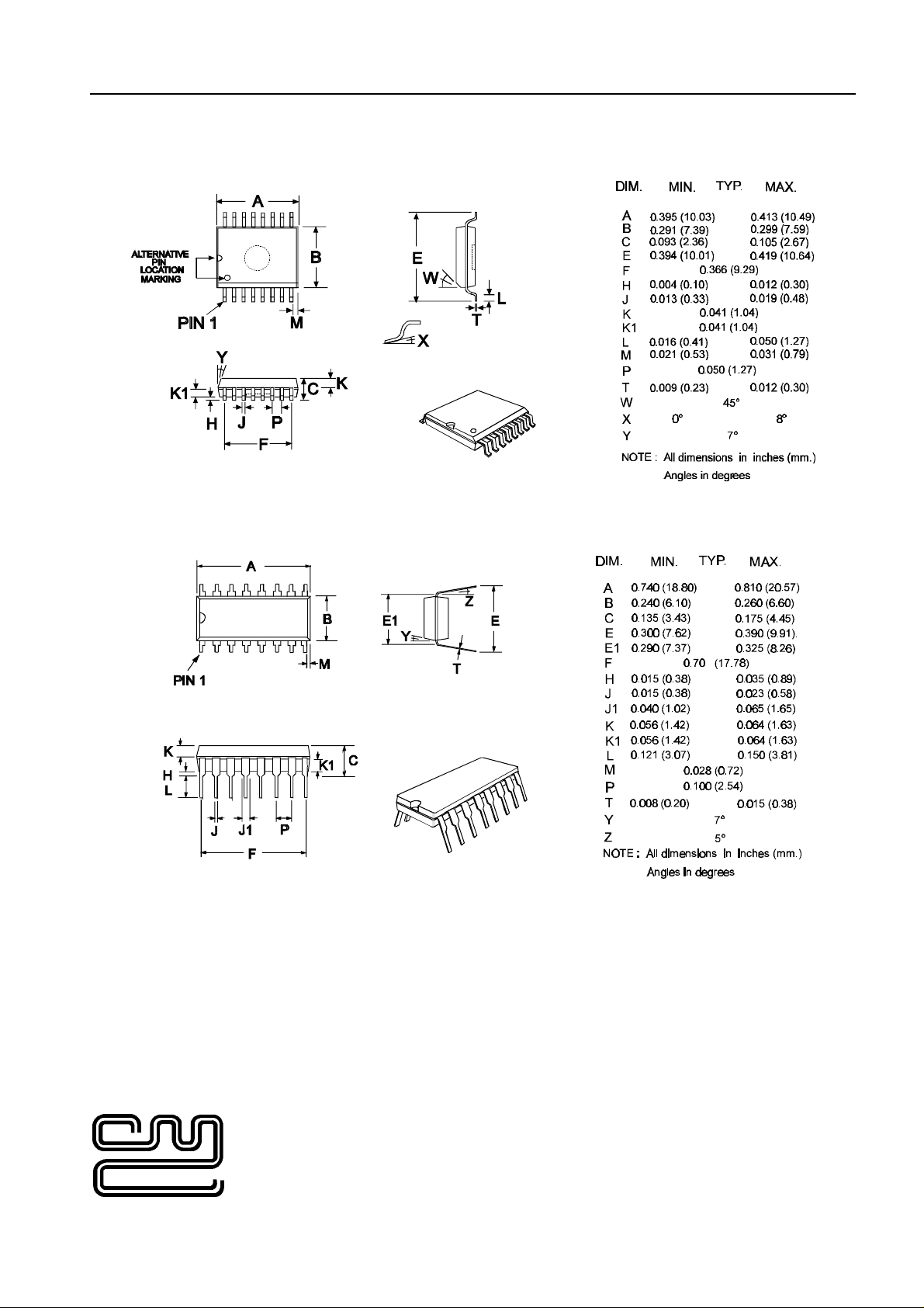
1.7.2 Packaging
Figure 9 D4 Mechanical Outline: Order as part no. FX663D4
Figure 10 P3 Mechanical Outline: Order as part no. FX663P3
Handling precautions: This product includes input protection, however, precautions should be taken to
prevent device damage from electro-static discharge. CML does not assume any responsibility for the
use of any circuitry described. No IPR or circuit patent licences are implied. CML reserves the right at
any time without notice to change the said circuitry and this product specification. CML has a policy of
testing every product shipped using calibrated test equipment to ensure compliance with this product
specification. Specific testing of all circuit parameters is not necessarily performed.
CONSUMER MICROCIRCUITS LIMITED
1 WHEATON ROAD Telephone: +44 1376 513833
WITHAM - ESSEX Telefax: +44 1376 518247
CM8 3TD - ENGLAND e-mail: sales@cmlmicro.co.uk
http://www.cmlmicro.co.uk
 Loading...