

Page 1
4.1
PRODUCT INFORMATION
FX641
Dual Subscriber Private
Metering (SPM) Detector
Selectable Tone Follower or
Packet Mode Outputs
High Speech-Band Rejection
Properties
“Output Enable” Multiplexing
Facility
Call-Charge Applications on
PABX Line Cards
+
-
+
-
Ch 2
BANDPASS
FILTER
Ch 2
INPUT
AMPLIFIER
CHANNEL 2
CHANNEL 1
Ch 2AMP OUT
Ch2 AMP IN (-)
Ch2 AMP IN (+)
Ch 2
OUTPUT
Ch 2
COMPARATOR
PULSE
GENERATOR
AND
DIVIDER
PULSE
MEASUREMENT
LOGIC
PULSE
LENGTH
LOGIC
OUTPUT
SELECT
CIRCUITS
+
-
+
-
Ch 1
BANDPASS
FILTER
XTAL/CLOCK
GENERATOR
XTAL/CLOCK
CLOCK OUT CLOCK IN
V
DD
V
BIAS
V
SS
BUFFER
CLOCK
DIVIDERS
LEVEL/
SYSTEM
SETTING
SERIAL
INPUT
LOGIC
SERIAL
DATA
SERIAL
CLOCK
PRESET LEVEL
SYSTEM SELECT
Ch 1
INPUT
AMPLIFIER
12kHz/16kHz
SYSTEM
12kHz/16kHz
SYSTEM
12kHz/16kHz
SYSTEM
TONE FOLLOWER
MODE
TONE FOLLOWER
MODE
PACKET
MODE
PACKET
MODE
INTERNAL
CLOCKS
INTERNAL
COMPARATOR
THRESHOLD
INTERNAL
COMPARATOR
THRESHOLD
GAIN
ADJUST
GAIN
ADJUST
Ch 1 AMP OUT
Ch1 AMP IN (-)
Ch1 AMP IN (+)
Ch 1
OUTPUT
OUTPUT
SELECT
Ch 1
COMPARATOR
PULSE
GENERATOR
AND
DIVIDER
PULSE
MEASUREMENT
LOGIC
PULSE
LENGTH
LOGIC
OUTPUT
SELECT
CIRCUITS
XTAL
OUTPUT
ENABLE
CHIP SELECT
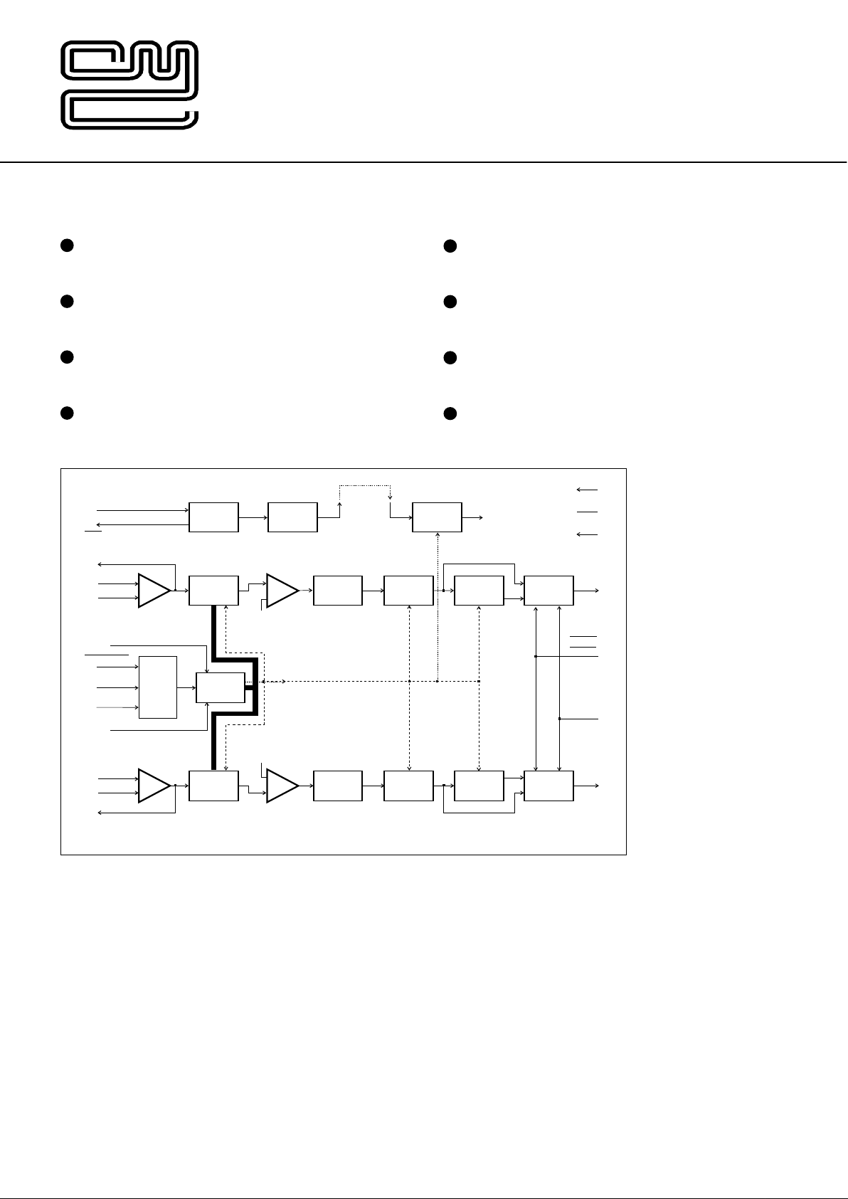
Brief Description
The FX641 is a low-power, system-selectable Dual
Subscriber Private Metering (SPM) Detector
-two
detectors on a single chip-
to indicate the presence,
on a telephone line, of either 12kHz or 16kHz
telephone call-charge frequencies.
Under µProcessor control via a common serial
interface, each channel of the FX641 will detect
call-charge pulses from a telephone line and provide a
digital output for recording, billing or security
purposes.
A common set of external components and a stable
3.579545MHz Xtal/clock input ensures that the FX641
adheres accurately to most national “Must and MustNot” decode band-edges and threshold levels.
CML Semiconductor Products
FX641
Fig.1 Functional Block Diagram
The digital output is pin-selectable to one of three
modes:
(1) Tone Follower mode -a logic level for the period of
a correct decode.
(2) Packet mode -respond/de-respond after a
cumulative period of tone or notone in a preset
period.
(3) High-impedance output -for device multiplexing.
For non-µProcessor systems a preset sensitivity/system
input allows external channel level and system setting.
This device, which is suitable for PBX and PABX
line-card and remote telephone installations, is available
in compact 24-pin plastic DIL and small outline (S.O.I.C.)
packages.
The FX641 requires approximately 4.5mA at 5-volts.
Features
Two (12kHz/16kHz) SPM
Detectors on a Single Chip
Detects 12kHz and 16kHz SPM
Frequencies
Xtal Accuracy; Stable Frequency
Limits
“Controlled” (µC) and “Fixed”
Signal Sensitivity Modes
Publication D/641/3 November 1997
Provisional Issue
Page 2

4.2
Pin Number Function
FX641
D2/P4
1
2
3
4
5
6
7
8
9
10
11
12
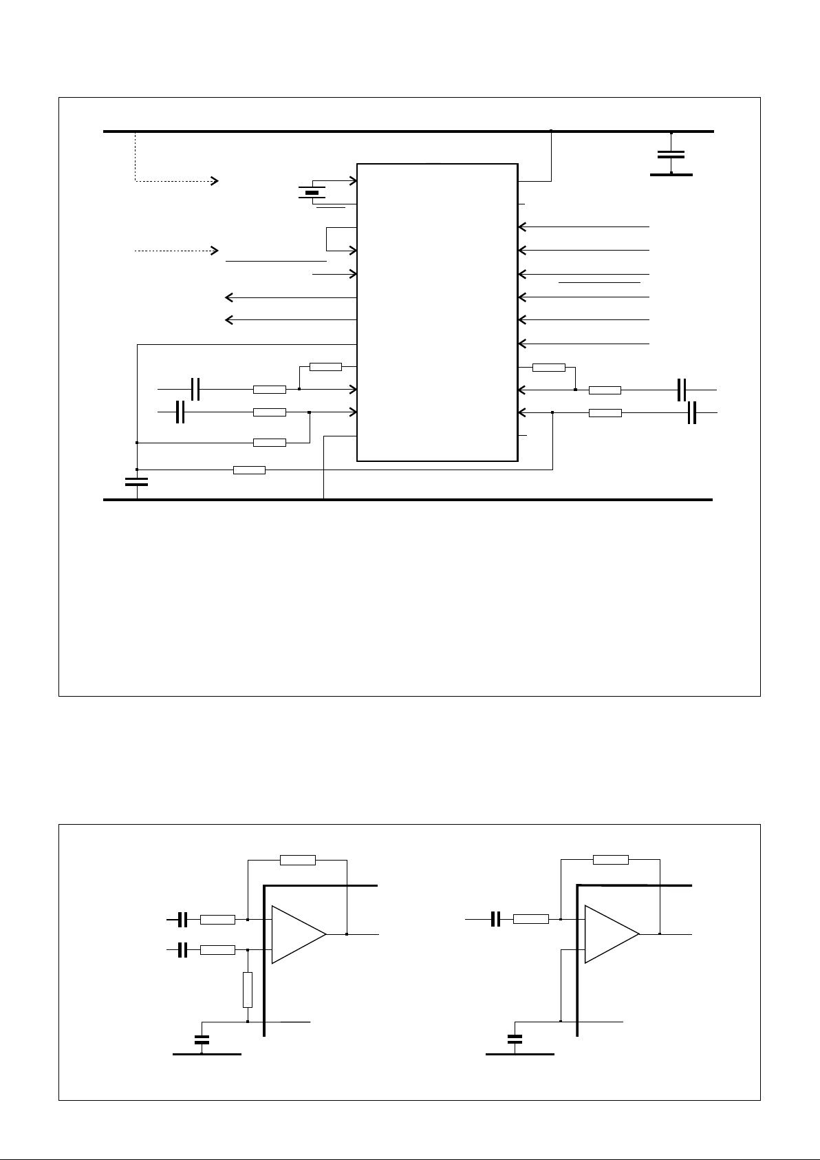
Xtal/Clock: The input to the on-chip clock oscillator; for use with a 3.579545MHz Xtal in conjunction
with the Xtal output; circuit components are on-chip. When using a Xtal input, the Clock Out pin
should be connected directly to the Clock In pin. If a clock pulse input is employed to the Clock In pin,
this (Xtal/Clock) pin must be connected directly to V
DD
(see Figure 2). See Figure 4 for details of clock
frequency distribution.
Xtal: The output of the on-chip clock oscillator inverter.
Clock Out: The buffered output of the on-chip-clock oscillator inverter. If a Xtal input is employed,
this output should be connected directly to Clock In pin. This output can support up to 3 additional
FX641 microcircuits. See Figure 4 for details of clock frequency distribution.
Clock In: The 3.579545 clock pulse input to the internal clock dividers. If an externally generated
clock pulse input is employed, the Xtal/Clock input pin should be connected to VDD.
Output Enable: For multi-chip output multiplexing; controls the state of both Ch1 and Ch2 outputs.
When this input is placed high (logic '1') both outputs are set to a high impedance. When placed low
(logic '0') both outputs are enabled.
Ch 2 Output: The digital output of the Channel 2 SPM detector when enabled. The format of the
signal at this pin, in common with Ch 1, is selectable to either 'Tone Follower' or 'Packet' mode via the
Output Select input.
Ch 1 Output: The digital output of the Channel 1 SPM detector when enabled. The format of the
signal at this pin, in common with Ch 2, is selectable to either 'Tone Follower' or 'Packet' mode via the
Output Select input.
V
BIAS
: The output of the on-chip analogue bias circuitry. Held internally at VDD/2, this pin should be
decoupled to VSS (see Figure 2).
Ch 1 Amp Out: The output of the Channel 1 Input Amplifier. See Figures 2 and 3.
Ch 1 Amp In (-): The negative input to the Channel 1 Input Amplifier. See Figures 2 and 3.
Ch 1 Amp In (+): The positive input to the Channel 1 Input Amplifier. See Figures 2 and 3.
VSS: Negative supply rail (GND).
Page 3

4.3
FX641
D2/P4
13
14
15
16
17
18
19
20
21
22
23
24
No internal connection; leave open circuit.
Ch 2 Amp In (+): The positive input to the Channel 2 Input Amplifier. See Figures 2 and 3.
Ch 2 Amp In (-): The negative input to the Channel 2 Input Amplifier. See Figures 2 and 3.
Ch 2 Amp Out: The output of the Channel 2 Input Amplier. See Figures 2 and 3.
Output Select: A logic input to set the Channel 1 and Channel 2 output modes.
When high (logic '1'), the outputs are in the Tone Follower mode; when low (logic '0'), the outputs are
in the Packet mode.
Preset Level: A logic input to set the sensitivity mode of the FX641.
When high (logic '1'), both channels are in the Fixed Sensitivity mode. The external components
govern the input sensitivity; the System Select input selects 12kHz or 16kHz operation. When low
(logic '0'), both channels are in the Controlled Sensitivity mode. Device sensitivities and system
selection are via the Chip Select/Serial Data/Serial Clock inputs. This input has an internal pullup
resistor on chip (Fixed Sensitivity Mode).
Chip Select: The Chip Select input for use in data loading when using the FX641 in the Controlled
Sensitivity mode (see Figure 9).
The device is selected when this input is set low (logic '0').
When the device is in the Fixed Sensitivity mode this input should be connected to either VSS or VDD.
Serial Clock: The Serial Clock input for use in data loading when using the FX641 in the Controlled
Sensitivity mode (see Figure 9). Data is loaded to the FX641 on this clock's rising edge.
When the device is in the Fixed Sensitivity mode this input should be connected to either VSS or VDD.
Serial Data: The Serial Data input for use in data loading when using the FX641 in the Controlled
Sensitivity mode (see Figure 9 and Table 2).
When the device is in the Fixed Sensitivity mode this input should be connected to either VSS or VDD.
System Select: In the Fixed Sensitivity mode this pin selects the system frequency.
High (logic ‘1’) = 12kHz; Low (logic ‘0’) = 16kHz.
In the Controlled Sensitivity mode this pin is inactive and may be left unconnected.
This pin has an internal pullup resistor on chip.
No internal connection; leave open circuit.
VDD: Positive supply rail; a single, stable power supply is required. Critical levels and voltages within
the FX641 are dependant upon this supply. This pin should be decoupled to VSS by a capacitor
mounted close to the pin.
Pin Number Function
Page 4
4.4
Application Information
Fig.3 Example Input Configurations
+
-
Tip (a)
Ring (b)
INPUT AMP
FX641 (par t)
FX641 (par t)
V
BIAS
V
SS
+
-
INPUT AMP
V
BIAS
V
SS
Common Mode Input
XTAL
XTAL/CLOCK
XTAL/CLOCK
For use with a Clock Pulse input
- Remove Xtal (X
1
)
- Connect Pin 1 to V
DD
- Remove link (Pins 3/4)
- Input clock pulses to CLOCK IN
See Figure 4
CLOCK IN
IN
OUT
CLOCK
Ch2 OUTPUT
Ch1 OUTPUT
Ch1 AMP IN (+)
V
BIAS
V
DD
V
DD
V
SS
V
SS
V
SS
C
1
X
1
R
3
R
1
R
2
R
4
R
8
R
6
C
6
C
5
R
5
C
3
C
4
C
2
R
7
FX641D2
1
2
3
11
12
24
23
22
21
20
19
18
17
16
15
14
13
4
5
6
7
8
9
10
OUTPUT ENABLE
Ch1 AMP OUT
Ch1 AMP IN (-)
Ch2 AMP OUT
OUTPUT SELECT
PRESET LEVEL
SERIAL CLOCK
SERIAL DATA
SYSTEM SELECT
Ch2 AMP IN (-)
Ch2 AMP IN (+)
CHIP SELECT
Component Value Tolerance
R
1
68kΩ ± 1%
R
2
68kΩ ±1%
R
3
750kΩ ±1%
R
4
750kΩ ±1%
R
5
68kΩ ± 1%
R
6
68kΩ ± 1%
R
7
750kΩ ±1%
R
8
750kΩ ±1%
C
1
1.0µF ±20%
C
2
1.0µF ±20%
C
3
270pF ±5%
C
4
270pF ±5%
C
5
270pF ±5%
C
6
270pF ±5%
X
1
3.579545MHz
Fixed Sensitivity Setting
Note that when calculating/selecting gain components, R3, R4, R7 and R8 should always be greater than or equal to
100kΩ.
Differential Input
Fig.2 Recommended External Components
Page 5

4.5
Application Information ......
µController
XTAL
XTAL/CLOCK
"OUTPUT ENABLE"
ADDRESSING
XTAL/CLOCK
XTAL/CLOCK
XTAL/CLOCK
CLOCK
OUT
V
DD
CLOCK
IN
CLOCK
IN
Ch2OUTPUT
Ch 2
Ch 2
Ch 2
Ch 2
Ch1OUTPUT
Ch 1
Ch 1
Ch 1
Ch 1
OUTPUT
ENABLE
CLOCK
IN
CLOCK
IN
X
1
FX641
(used as
Master
Oscillator)
FX641 FX641 FX641
I/O Ports
3 to’N’ LINE
DECODER
Maximum number of driven clocks (including Master) = 4
Maximum capacitive load on Clock Out output = 15.0pF
SIGNAL INPUT
TONE NOTONE
RESPONSE
DELAY
DERESPONSE
DELAY
SIGNAL INPUT ......
TONE FOLLOWER OUTPUT
Ch1 and Ch 2 OUTPUTS
PACKET MODE OUTPUT ......
TONE FOLLOWER OUTPUT ......
PACKET MODE OUTPUT
Fig.5 Tone Follower and Packet Mode Outputs
Xtal/Clock Distribution
The FX641 requires a 3.579545MHz Xtal or clock
pulse input. With the exception of the Xtal, all oscillator
components are incorporated on chip. If a Xtal input is
employed the Clock Out pin should be directly linked to
the Clock In pin.
To reduce component and layout complexity, the
clock requirements of up to 3 additional FX641
microcircuits may be supplied from a Xtal-driven
FX641 acting as the system master clock. With
reference to Figure 4, the clock should be distributed
as illustrated and the Xtal/Clock pins of the driven
microcircuits should be connected directly to V
DD.
Note that the maximum load on the master Clock Out
pin should not be exceeded.
Channel Outputs
Channels 1 and 2 outputs operate together under
the control of the Output Enable and Output Select
inputs. Table 3 describes the operations.
The Front Page description describes the output
formats.
Fig.4 Examples of Xtal/Clock Distribution and Output Multiplexing
Page 6

4.6
Application Information ......
Sensitivity Setting
To enable the FX641 to operate correctly to most national 12kHz and 16kHz SPM specifications, the input
sensitivity can be accurately adjusted and set.
There are two different pin-selectable modes of sensitivity setting available to the FX641: Controlled Sensitivity
Mode and Fixed Sensitivity Mode
The Controlled Sensitivity mode allows the sensitivity setting from a µController via a 6-bit serial data input. This
same serial input also sets operation (bit 0) to either 12kHz or 16kHz systems. Both channels are set identically.
The Fixed Sensitivity mode allows the sensitivity of each channel to be set to a fixed “gain” by external
components at the input amplifiers. Operation to either 12kHz or 16kHz is by the System Select input.
Controlled Sensitivity Setting
The figures provided in Table 2 assume:
1. The recommended amplifier components (see Figure 2) are employed providing an amplifier gain at
16kHz of 19.8dB ±0.3dB or at 12kHz of 19.1dB ±0.3dB.
2. A comparator sensitivity of 1.6dB(ref.) ±1dB (the variation being due to filter gain error, filter output offset,
comparator input offset or a combination of all 3).
3. The applied VDD is 5.0 volts; 0dB (ref.) = 775mVrms.
12kHz System 16kHz System
Bit D0 = ‘1’ Bit D0 = ‘0’
Serial Data Bandpass Minimum Nominal Maximum Minimum Nominal Maximum
Bits Filter Gain Sensitivity Sensitivity Sensitivity Sensitivity Sensitivity Sensitivity
D5 - D
1
(dB) dB(ref.) dB(ref.) dB(ref.) dB(ref.) dB(ref.) dB(ref.)
0 0 0 0 0 0 -16.2 -17.5 -18.8 -16.9 -18.2 -19.5
0 0 0 0 1 1.0 -17.2 -18.5 -19.8 -17.9 -19.2 -20.5
0 0 0 1 0 2.0 -18.2 -19.5 -20.8 -18.9 -20.2 -21.5
0 0 0 1 1 3.0 -19.2 -20.5 -21.8 -19.9 -21.2 -22.5
0 0 1 0 0 4.0 -20.2 -21.5 -22.8 -20.9 -22.2 -23.5
0 0 1 0 1 5.0 -21.2 -22.5 -23.8 -21.9 -23.2 -24.5
0 0 1 1 0 6.0 -22.2 -23.5 -24.8 -22.9 -24.2 -25.5
0 0 1 1 1 7.0 -23.2 -24.5 -25.8 -23.9 -25.2 -26.5
0 1 0 0 0 8.0 -24.2 -25.5 -26.8 -24.9 -26.2 -27.5
0 1 0 0 1 9.0 -25.2 -26.5 -27.8 -25.9 -27.2 -28.5
0 1 0 1 0 10.0 -26.2 -27.5 -28.8 -26.9 -28.2 -29.5
0 1 0 1 1 11.0 -27.2 -28.5 -29.8 -27.9 -29.2 -30.5
0 1 1 0 0 12.0 -28.2 -29.5 -30.8 -28.9 -30.2 -31.5
0 1 1 0 1 13.0 -29.2 -30.5 -31.8 -29.9 -31.2 -32.5
0 1 1 1 0 14.0 -30.2 -31.5 -32.8 -30.9 -32.2 -33.5
0 1 1 1 1 15.0 -31.2 -32.5 -33.8 -31.9 -33.2 -34.5
1 0 0 0 0 16.0 -32.2 -33.5 -34.8 -32.9 -34.2 -35.5
1 0 0 0 1 17.0 -33.2 -34.5 -35.8 -33.9 -35.2 -36.5
1 0 0 1 0 18.0 -34.2 -35.5 -36.8 -34.9 -36.2 -37.5
1 0 0 1 1 19.0 -35.2 -36.5 -37.8 -35.9 -37.2 -38.5
1 0 1 0 0 20.0 -36.2 -37.5 -38.8 -36.9 -38.2 -39.5
1 0 1 0 1 21.0 -37.2 -38.5 -39.8 -37.9 -39.2 -40.5
1 0 1 1 0 22.0 -38.2 -39.5 -40.8 -38.9 -40.2 -41.5
1 0 1 1 1 23.0 -39.2 -40.5 -41.8 -39.9 -41.2 -42.5
1 1 0 0 0 24.0 -40.2 -41.5 -42.8 -40.9 -42.2 -43.5
1 1 0 0 1 25.0 -41.2 -42.5 -43.8 -41.9 -43.2 -44.5
1 1 0 1 0 26.0 -42.2 -43.5 -44.8 -42.9 -44.2 -45.5
1 1 0 1 1 27.0 -43.2 -44.5 -45.8 -43.9 -45.2 -46.5
11100
11101
11110
11111
Table 2 Controlled Sensitivity Setting Information
These states should never be used. If senstivities of this order are required (eg. the Swedish Rural SPM
Specification), it is recommended that the Controlled Sensitivity setting is set to 20dB (1 0 1 0 0) and
external components selected to set the Input Amp gain to a higher figure.
Page 7

4.7
Application Information ......
Controlled Sensitivity Setting ......
With the external gain (sensitivity) components employed as shown in Figure 2 the gain of the input stages is
19.8dB (12kHz) or 20.5dB (16kHz). For controlled sensitivity setting the gain of each bandpass filter, and hence
the device sensitivity, is adjusted by the applied serial bits D1 to D5.
In the Controlled Sensitivity mode the system frequency is selected by bit D0 (‘1’ = 12kHz; ‘0’ = 16kHz). Data is
loaded Bit 5 (D5) first.
Table 2 details the serial data input to produce the required sensitivity. Minimum, Nominal and Maximum
Sensitivity figures are provided to make complete allowance for internal circuit offsets and component tolerances.
0dB(ref.) = 775mVrms at VDD = 5.0 volts; varies directly with VDD.
Examples are provided as a guide to meeting national specifications.
MUST DECODE
-21dB(ref.)
-27dB(ref.)
MUST-NOT DECODE
WILL DECODE
WILL-NOT DECODE
-21.9
-23.2 5.0dB
-24.5
-22.9
-24.2 6.0dB
-25.5
-23.9
-25.2 7.0dB
-26.5
German FTZ Specification 16kHz
This system has a Must Decode level of -21dB(ref.)
and a Must-Not Decode level of -27dB(ref.). Reference
to Table 2 shows that Bandpass Filter Gain settings of
5dB, 6dB or 7dB will enable an FX641 channel to meet
this level specification.
Figure 6 illustrates the range of these various settings.
Hence to meet the German FTZ specification, the
input data (D5 to D0 ) can be:
0 0 1 0 1 0 5.0dB
or
0 0 1 1 0 0 6.0dB
or 0 0 1 1 1 0 7.0dB
Selecting the middle setting would give the greatest
noise immunity.
System Preset Output Output
Select Level Select Enable Operating Mode
X 0 0 0 Packet Mode Output; Serial Data Control
X 0 1 0 Tone Follower Output; Serial Data Control
0 1 0 0 Packet Mode Output; Preset Sensitivity 16kHz
1 1 0 0 Packet Mode Output; Preset Sensitivity 12kHz
0 1 1 0 Tone Follower Output; Preset Sensitivity 16kHz
1 1 1 0 Tone Follower Output; Preset Sensitivity 12kHz
X X X 1 Tristate Output High Z
Table 3 Operating Mode Configurations X = don't care
Fig.6 German Specification -Possible Settings
MUST DECODE
WILL DECODE
WILL-NOT DECODE
-17.36dB(ref.)
-23.8dB(ref.)
MUST-NOT DECODE
-18.2
-19.5 2.0dB
-20.8
-19.2
-20.5 3.0dB
-21.8
-20.2
-21.5 4.0dB
-22.8
Fig.7 French Specification -Possible Settings
French Specification 12kHz
This system has a Must Decode level of
-17.36dB(ref.) and a Must-Not Decode level of
-23.8dB(ref.). Reference to Table 2 shows that
Bandpass Filter Gain settings of 2dB, 3dB or 4dB will
enable an FX641 channel to meet this level
specification.
Fig 7 illustrates the range of these various settings.
Hence to meet the French SPM specification, the
input data (D5 to D0 ) can be:
0 0 0 1 0 1 2.0dB
or
0 0 0 1 1 1 3.0dB
or 0 0 1 0 0 1 4.0dB
Selecting the middle setting would give the greatest
noise immunity.
Page 8

4.8
Application Information ......
Application Information ......
SIGNAL LEVEL (dB): 0dB ref = 775mVrms
AMPLIFIER GAIN (dB)
MUST DECODE LEVEL
MINIMUM AMPLIFIER GAIN MAXIMUM AMPLIFIER GAIN
MUST-NOT DECODE LEVEL
VDD= 5.0 (+/- 0.1) VOLTS; TEMP = -40oC to +85oC
-50
-45
-40
-35
-30
-25
-20
-15
-10
-20 -15 -10 -5 0 5 10 15 20 25
Fig.8 Input Gain Calculation Graph for use in the Fixed Sensitivity Mode
Page 9

4.9
Application Information ......
Fixed Sensitivity Setting
In this mode the sensitivity of each channel is set
by the correct selection of the components around the
Channel Input Amplifier.
Note that the device sensitivity is directly proportional
to the applied power supply (VDD).
Input Gain Calculation
The input amplifier, with its external circuitry, is
available to set the sensitivity of the FX641 to conform
to the user's national level specification with regard to
‘Must’ and ‘Must-Not’ decode signal levels.
With reference to the graph in Figure 8, the
following steps will assist in the determination of the
required gain/attenuation.
Step 1
Draw two horizontal lines from the Y-axis (Signal
Level (dB)).
The upper line will represent the required ‘Must’
decode level.
The lower line will represent the required ‘Must-Not’
decode level.
Step 2
Mark the intersection of the upper horizontal line
and the upper sloping line; drop a vertical line from
this point to the X-axis (Amplifier Gain (dB)).
The point where the vertical line meets the X-axis
will indicate the MINIMUM Input Amp gain required
for reliable decoding of valid signals.
Step 3
Mark the intersection of the lower horizontal line
and the lower sloping line; drop a vertical line from
this point to the X-axis.
The point where the vertical line meets the X-axis
will indicate the MAXIMUM allowable Input Amp
gain.
Input signals at or below the ‘Must-Not’ decode
level will not be detected as long as the amplifier
gain is no higher than this level.
Select the
Input Gain Components
as described.
Input Gain Components
With reference to the gain components shown in
Figure 2.
The user should calculate and select external
components (R1/R3/C3, R2/R4/C4 and R5/R7/C5, R6/R8/C6)
to provide amplifier gains within the limits obtained in
Steps 2 and 3.
Component tolerances should not move the gainfigure outside these limits. The graph in Figure 8 is for the
calculation of input gain components for an FX641 using
a VDD of 5.0 (±0.1) volts.
It is recommended that the designed gain is near the
centre of the calculated range.
Microcircuit Protection Against High Voltages
Telephone systems may have high d.c. and a.c.
voltages present on the line. If the FX641 is part of a
host equipment that has its own signal input protection
circuitry, there will be no need for further protection as
long as the voltage on any pin is limited to within V
DD
+0.3V and V
SS
-0.3V.
If the host system does not have input protection, or
there are signals present outside the device's specified
limits, the FX641 will require protection diodes at its
signal inputs (+ and -). The breakdown voltage of
capacitors and the peak inverse voltage of the diodes
must be sufficient to withstand the sum of the d.c.
voltages plus all expected signal peaks.
Aliasing
Due to the switched-capacitor filters employed in
the FX641, care should be taken, with the chosen
external components, to avoid the effects of alias
distortion.
Possible Alias Frequencies:
12kHz Mode = 52kHz
16kHz Mode = 69kHz
If these alias frequencies are liable to cause
problems and/or interference, it is recommended that
anti-alias capacitors are employed across input
resistors R3 and R4 or R7 and R8.
Values of anti-alias capacitors should be chosen so
as to provide a highpass cutoff frequency, in
conjunction with R3 (R4) (R7) (R8) of approximately
20kHz to 25kHz (12kHz system) or 25kHz to 30kHz
(16kHz system).
i.e. C = 1
2 x π x f0 x R
3
When anti-alias capacitors are used, allowance
must be made for reduced gain at the SPM frequency
(12kHz or 16kHz).
Page 10

4.10
Specification
Absolute Maximum Ratings
Exceeding the maximum rating can result in device damage. Operation of the device outside the operating limits is not
implied.
Supply voltage -0.3 to 7.0V
Input voltage at any pin (ref V
SS
= 0V) -0.3 to (V
DD
+ 0.3V)
Sink/source current (supply pins) +/- 30mA
(other pins) +/- 20mA
Total device dissipation @ T
AMB
25°C 800mW Max.
Derating 10mW/°C
Operating Temperature (T
OP
): FX641D2/P4 -40°C to +85°C
Storage Temperature range (T
ST
): FX641D2/P4 -40°C to +85°C
Operating Limits
Correct operation of the device outside these limits is not implied.
Parameter Min. Max. Unit
Supply Voltage (VDD) 4.5 5.5 V
Operating Temperature (TOP) -40.0 +85.0 °C
Xtal/Clock/Clock In Frequency 3.558918 3.589368 MHz
Operating Characteristics
All device characteristics are measured under the following conditions unless otherwise specified:
V
DD
= 5.0V T
AMB
= -40°C to +85°C. Audio Level 0dB(ref.): = 775mVrms. Noise Bandwidth = 50kHz.
Xtal/Clock or ‘Clock In’ Frequency = 3.579545MHz. System Setting = 12kHz or 16kHz.
Characteristics See Note Min. Typ. Max. Unit
Supply Current - 2.0 5.0 m A
Input/Output Parameters
Clock Out Load - - 15.0 pF
Logic Inputs
Input Logic ‘1’ (High) 3. 5 - - V
Input Logic ‘0’ (Low) - - 1.5 V
Input Leakage Current (VIN = 0 to VDD) 13 -5.0 - 5.0 µA
Input Current (VIN = 0) 14 -15.0 - - µA
Channel Outputs
Output Logic ‘1’ (IOH) = 120µA) (Enabled) 1 4.6 - - V
Output Logic ‘0’ (IOL) = 360µA) (Enabled) 1 - - 0.4 V
Output Leakage Current (High-Z Output) 2 -5.0 - 5.0 µA
Input Amplifier
D. C. Gain 60.0 - - dB
Bandwidth (-3dB) - 100 - Hz
Input Impedance 1.0 - - MΩ
Overall Performance
12kHz Detect Bandwidth 3 11.82 12.18 kHz
12kHz Not-Detect Frequencies (below 12kHz) 3 - - 11.52 kHz
12kHz Not-Detect Frequencies (above 12kHz 3 12.48 - - kHz
16kHz Detect Bandwidth 3 15.76 16.24 kHz
16kHz Not-Detect Frequencies (below 16kHz) 3 - - 15.36 kHz
16kHz Not-Detect Frequencies (above 16kHz) 3 16.64 - - kHz
Level Sensitivity
Controlled Sensitivity Mode 3, 4, 12, 15 2.6 1.6 0.6 dB(ref.)
Preset Sensitivity Mode 3, 4, 5, 16 -25.4 -26.4 -27.4 dB(ref.)
Signal Quality Requirements for Correct Operation
Signal-to-Noise (Amp Input) 4, 8, 9, 10 22.0 20.0 - dB
Signal-to-Voice (Amp Input) 4, 8, 9, 11 -36.0 -40.0 - dB
Signal-to-Voice (Amp Output) 4, 8, 10, 11 -1.0 - -27.0 dB
Continued on next page ......
Page 11

4.11
Specification ......
SERIAL CLOCK
SERIAL DATA
CHIP SELECT
t
CSE
t
CYC
t
PWH
t
PWL
t
DH
t
DS
BIT D
5
BIT D
4
BIT D
0
D
3
t
CSH
Don’t
Care
Data
Fig.9 Data Load Timing for the Controlled Sensitivity Mode
Characteristics See Note Min. Typ. Max. Unit
Channel Outputs (Ch1 and Ch2) Figure 5
Mode Change Time 6 - - 500 ns
Tone Follower Mode (Table 3)
Response and De-Response Time 3, 4, 7 - - 10.0 ms
Packet Mode (Table 3)
Response and De-Response Time 3, 4, 7 40.0 - 48.0 ms
Notes
1. Tone Follower or Packet mode enabled; see Table 3.
2. Tristate selected; see Table 3.
3. With adherence to Signal-to-Voice and Signal-to Noise specifications.
4. 12kHz and/or 16kHz system.
5. With Input Amp gain setting = 0dB.
6. Time taken to change between any two of the operational modes: Tone Follower, Packet or Tristate, and with
a maximum capacitive load of 30pF on an output.
7. The time delay, after a valid serial data load (or after device powerup), before the condition of the outputs can
be guaranteed correct.
8. Immunity to false responses and/or de-responses.
9. Common Mode SPM and balanced voice input signal.
10. With SPM and voice signal amplitudes balanced; to avoid false de-responses due to saturation, the peak-topeak voice + noise level at the output of the Input Amp should be no greater than the dynamic range of the
device. For this reason, the signal-to-voice figure at the Am[ Output will vary with the sensitivity setting. The
lowest signal-to-voice figure occurs at the highest sensitivity setting (
Table 2,
27dB).
11. Maximum voice frequencies = 3.4kHz.
12. With the Input Amplifier gain at 0dB and the Bandpass Filter gain set at 0dB (Table 2); subtract 1.0dB from this
specification for each extra single dB of Bandpass Filter gain programmed.
Alternatively, with the input components as recommended in Figure 2, the sensitivity is as defined in Table 2.
13. Logic inputs with no internal pullup; Chip Select, Serial Data, Serial Clock, Output Enable, Output Select and
Clock In pins.
14. Logic inputs with an internal pullup; Preset Level and System Select pins.
15. Preset Level= ‘0’, System Select = don't care; Chip Select, Serial Clock and Serial Data inputs active;
see Table 3.
16. Preset Level = ‘1’, System Select = input active; Chip Select, Serial Clock and Serial Data inputs inactive;
see Table 3.
Parameter Min. Typ. Max. Unit
t
PWH
Serial Clock ‘High’ Pulse Width 250 - - ns
t
PWL
Serial Clock ‘Low’ Pulse Width 250 - - ns
t
CYC
Serial Clock Period 600 - - ns
t
CSE
Chip Select ‘Low’ to Clock ‘High’ Edge 450 - - ns
t
DH
Data Hold Time 50.0 - - ns
t
DS
Data Setup Time 250 - - ns
t
CSH
Chip Select ‘High’ from:
Clock ‘High’ Edge 50.0 - - ns
Clock ‘High’ Edge - - 1 serial clock period
Page 12

4.12
CML does not assume any responsibility for the use of any circuitry described. No circuit patent licences are implied
and CML reserves the right at any time without notice to change the said circuitry.
FX641D2 24-pin plastic S.O.I.C.
Ordering Information
FX641D2 24-pin plastic S.O.I.C.
FX641P4 24-pin plastic DIL
NOT TO SCALE
Max. Body Length 15.70mm
Max. Body Width 7.65mm
NOT TO SCALE
Max. Body Length 31.85mm
Max. Body Width 13.82mm
Package Outlines
The FX641 is available in the package styles outlined
below. Mechanical package diagrams and
specifications are detailed in Section 10 of this
document.
Pin 1 identification marking is shown on the relevant
diagram and pins on all package styles number
anti-clockwise when viewed from the top.
Handling Precautions
The FX641 is a CMOS LSI circuit which includes input
protection. However precautions should be taken to
prevent static discharges which may cause damage.
FX641P4 24-pin plastic DIL
 Loading...