

Page 1
CML Semiconductor Products
PRODUCT INFORMATION
FX631
Features
Detects 12kHz and 16kHz SPM
Frequencies
Low Power (3.0 Volt
Operation
High Speechband Rejection
Properties
XTAL/CLOCK
XTAL/CLOCK
OSCILLATOR
XTAL
<1.0mA)
MIN
CLOCK
OUT
Low-Voltage SPM Detector
Publication D/631/6 June 1997
Tone-Follower and P ac ket Mode
Outputs
Applications
Complex and/or Simple
T elephone Systems
Call-Charge/-Logging
Systems
CLOCK IN
SYSTEM
CLOCK
DIVIDERS
V
SS
V
DD
SYSTEM
(12kHz/16kHz)
SIGNAL
IN (-)
SIGNAL
IN (+)
AMP OUT
V
BIAS
INPUT AMP
-
+
12kHz/16kHz
+20dB
LEVEL DETECTOR
1
DIVIDER
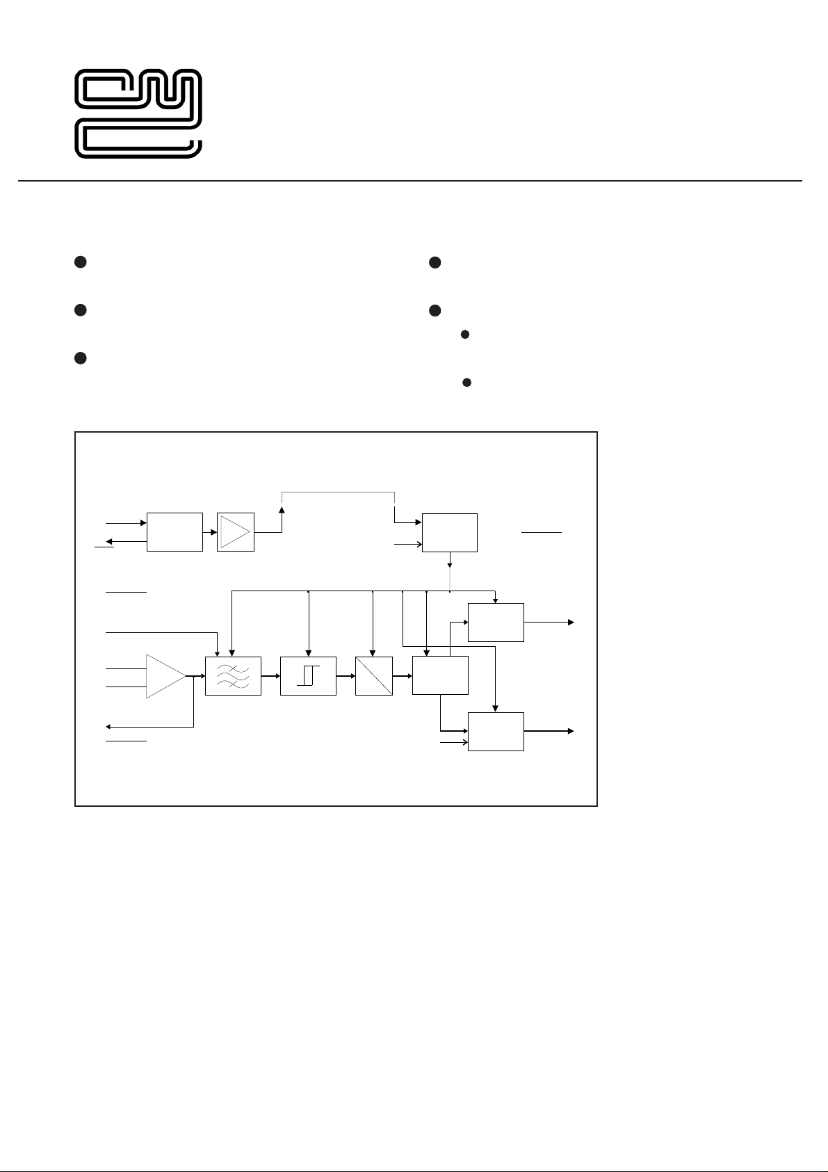
Fig.1 Functional Block Diagram
Brief Description
The FX631 is a low-power, system-selectable
Subscriber Pulse Metering (SPM) detector to indicate
the presence, on a telephone line, of both 12kHz and
16kHz telephone call-charge frequencies.
Deriving its input directly from the telephone line,
input amplitude/sensitivities are component adjustable
to the user's national ‘Must/Must-Not Decode’
specifications via an on-chip input amplifier, whilst the
12kHz and 16kHz frequency limits are accurately
defined by the use of an external 3.579545MHz
telephone-system Xtal or clock-pulse input.
The FX631, which demonstrates high 12kHz and
16kHz performance in the presence of both voice and
noise, can operate from either a single or differential
analogue signal input from which it will produce two
individual logic outputs.
32
TONE FOLLOWER
OUTPUT
PACKET MODE
OUTPUT
FX631
MEASURE
SYSTEM
PERIOD
TONE
FOLL OW ER
LOGIC
PACKET
TONE
LOGIC
1. Tone Follower Output - A 'tone-following' logic
output producing a “Low” level for the period of a
correct decode and a “High” level for a bad
decode or N
OTONE.
2. Packet (Cumulative Tone) Mode Output - To
respond and de-respond after a cumulative 40ms
of good tone (or N
OTONE) in any 48ms period.
This process will ignore small fluctuations or
fades of a valid frequency input and is available
for µProcessor ‘Wake-Up’, Minimum tone
detection, N
OTONE indication or transient
avoidance.
This system (12kHz/16kHz) selectable microcircuit,
which may be line-powered, is available in 16-pin plastic
DIL and surface mount SOIC and 24-pin plastic SSOP
packages.
1
Page 2

Pin Number Function
FX631
D5
1
4
5
6
8
12
FX631
DW/P
1
2
3
4
7
8
Xtal/Clock: The input to the on-chip clock oscillator; for use with a 3.579545MHz Xtal in
conjunction with the Xtal output (see Figure 2); circuit components are on chip. Using this
mode of clock operation, the Clock Out pin should be connected directly to the Clock In pin. If
2.3 Pin Function Description
a clock pulse input is employed to the Clock In pin, this pin must be connected directly to V
(see Figure 2).
XTAL The input of the oscillator inverter.
XTALN The output of the oscillator inverter
Xtal: The output of the on-chip clock oscillator inverter.
CLKIN The input to the internal clock divider circuitry.
When a 3.579545MHz crystal is used, it should be connected across XTAL &
Clock Out: The buffered output of the on-chip clock oscillator inverter. If a Xtal input is
should be directly connected to CLKIN. No other external components are necessary because
employed this output should be connected directly to the Clock In pin.
the other oscillator components (capacitor, resistor) are on chip.
When an externally available clock signal is used, it should be inserted at CLKIN. XTAL should
be tied to VDD or Vss and
Clock In: The 3.579545MHz clock pulse input to the internal clock-dividers. If a clock pulse
XTAL should be left open circuit.
input is employed, the Xtal/Clock input (Pin 1) should be connected to V
SYSTEM A logic input pin which controls whether the device detects 12Khz SPM tones (logic 1)
or 16Khz SPM tones (logic 0). It has an internal 1 Mohm pull- up resistor (l 2Khz).
V
: The output of the on-chip analogue bias circuitry. Held internally at VDD/2, this pin should
BIAS
NEGIP The negative input, positive input and output respectively of the gain adjusting POSIP
be decoupled to V
amplifier.
V
: Negative supply rail (GND).
External components are used in conjunction with the op -amp according to the required level
SS
sensitivity and depending on whether the incoming signal is differential or common mode.
SS
AMPOP
(see Figure 2).
XTAL and XTAL
. See Figure 2.
DD
DD
13
17
18
19
20
21
24
10
11
13
14
15
16
9
Signal In (+):
Signal In (-):
The positive and negative signal inputs to, and the output from, the input gain
VDD The power supply, ground and filter bias pins respectively.
adjusting signal amplifier. Refer to the graph in Figure 4 for guidance on
VSS
setting level sensitivities to national specifications, and the selection of gain
BIAS Voo and bias should each be de- coupled, via a 1 .0@F capacitor, to VSS.
adjusting components.
Amp Out:
Tone Follower Output: This output provides a logic “0” (Low) for the period of a detected
tone, and a logic “1” (High) for N
TTFOP TRUE TONE FOLLOWER OUTPUT. This is the pin that responds and de-
responds within 4ms of a good tone appearing or disappearing.
It is thus like an envelope of the SPM tone.
· logic 0 represents ‘detect’ and logic 1 represents ‘not detect’.
OTONE detection. See Figure 7.
Packet Mode Output: A logic output that will be available after a cumulation of 40ms of 'good'
tone has been received. This packet mode tone follower will only respond when a tone
DTFOP This is the output of the ‘delayed tone follower’ block.
frequency of sufficient quality has been received for sufficient time, i.e. a cumulation of 40ms in
any 48ms, short tone bursts or breaks will be ignored. This output provides a logic “0” (Low)
It will respond when 40ms of good tone has been received within any 48ms window. The 48ms
is divided into 24 ‘packets’ of 2ms each (16Khz mode) or 15 ‘packets’ of 2.667ms each (12Khz
for a detected tone and a logic “1” (High) for N
mode). Each packet represents 32 cycles of SPM frequency. The window is a shifting window,
ie. the 48ms window is assessed every 2ms (16Khz mode) or 2.667ms (12Khz). If the
System: The logic input to select device operation to either 12kHz (logic “1” - High) or 16kHz
necessary number of good packets are consecutive, the output will respond in the minimum
(logic “0” - Low) SPM systems. This input has an internal 1MΩ pullup resistor (12kHz).
time of 40ms.
V
: Positive supply rail. A single, stable power supply is required. Critical levels and voltages
DD
· logic 0 represents ‘detect’ and logic 1 represents ‘not detect’.
OTONE detection. See Figure 7.
within the FX631 are dependant upon this supply. This pin should be decoupled to V
by a capacitor mounted close to the pin.
Note that if this device is ‘line’ powered, the resulting supply must be stable. See notes on
Microcircuit Protection from high and spurious line voltages.
SS
2, 3,
7, 9,
10, 11,
14,
15, 16,
22, 23
5, 6,
12
No internal connection, leave open circuit.
2
Page 3
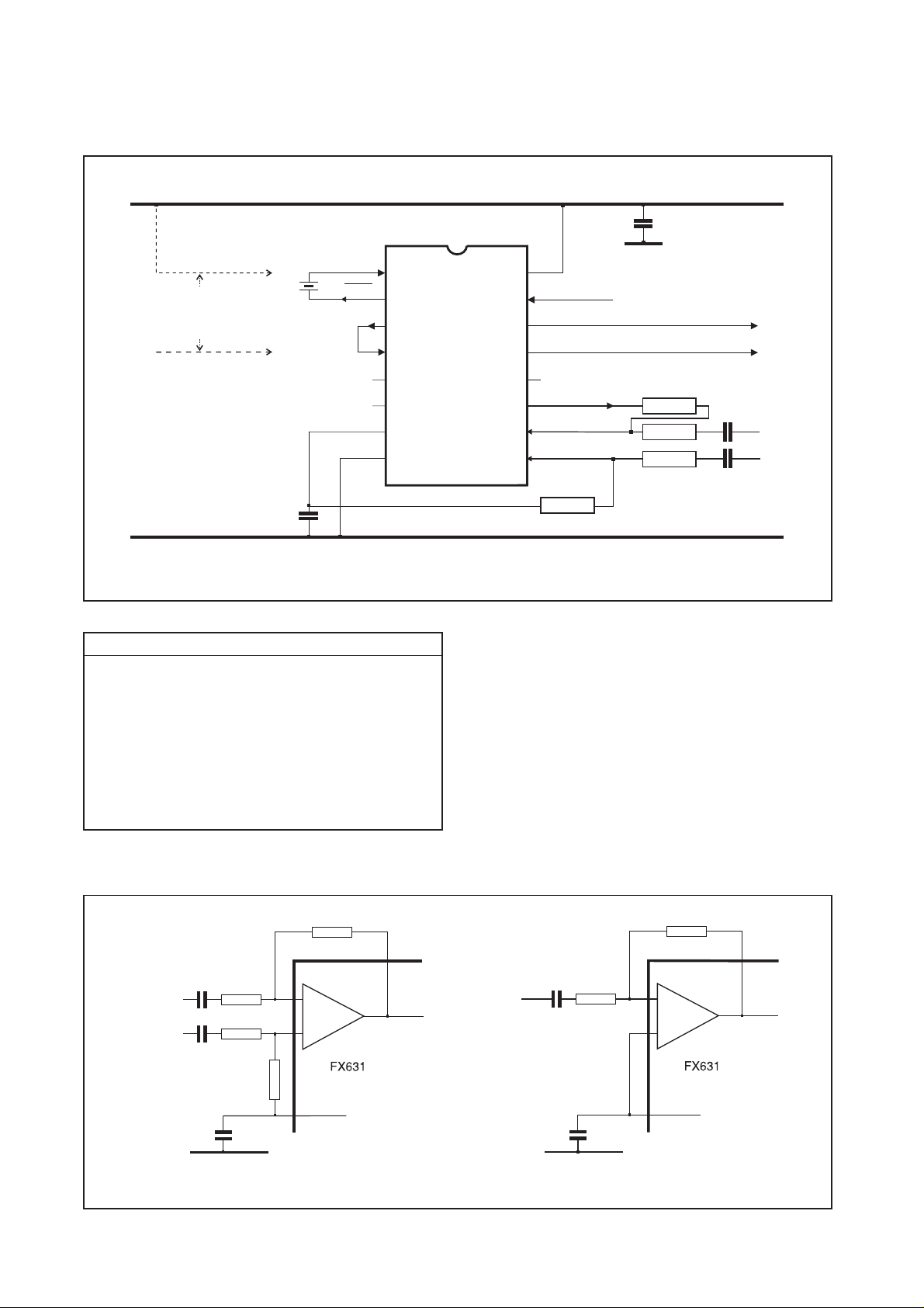
Application Information
External Components
XTAL/CLOCK
X
For use with a Clock Pulse input
- Remove Xtal (X
- Connect Pin 1 to V
- Remove link (Pins 3/4)
- Input clock pulses to CLOCK IN
CLOCK IN
)
1
DD
1
CLOCK OUT
C
2
XTAL/CLOCK
XTAL
CLOCK IN
V
BIAS
V
V
DD
C
1
V
V
1
2
3
4
FX631DW
5
6
7
SS
8
V
16
15
14
13
12
11
10
9
SS
DD
SYSTEM
PACKET MODE OUTPUT
TONE FOLLOWER OUTPUT
AMP OUT
SIGNAL IN (-)
SIGNAL IN (+)
R
4
SS
R
1
C
3
R
2
C
R
3
4
Fig.2 Recommended External Components - Differential Input Mode
Component Value
R
1
R
2
R
3
R
4
C
1
C
2
C
3
C
4
X
1
R
FEEDBACK
R
IN (-)
R
IN (+)
R
BIAS
1.0µF ±20%
1.0µF ±20%
C
IN (-)
C
IN (+)
3.579545MHz
External Components
1. The values of the Input Amp gain components
illustrated are calculated using the Input Gain
Calculation Graphs (Figures 4 and 5).
Whilst calculating input gain components, for
correct operation, it is recommended that the
values of resistors R
than, or equal to, 33kΩ.
2. Refer to following pages for advice on Microcircuit
Protection from high and spurious line voltages.
Differential Input Common Mode Input
INPUT AMP
Tip (a)
Ring (b)
-
+
and R4 are always greater
1
INPUT AMP
-
+
V
BIAS
V
SS
Fig.3 Example Input Configurations
V
BIAS
V
SS
3
Page 4

Application Information ......
-10
-15
-20
MUST DECODE LEVEL
-25
MUST NOT DECODE LEVEL
-30
-35
-40
-45
SIGNAL LEVEL (dB) 0dB ref: 775mVrms
-50
-25 -20 -15 -10 -5 0 5 10 15 20 25
Fig.4 Input Gain Calculation Graph for VDD = 3.3V
MINIMUM AMPLIFIER GAIN MAXIMUM AMPLIFIER GAIN
AMPLIFIER GAIN (dB)
VDD=3.3(+/-0.1)VOLTS TEMP= -40oCto+85oC
Fig.5 Input Gain Calculation Graph for VDD = 5.0V
o
4
o
Page 5

Application Information ......
Input Gain Calculation
The input amplifier, with its external circuitry, is
provided on-chip to set the sensitivity of the FX631 to
conform to the user's national level specification with
regard to ‘Must’ and ‘Must-Not’ decode signal levels.
With reference to the graphs in Figures 4 and 5,
the following steps will assist in the determination of
the required gain/attenuation.
Step 1
Draw two horizontal lines from the Y-axis (Signal
Levels (dB)).
The upper line will represent the required ‘Must’
decode level.
The lower line will represent the required ‘MustNot’ decode level.
Step 2
Mark the intersection of the upper horizontal line
and the upper sloping line; drop a vertical line
from this point to the X-axis (Amplifier Gain (dB)).
The point where the vertical line meets the X-axis
will indicate the MINIMUM Input Amp gain
required for reliable decoding of valid signals.
Step 3
Mark the intersection of the lower horizontal line
and the lower sloping line; drop a vertical line from
this point to the X-axis.
The point where the vertical line meets the X-axis
will indicate the MAXIMUM allowable Input Amp
gain.
Input signals at or below the ‘Must-Not’ decode
level will not be detected as long as the amplifier
gain is no higher than this level.
Select the gain components as described
opposite.
Input Gain Components
With reference to the gain components shown in Figures
2 and 3.
The user should calculate and select external
components (R
gain within the limits obtained in Steps 2 and 3.
Component tolerances should not move the gain-figure
outside these limits.
It is recommended that the designed gain is near the
centre of the calculated range. The graphs in Figures 4 and
5 are for the calculation of input gain components for an
FX631 using a V
respectively.
, R2/C3, R3/C4, R4) to provide an amplifier
1
of 3.3 (±0.1) or 5.0 (±0.5) volts
DD
Use this area to keep a permanent record
of your calculated gains and components
Implementation Notes
Aliasing
Due to the switched-capacitor filters employed in the
FX631, care should be taken, with the chosen external
components, to avoid the effects of alias distortion.
Possible Alias Frequencies:
12kHz Mode = 52kHz
16kHz Mode = 69kHz
If these alias frequencies are liable to cause problems and/
or interference, it is recommended that anti-alias capacitors
are employed across input resistors R
Values of anti-alias capacitors should be chosen so as to
provide a highpass cutoff frequency, in conjunction with R
(R4) of approximately 20kHz to 25kHz (12kHz system) or
25kHz to 30kHz (16kHz system).
i.e. C = 1
2 x π x f0 x R
When anti-alias capacitors are used, allowance must be
made for reduced gain at the SPM frequency (12kHz or
16kHz).
and R4.
1
1
Microcircuit Protection
Telephone systems may have high d.c. and a.c.
voltages present on the line. If the FX631 is part of a host
equipment that has its own signal input protection circuitry,
there will be no need for further protection as long as the
voltage on any pin is limited to within V
V
-0.3V.
SS
+ 0.3V and
DD
If the host system does not have input protection, or
there are signals present outside the device's specified
limits, the FX631 will require protection diodes at its signal
inputs (+ and -). The breakdown voltage of capacitors and
the peak inverse voltage of the diodes must be sufficient to
withstand the sum of the d.c. voltages plus all expected
1
signal peaks.
5
Page 6

Specification
Absolute Maximum Ratings
Exceeding the maximum rating can result in device damage. Operation of the device outside the operating limits
is not implied.
Supply voltage -0.3 to 7.0V
Input voltage at any pin (ref V
Sink/source current (supply pins) +/- 30mA
(other pins) +/- 20mA
Total device dissipation (DW/P) @ T
(D5) @ T
Derating (DW/P) 10mW/°C
(D5) 9mW/°C
Operating Temperature (T
Storage temperature range (T
Functional Limits ...... Min. Max. Unit
Supply Voltage (V
All device characteristics are measured under the following conditions unless otherwise specified:
V
= 3.3V to 5.0V T
DD
Xtal/Clock or ‘Clock In’ Frequency = 3.579545MHz. 12kHz or 16kHz System Setting.
DD
OP
Characteristics See Note Min. Typ. Max. Unit
Supply Current 1 - - 1.0 mA
Input Logic “1” (High) 70 - - %V
Input Logic “0” (Low) - - 30 %V
Output Logic “1” (High) 90 - - %V
Output Logic “0” (Low) - - 10 %V
Xtal/Clock or Clock In Frequency 3.558918 – 3.589368 MHz
“High” External Clock Pulse Width 100 - - ns
“Low” External Clock Pulse Width 100 - - ns
Input Amp
D.C. Gain 60.0 - - dB
Bandwidth (-3dB) - 100 - Hz
Input Impedance - 1.0 - MΩ
Logic Impedances
Input (System) 0.7 - 3.8 MΩ
(Clock In) 10.0 - - MΩ
Output - 14.0 30.0 kΩ
Overall Performance
12kHz Detect Bandwidth 3 11.820 12.180 kHz
12kHz Not-Detect Frequencies (below 12kHz) 3 - - 11.520 kHz
12kHz Not-Detect Frequencies (above 12kHz) 3 12.480 - - kHz
16kHz Detect Bandwidth 3 15.760 16.240 kHz
16kHz Not-Detect Frequencies (below 16kHz) 3 - - 15.360 kHz
16kHz Not-Detect Frequencies (above 16kHz) 3 16.640 - - kHz
Sensitivity 4 7.8 10.0 15.5 mVp-p
Tone Operation Characteristics
Signal-to-Noise Requirements (Amp Input) 5, 6, 7, 8 22.0 20.0 - dB
Signal-to-Voice Requirements (Amp Input) 5, 6, 7, 9 -36.0 -40.0 - dB
Signal-to-Voice Requirements (Amp Output) 7, 8 -25.0 - -29.0 dB
Tone Follower Output
Response and De-Response Times 3, 10 - - 10.0 ms
Packet Mode Output
Response and De-Response Times 3, 10 40.0 - 48.0 ms
= 0V) -0.3 to (V
SS
25°C 800mW Max.
AMB
25°C 550mW Max.
AMB
): FX631DW/D5/P -40°C to +85°C
OP
): FX631DW/D5/P -40°C to +85°C
ST
+ 0.3V)
DD
) 3.0 5.5 V at 25°C
= -40 to +85 °C. Audio Level 0dB ref: = 775mVrms. Noise Bandwidth = 50kHz.
2 - - 2.0 mA
Notes .. .. .. .. ..
DD
DD
DD
DD
6
Page 7

Specification ......
Notes
1. V
2. V
= 3.3V
DD
= 5.0V
DD
3. With adherence to Signal-to-Voice and Signal-to Noise specifications.
4. With Input Amp gain setting: 15.5dB
/18.0dB
MIN
MAX
.
5. Common Mode SPM and balanced voice signal.
6. Immune to false responses.
7. Immune to false de-responses
8. With SPM and voice signal amplitudes balanced; To avoid false de-responses due to saturation, the
peak-to-peak voice+noise level at the output of the Input Amp (12/16kHz Filter Input) should be no
greater than the dynamic range of the device.
9. Maximum voice frequencies = 3.4kHz
10. Response, De-Response and Power-up Response Timing.
Application Information ......
12.00kHz
11.52kHz
FREQUENCIES
WILL-NOT DECODE
-4% F0+4%F0-1.5% F0+1.5%
F
0
11.82kHz
12.18kHz
WILL-DECODE
FREQUENCIES
F
0
Fig.6 Will/Will-Not Decode Frequencies
System Timing
SIGNAL INPUT
TONE FOLLOWER OUTPUT
PACKET MODE OUTPUT
TONE NOTONE
12.48kHz
FREQUENCIES
16.00kHz
RESPONSE
DELAY
15.76kHz
15.36kHz
WILL-NOT DECODE
FREQUENCIES
WILL-NOT DECODE
-4% F0+4%F0-1.5% F0+1.5%
F
0
16.24kHz
WILL-DECODE
FREQUENCIES
F
0
16.64kHz
FREQUENCIES
WILL-NOT DECODE
SIGNAL INPUT ......
TONE FOLLOWER OUTPUT ......
PACKET MODE OUTPUT ......
Fig.7 Examples of Input and Output Relationships
DERESPONSE
DELAY
7
Page 8

Package Outlines
The FX631 is available in the package styles outlined
below. Mechanical package diagrams and specifications
are detailed in Section 10 of this document.
Pin 1 identification marking is shown on the relevant
diagram and pins on all package styles number
anti-clockwise when viewed from the top.
Handling Precautions
The FX631 is a CMOS LSI circuit which includes input
protection. However precautions should be taken to
prevent static discharges which may cause damage.
FX631DW 16-pin plastic S.O.I.C. (D4) FX631D5 24-pin plastic S.S.O.P.
NOT TO SCALE
Max. Body Length 10.49mm
Max. Body Width 7.59mm
NOT TO SCALE
Max. Body Length 8.33mm
Max. Body Width 5.38mm
FX631P 16-pin plastic DIL (P3)
NOT TO SCALE
Ordering Information
FX631DW 16-pin plastic S.O.I.C. (D4)
FX631D5 24-pin plastic S.S.O.P.
FX631P 16-pin plastic DIL (P3)
CML does not assume any responsibility for the use of any circuitry described. No circuit patent licences are implied
and CML reserves the right at any time without notice to change the said circuitry.
Max. Body Length 20.57mm
Max. Body Width 6.60mm
8
 Loading...