

Page 1
Publication D/506/3 July 1994
CML Semiconductor Products
PRODUCT INFORMATION
Military/Marine and Mobile
Radio Applications
FM/AM/SSB Applications
16-kbit Data and Voice Scrambler
Compatible
Low-Power 5-Volt CMOS
Process
Full Rx and Tx Filtering to
CEPT Standards
Digital Control of Volume,
Noise Squelch and R.S.S.I.
Tx VOGAD Circuitry
Serial µP Control of ALL Chip
Functions
Deviation Limiter
FX506
Features/Applications
PA
Rx
Tx
TRANSMITTER
AUDIO
REF.
VCO
MIC.1
MIC.2
µP
SERIAL
BUS
SYSTEM
SQUELCH/CARRIER
DETECT
SQUELCH VOLUME
UP
DOWN
LOW
HIGH
4.0MHz
EXTERNAL AUDIO
PROCESSES
MODULATION
RECEIVER
RSSI
CTCSS and DATA
Tx AUDIO
FX506
Single-Chip
Audio Processor
The Post-Process Path can adjust and prepare
the input audio for output to the chosen transmitter
driver or loudspeaker amplifier.
Suitably software configured, the FX506, which can
operate on voice, direct-digital or tone-data and subaudio frequencies, is compatible with FM, AM and
SSB type transceivers. Digital gain elements are
provided on-chip for dynamic control and balance of
signal-path levels during manufacturing, test and
operation.
System Squelch, a separate path, is sourced from
either the incoming signal or Received Signal
Strength Indication (R.S.S.I.) from the radio circuitry.
The FX506, a low-power 5-volt CMOS device, is
available in 24-pin/lead plastic DIL and SMD
packages.
Brief Description
The FX506 is a µProcessor-controlled, single-chip
device containing ALL the circuit elements necessary
to perform the audio functions of a mobile (or portable)
radio system.
On-chip signal paths include: speech-band/preemphasis filters, variable gain/attenuation stages,
voice-compression and deviation limiter circuitry.
Each function in the signal path can be addressed or
by-passed ––
providing “real-time,” dynamic control
––
by the µProcessor. This half-duplex device comprises
two separate audio signal paths.
The Pre-Process Path performs filtering and level
adjustment on audio (Rx or Tx) for use in auxiliary
systems such as “Frequency Inversion Scrambling,”
“Sub-Audio” tone or “In-Band” data signalling. This path
is output at the “Pre-Process Audio Output” pin. If no
external processes are being used this output should
be connected to the “Pre-process Audio Input” pin.
Mobile Radio Audio Processor
FX506
Page 2

2
Pin Number Function
DIL Quad
FX506P FX506LG
FX506LS
1
2
3
4
5
6
7
8
9
10
11
12
13
Xtal: The output of the 4.0MHz on-chip clock oscillator.
Xtal/Clock: The input to the on-chip 4.0MHz clock oscillator inverter. All oscillator components are
included on-chip. A 4.0MHz Xtal or externally derived clock should be connected here.
See Figure 2.
V
DD
: Positive supply rail. A single, stable +5-volt supply is required. Levels and voltages within the
Audio Processor are dependent upon this supply.
Post Process Audio Input: The analogue input to the Post-Process Path from external audio
operations. Inputs to this pin should be a.c. coupled via a capacitor C7.
See Figures 2 and 4.
Pre-Process Audio Output: The analogue output to external audio operations.
See Figure 4.
Rx Audio Input: The input from the radio receiver demodulator. This input, which requires to be
a.c. coupled via capacitor C
6
, is selected by serial data. Audio at this input will be available for use
as a signal-squelch noise source. See Figures 2 and 4.
V
BIAS
: The output of the on-chip analogue bias circuitry, held internally at VDD/2. This pin should be
decoupled to VSS via capacitor C1. See Figure 2.
CTCSS/Data Input: To allow the introduction of sub-audio tones or data to the VCO drives.
By manipulation of bits 17, 18 and 19 this input can be “mixed” into the signal path or added as a
burst in between speech segments.
Tx Audio Input: The pre-process transmit audio input. This input can be driven from an external
source or from the FX506 Mic. input circuitry. See Figures 2, 3 and 4.
Mic. Output: The output of the microphone multiplexer, selected by serial input data. If additional
gain is required for the pre-process input, an external amplifier as shown in Figure 3 is
recommended.
Mic.1 Input:
These separate microphone audio inputs are individually selected by the
serial input data. See Figures 2, 3 and 4.
Mic.2 Input:
V
SS
: Negative supply rail (GND).
Page 3
3
Pin Number Function
DIL Quad
FX506P FX506LG
FX506LS
14
15
16
17
18
19
20
21
22
23
24
Compression Capacitor: External components connected to this pin provide the required
compression time-constant. See Figure 2.
Audio Output (Rx): The received audio output from the Post-Process path. This output is data
selected and when powersaved is held at V
BIAS
.
VCO Ref. Drive (Tx) Output: The output to drive the modulation reference oscillator. This output
is data selected and when powersaved is held at V
BIAS
. To prevent any d.c. level at this output
causing incorrect frequency selection it is recommended that a.c. coupling components as shown
in Figure 2 are employed. For modulation down to near d.c., these components should be bypassed.
VCO Drive (Tx) Output: The output to drive the modulation VCO. This output is data selected
and when powersaved is held at V
BIAS
.
R.S.S.I.: The input to the Squelch Selection circuitry from the radio's Received Signal Strength
Indicator output. A data selected input.
Noise Input: The noise level can be applied to this pin. This would be the Noise Output integrated
by external components, as indicated in Figure 2, or an externally produced noise level.
Noise Output: The output of the on-chip “squelch noise rectifier.” This output is a half-wave
rectified d.c. level that can be applied to the Noise Input via external integrating components. This
output could also be used by an external signal detector circuit. This output level is at V
BIAS
for no
input. See Figures 2, 3 and 4.
Squelch Drive: A TTL compatible output. The inputs to the comparator are: the logically selected
threshold level from the Digital-to-Analogue converter and the selected noise input. A logic “0”
signifies that the noise threshold has been exceeded.
Serial Clock: The externally produced serial data loading clock input. See Figure 5.
This input has an internal 1MΩ pullup resistor.
Serial Data: The controlling, 47-bit serial data input. With Chip Select maintained at a logic “0” the
serial data is entered at this pin, loaded bit 46 first, bit 0 last.
Detailed information on the allocation and function of serial data bits (0 to 46) is given in tabular
form on later pages. Data load timing should be carried out as described in Figure 5. This input
has an internal 1MΩ pullup resistor.
Chip Select: The data loading control function. During serial loading this input should be operated
as shown in Figure 5. New data is latched on the rising edge of this waveform.
This input has an internal 1MΩ pullup resistor.
Page 4
4
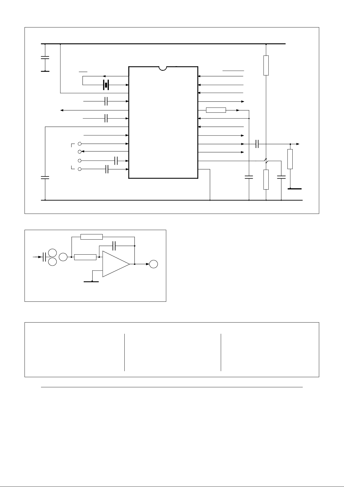
External Components and Interfacing
CTCSS/DATA INPUT
PRE-PROCESS AUDIO OUTPUT
Rx
AUDIO INPUT
POST PROCESS
AUDIO INPUT
MIC. OUTPUT
MIC. INPUT 1
MIC. INPUT 2
XTAL/CLOCK
AUDIO OUTPUT (Rx)
VCO REF. DRIVE (Tx)
COMPRESSION
CAPACITOR
VCO DRIVE (Tx)
R.S.S.I.
NOISE INPUT
NOISE OUTPUT
SQUELCH DRIVE
SERIAL DATA INPUT
SERIAL CLOCK INPUT
R
2
R
1
C
2
C
9
C
4
C
1
C
3
C
6
C
7
C
8
X
1
R
4
Tx AUDIO INPUT
CHIP SELECT
R
3
C
5
SEE
FIG.3
BELOW
13
14
15
16
17
18
19
20
21
22
23
24
1
2
3
4
5
6
7
8
9
10
11
12
FX506P
V
DD
V
DD
V
BIAS
V
SS
V
SS
V
BIAS
V
SS
XTAL
Fig.2 Recommended External Components
Notes
For dual Tx inputs using both Mic.1 and Mic.2 inputs without
pre-emphasis, capacitors C
3
and C4 will be required at the
inputs as shown in Figure 2.
If pre-emphasis is required, the external circuit shown in
Figure 3 is recommended.
The Op-Amp selected for this application should be of a “low
noise wide-bandwidth” type i.e. with at least 60dB of gain at
6kHz.
In addition to the components shown in Figure 2, it is
recommended that the power and V
BIAS
lines to the external
Op-Amp are decoupled to V
SS
physically close to the
amplifier
, by a 1.0µF capacitor.
Layout Recommendations
Audio microcircuit performance will be affected by external
noise.
All external components should be kept as close to
the device as possible.
Tracks to the device should be kept short, particularly
the Audio and V
BIAS
inputs.
A “ground-plane” connected to V
SS
will help to
eliminate external pick-up.
Ensure that all inputs (analogue and d.c.) are free from
noise.
Xtal/clock and digital tracks should be kept well away
from analogue circuitry. Analogue inputs and outputs
should be screened wherever possible with high-level
outputs isolated from very low-level inputs.
Circuit References
Component Value Tolerance
R1= 100kΩ = ± 10%
R
2
390kΩ± 10%
R
3
100kΩ± 1%
R
4
10kΩ± 10%
R
5
18.0kΩ± 1%
R
6
2.7MΩ± 1%
Tx
AUDIO INPUT
+
–
R
5
R
6
EXTERNAL
OP-AMP
BIAS
MIC. I/P
2
MIC. O/P
12
11
MIC. I/P
1
10
9
C
10
/C
4
C
3
C1= 1.0µF ± 20%
C
2
6.8µF ± 20%
C
3
1.0nF ± 1%
C
4
1.0nF ± 1%
C
5
15nF ± 1%
C
6
0.1µF ± 20%
C7= 0.1µF ± 20%
C
8
0.1µF ± 20%
C
9
1.0µF ± 20%
C
10
12.0pF ± 1%
X
1
4.0MHz
Fig.3 Typical 2nd Order Pre-emphasis Input Circuit
Page 5
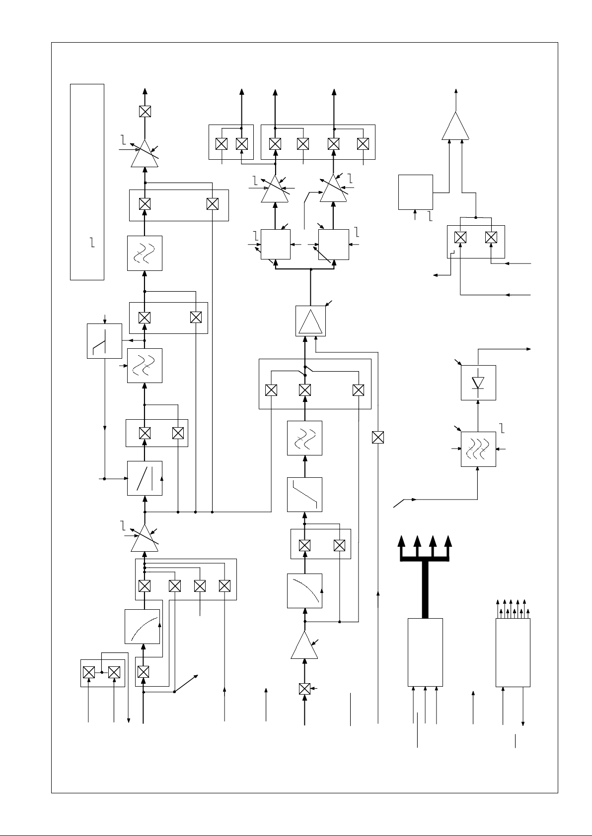
PMR Audio Processor Explanatory Block Diagram
Fig.4 PMR Audio Processor – Facilities
Rx AUDIO INPUT
POST
PROCESS GAIN
PRE-EMPHASIS LIMITER
POST-DEVIATION
LIMITER FILTER
VCO REF
DRIVE (Tx)
VCO
DRIVE (Tx)
AUDIO
OUTPUT (Rx)
OUTPUT DRIVE
POST PROCESS
AUDIO INPUT
INPUT SELECT
# 3, 4, 5, 6
INPUT GAIN AMP
(0 to 15dB)
# 10, 11, 12, 13
COMPRESSOR (VOGAD)
0dB Gain
INPUT HPF PRE-PROCESS GAIN
(-2.75dB to +1.0dB)
COMPRESSION
CAPACITOR
PRE-PROCESS
AUDIO OUTPUT
Test
300Hz
INPUT LPF
16
V
SS
Rx (Noise)
NOISE
OUTPUT
SQUELCH DETECT
SQUELCH
DRIVE
SQUELCH LEVEL
COMPARATOR
-
+
Threshold
(1.5V to 3.5V)
NOISE
INPUT
# 45, 46
R.S.S.I.
# 41, 42, 43, 44
16
Function Control
Bits (#)
SERIAL DATA
INPUT
SERIAL CLOCK
INPUT
#
#
#
#
# 37, 38, 39
XTAL/CLOCK
XTAL
MIC. 1
MIC. 2
MIC. OUTPUT
SQUELCH SELECT
16
# 20, 21, 22
# 23, 24, 25, 26
16
# 40
(Nar./Wide)
PRE-PROCESS PATH
POST-PROCESS PATH
SQUELCH SYSTEM
TEST SIGNAL PATH
V
DD
# 32, 33, 34, 35
# 28, 29, 30, 31
4.0MHz CLOCK
OSCILLATOR
AND
LOGIC
# 15
16
16
8
# 16
(Nar./Wide)
8
(-3.0dB to +4.0dB)
KEY
# = Controlling Logic Bit Number/s
= Adjustable Element, n = Number of steps
= General Powersave
n
Tx AUDIO INPUT
V
BIAS
V
BIAS
DE-EMPHASIS
20dB/dec.
3000Hz
DETECT
Threshold
20dB/dec.
MIXER
AMP
2550Hz
3000Hz
CTCSS/DATA
INPUT
dB
V
BIAS
V
BIAS
V
BIAS
# /
U
DAC
Rx (Noise)
# 1, 2
MIC. SELECT
# 0
(# 7, # 8, # 9 [# 14])
# 14
# 18, 19
OUTPUT DRIVE
SELECT
Test
# 27
# 36
# 36
# 27
SERIAL INPUT
PORT
# 17
GENERAL POWERSAVE
(GPS)
(GPS)
0/14dB
(GPS)
(GPS)
(GPS)
(GPS)
(GPS)
(GPS)
(GPS)
(GPS)
(GPS)
(GPS)
2dB
GPS
∑
CHIP SELECT
dB
(I & II)
5
Page 6
6
Function
Mic. Select
– Microphone Input 1
– Microphone Input 2
Input Select
– Rx Input
De-emphasis Bypass; HPF to 0dB
– Rx Input
De-emphasis Select; HPF to 0dB
– Tx Input
Powersave De-emphasis;
HPF to 14dB
– Path Input to V
BIAS
;
Powersave De-emphasis
Input Gain Amplifier
– Gain Set 0.0dB
1.0dB
2.0dB
3.0dB
4.0dB
5.0dB
6.0dB
7.0dB
8.0dB
9.0dB
10.0dB
11.0dB
12.0dB
13.0dB
14.0dB
15.0dB
Circuit Descriptions and Serial Control Information
...... 1
Control bits
(LSB) loaded last
0
0
1
12
00
01
10
11
3456
0000
1000
0100
1100
0010
1010
0110
1110
0001
1001
0101
1101
0011
1011
0111
1111
78914
111
1
011
1
X01
1
XX0
1
XXX
0
10 11 12 13
0000
1000
0100
1100
0010
1010
0110
1110
0001
1001
0101
1101
0011
1011
0111
1111
14
0
1
Notes
A multiplexed “microphone” input allowing the use
of differing type and level voice inputs.
Transmit or receive audio sources are selected,
inserting the appropriate path gain for the chosen
input.
The input path can be set to bias whilst allowing
receiver noise monitoring.
A gain element intended to adjust the drive level to
the compressor, catering for differing signal
sources and microphone sensitivities.
Reference ...... Figure 4
Compressor HPF LPF Pre-Process Output
Enabled Enabled Enabled Enabled
Powersaved Enabled Enabled Enabled
Powersaved Powersaved Enabled Enabled
Powersaved Powersaved Powersaved Enabled
Powersaved Powersaved Powersaved Powersaved
The Pre-Process Path LPF should be selected whilst CEPT ‘Response to the Tx to Mod.
frequencies exceeding 3kHz’ tests are carried out.
Pre-Process Gain
– Gain Set -2.75dB
-2.50dB
-2.25dB
-2.00dB
-1.75dB
-1.50dB
-1.25dB
-1.00dB
-0.75dB
-0.50dB
-0.25dB
0dB
0.25dB
0.50dB
0.75dB
1.00dB
Pre-Process Output
– Disable Pre-Process Output
Output at V
BIAS
– Enable Pre-Process Audio Output
An in-line output drive stage providing adjustable
gain or attenuation to compensate for level
tolerances in the external audio processes and
peripherals.
The output of this amplifier stage is available for
further voice (audio) processing such as
“Frequency Inversion Voice Scrambling.”
Bit 14 is the Enable/Powersave function for the
Pre-Process output stages.
See
Bits 7 8 9 14 .....
Page 7
7
Circuit Descriptions and Serial Control Information
...... 2
Control bits
15
16
0
1
17
0
1
15 18 19
X 00
010
110
X11
X01
20 21 22
000
100
010
110
001
101
011
111
23 24 25 26
0000
1000
0100
1100
0010
1010
0110
1110
0001
1001
0101
1101
0011
1011
0111
1111
27
Notes
A fixed 2.0dB gain stage.
A selectable pre-emphasis stage set around
1.0kHz, with a characteristic of 6dB per octave.
It is available for use when transmitting data signals
such as FFSK. See Table below for Powersave
information.
A pre-set amplitude limiting stage for deviation
control.
This lowpass filter which is selected with the
Deviation Limiter, is adjustable to Narrow (2550Hz)
and Wide (3000Hz) bandwidths, allowing for
different channel-spacing requirements.
Reference ...... Figure 4
Element
Post-Process Gain
Pre-emphasis
Deviation Limiter
and
Post-Deviation Limiter Filter
– Narrow filter bandwidth,
cut-off = 2550Hz.
– Wide filter bandwidth,
cut-off = 3000Hz.
CTCSS/Data Input
– Disable Input path to Mixer system
– Enable Input path to Mixer system
Pre-Emphasis Limiter and Post-Dev LPF Drive Selected
Powersaved Powersaved Test Path
Powersaved Enabled Post-ProcessPath
Enabled Enabled Post-Process Path
Powersaved Powersaved Post-Process Bypass
Powersaved Powersaved Bias
VCO Reference Drive Attenuator
– Gain Set -28dB
-24dB
-20dB
-16dB
-12dB
-8.0dB
-4.0dB
0.0dB
VCO Reference Drive Amplifier
– Gain Set -2.75dB
-2.50dB
-2.25dB
-2.00dB
-1.75dB
-1.50dB
-1.25dB
-1.00dB
-0.75dB
-0.50dB
-0.25dB
0dB
0.25dB
0.50dB
0.75dB
1.00dB
Output Drive Control
The in-line control attenuator for the VCO reference
channel drive output.
The in-line control amplifier/attenuator for the VCO
reference channel drive output.
Used in conjunction with Bit 36 to control output
functions.
Page 8
8
Circuit Descriptions and Serial Control Information ...... 3
Control bits
28 29 30
000
100
010
110
001
101
011
111
31
0
1
32 33 34 35
0000
1000
0100
1100
0010
1010
0110
1110
0001
1001
0101
1101
0011
1011
0111
1111
27 36
00
01
10
11
37 38 39
000
100
010
110
001
101
011
111
40
0
1
Element
VCO Drive Attenuator I
– Gain Set -22.4dB
-19.2dB
-16.0dB
-12.8dB
-9.6dB
-6.4dB
-3.2dB
0dB
VCO Drive Attenuator II
– Gain Set -25.6dB
0dB
VCO Drive Amplifier
– Gain Set -2.75dB
-2.50dB
-2.25dB
-2.00dB
-1.75dB
-1.50dB
-1.25dB
-1.00dB
-0.75dB
-0.50dB
-0.25dB
0dB
0.25dB
0.50dB
0.75dB
1.00dB
Reference ...... Figure 4
VCO Drive (Tx) VCO Ref (Tx) Audio Output
Output Output (Rx)
Bias Bias Bias
Bias Bias Enabled
Enabled Enabled Bias
Enabled Enabled Enabled
The Drive and Ref. paths are powersaved by Bits 45 and 46 in the “Total Powersave” or
“Listening Powersave” conditions. When making internal changes it is recommended that these
outputs are disconnected
(placed in a bias condition)
from the relevant output (load) circuitry.
Notes
An in-line control attenuator for the VCO Tx channel
drive output.
This channel is also selected as Audio Output (Rx)
under the control of bit 36. This attenuator can be
used in a volume control application.
An in-line control attenuator for the VCO Tx channel
drive output. As an example, when bits 28 to 31 are
set to “0,” the gain set is -48.0dB (-22.4 + -25.6).
The in-line control amplifier/attenuator for the VCO
Tx channel drive output.
This channel is also selected as Audio Output (Rx)
under the control of bit 36. This amplifier can be
used in a volume control application.
Squelch Filter (Gain)
– Gain Set -3.0dB
-2.0dB
-1.0dB
0dB
1.0dB
2.0dB
3.0dB
4.0dB
Squelch Filter (Narrow/Wide)
– Narrow (ƒc ≈ 18kHz ± 6.5kHz).
– Wide (ƒc ≈ 25kHz ± 8.5kHz).
The squelch function is set by bits 45 & 46
(Squelch Source Selection).
The centre frequency gain of this element is 35dB,
data selected gain variations (-3.0dB to 4.0dB) are
around this value.
For use in wide or narrow channel systems.
The squelch function is set by bits 45 & 46
(Squelch Source Selection).
Page 9

9
Circuit Descriptions and Serial Control Information ...... 4
Control bits
41 42 43 44
0000
1000
0100
1100
0010
1010
0110
1110
0001
1001
0101
1101
0011
1011
0111
1111
45 46
00
10
01
11
Rx Noise Path
Test Signal Path
Element
Squelch Threshold Voltage
3.500V d.c. 70.0% V
DD
3.366 67.3%
3.233 64.6%
3.100 62.0%
2.966 59.3%
2.833 56.6%
2.700 54.0%
2.566 51.3%
2.433 48.6%
2.300 46.0%
2.166 43.3%
2.033 40.6%
1.900 38.0%
1.766 35.3%
1.633 32.6%
1.500 30.0%
Squelch Source Selector
A “Total Powersave” condition
Noise Input selected to Comparator
R.S.S.I. input selected to Comparator
Powersave but LISTENING condition
R.S.S.I. input selected to Comparator
Notes
The fine squelch adjustment level from the Digitalto-Analogue converter.
These threshold levels are used as a comparison
with the selected input noise voltage (bits 45 and
46).
Variation in V
DD
will produce variation in threshold
levels.
As well as selecting the input to the Noise
Comparator, these two bits produce additional
General Powersave (GPS) functions which control
those elements not having individual serial control.
Powersaved: Input Gain Amp – Post Process
(2dB) Gain Amp – Mixer Amp – Noise BPF –
Noise Rectifier – Squelch Comparator
Powersaved: Input Gain Amp – Post Process
(2dB) Gain Amp – Mixer Amp – Noise BPF –
Noise Rectifier
Reference ...... Figure 4
Any high-frequency noise (18kHz/25kHz) present at the Rx Audio Input will also be available at
the Noise Output pin via the squelch filter and noise rectifier (when enabled) for use as a
squelch detection level. This means that the FX506 can be set to “LISTEN” with the majority of
circuit elements powersaved until an R.S.S.I. level is detected and produces a "Squelch Drive
output."
This path, when selected, can be used as a direct path, via the Output Drive Selector
(bits 18 and 19), to dynamically set and balance the VCO drive and reference output levels.
Page 10
10
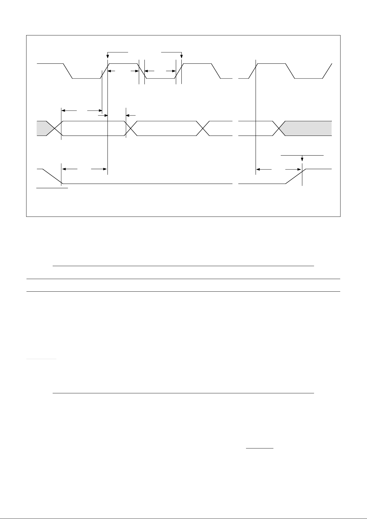
Serial Control Bits – Loading and Timing Information
SERIAL CLOCK IN
t
PWL
t
CSH
SERIAL DATA IN
t
DS
t
DH
bit 46 bit 44
t
PWH
Data Clocked
t
CSS
bit 45
- loaded first
[1]
[1]
[3]
[2]
bit 0
- loaded last
47-bit Data Word Latched
CHIP SELECT
Fig.5 Data Load Timing Diagram
Data Loading
Serial Data bits, whose functions are described on the previous pages, are loaded to the FX506 using
the timing format illustrated on this page. All 47 bits must be loaded. Data is loaded bit 46 first, bit 0 last.
Function Min. Typ. Max. Unit
Serial Clock [1]
‘High’ Pulse Width t
PWH
600 – – ns
‘Low’ Pulse Width t
PWL
600 – – ns
Serial Data [2]
Data Set-Up Time t
DS
360 – – ns
Data Hold Time t
DH
120 – – ns
Chip Select [3]
Select Set-Up Time t
CSS
600 – – ns
Select Hold Time t
CSH
600 – – ns
[1] The Serial Clock pulses do not have to be symmetrical, as shown above, but pulse lengths must
conform to the “minimum” time specification.
[2] Individual data bits (logic “1” or “0”) are loaded to the device on the rising edge of the input Serial
Data
Clock pulse. The data hold period (tDH) is to ensure that the data level is steady when it is
sampled.
[3] The full 47-bit data word is latched into the device on the rising edge of the Chip Select waveform,
at this time the loaded data is acted upon and the circuit configuration/settings will change.
Page 11
11
System Response Characteristics
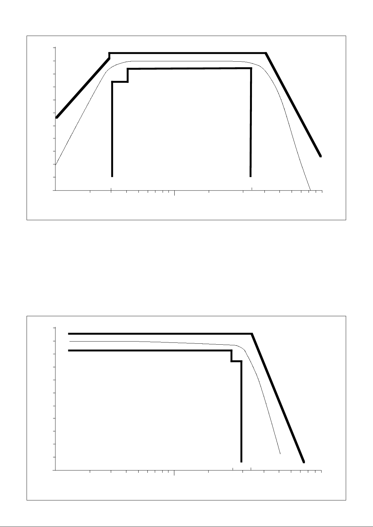
Fig.7 Typical Post-Process Path Frequency Response
-16
-14
-12
-10
-18
-8
-6
-4
-2
0
2
-20
200 500 1000 2000 5000 10000
Frequency (Hz)
Gain (dB)
300 3400
Fig.6 Typical Pre-Process Path Frequency Response
-16
-14
-12
-10
-18
-8
-6
-4
-2
0
2
-20
200 500 1000 2000 5000 10000
Frequency (Hz)
Gain (dB)
2700 3400
System Frequency Characteristics
Figure 6 shows a typical, response curve of the Pre-Process Path, in receive mode, set against the
device specification. The general characteristic shape is produced by the Input Highpass and Lowpass
Filters, without the internal pre-emphasis element.
Figure 7 shows a typical response curve of the Post-Process Path set against the device specification.
The general characteristic shape is produced by the Post-Deviation Limiter Filter, without the deemphasis element.
Page 12
12
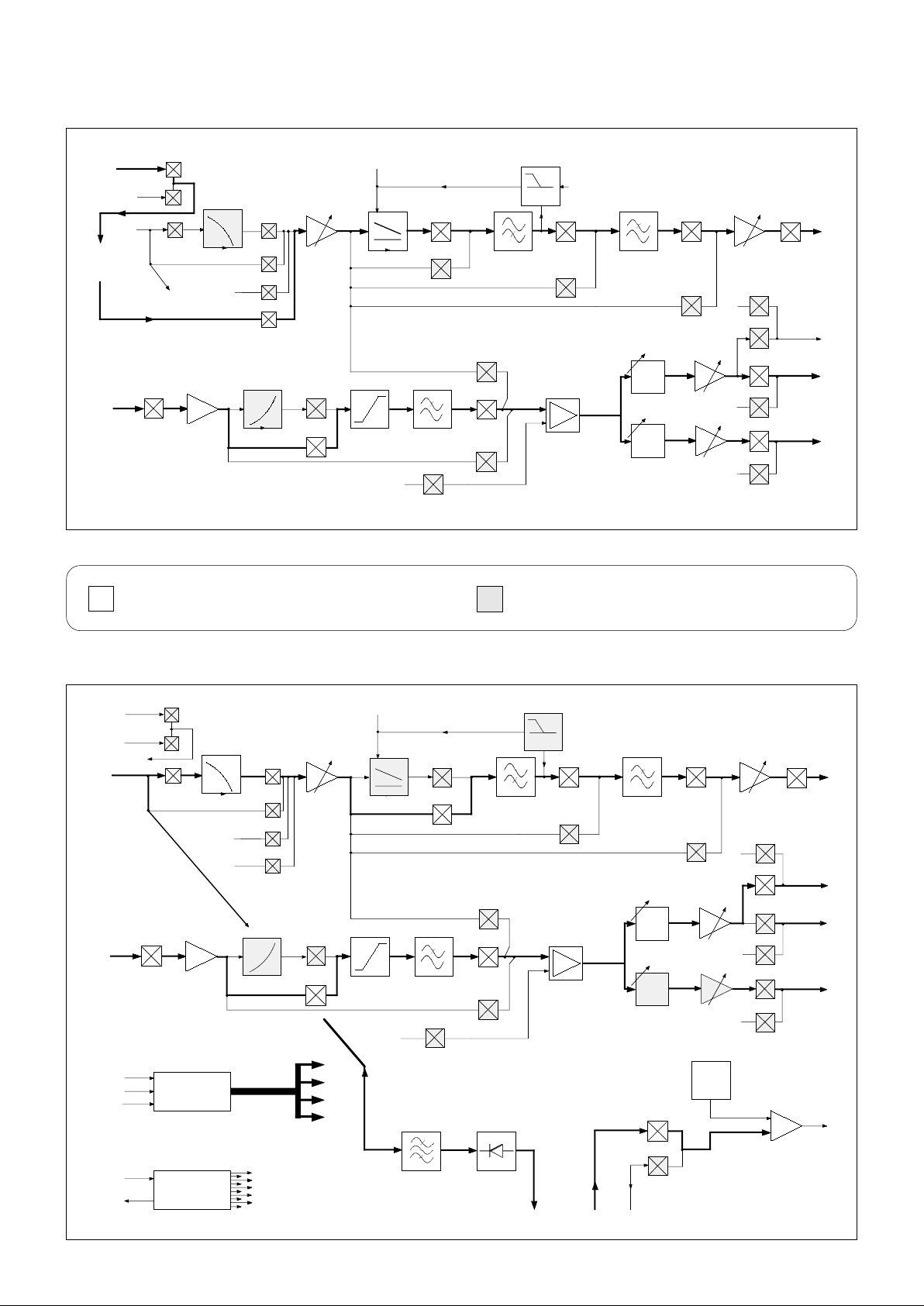
Application Information ......
Suggested Evaluation Tests and Settings
Fig.9 Receive and Squelch Paths – Suggested Test Settings
VCO REF
DRIVE (Tx)
VCO
DRIVE (Tx)
POST PROCESS
AUDIO INPUT
COMPRESSION
CAPACITOR
PRE-PROCESS
AUDIO OUTPUT
300Hz
MIC. 1
MIC. OUTPUT
PRE-PROCESS PATH
POST-PROCESS PATH
Tx AUDIO INPUT
3000Hz
DETECT
2dB
2550Hz
3000Hz
dB
dB
Test
To
External
Audio Processes
From
External Audio
Processes
20dB/dec.
2.2V p-p (100%)
Output Level
0dB
0dB
0dB
0dB
755mVrms
600mVrms
600mVrms
0dB
710mVrms
710mVrms
14dB
0dB
158mVrms
10mVrms
24dB
External
Gain
158mVrms
2.2V p-p (100%)
Output Level
20dB/dec.
∑
CTCSS/DATA
Fig.8 Transmit Path – Suggested Test Settings
Rx AUDIO INPUT
AUDIO
OUTPUT (Rx)
INPUT H.P.F.
PRE-PROCESS
AUDIO OUTPUT
300Hz
Rx (Noise)
NOISE
OUTPUT
SQUELCH
DRIVE
-
+
NOISE
INPUT
PRE-PROCESS PATH
POST-PROCESS PATH
SQUELCH SYSTEM
20dB/dec.
3000Hz
DETECT
20dB/dec. 2550Hz
3000Hz
dB
# /
U
DAC
Rx (Noise)
dB
2.2V p-p
(100%)
0dB 0dB
710mVrms
564mVrms
564mVrms
-2.0dB
0dB
11dB
710mVrms
200mVrms
2dB
∑
Active elements used in the signal path. Powersaved or by-passed elements that are not
employed in the signal path.
Page 13
13
Operational Information
The functions of the FX506 are selected and controlled using the 47-bit Serial Data Input. This
application section assists in the familiarization of control by providing example operational paths
and system confidence tests.
The signal levels employed in these examples are to demonstrate the functions of the device.
Maximum and minimum operational signal levels are detailed in the “Specification” pages. A final
output signal level of 2.2V p-p is considered, operationally, to be 100% (FM deviation).
Set-up and enter the example data word in accordance with Figures 2 and 4.
Test the FX506 using levels and points detailed in Tables 1, 2 and 3.
Experimentation will indicate the signal element configuration and required control settings for
various input and output levels.
Application Information
Suggested Evaluation Tests and Settings
Transmit Path –
The Serial Data word below will produce the transmit element configuration shown in Figure 8.
bit 0 – 01000001 11110110 X0101111 10111111 11010XXX XXXXX10 – bit 46
0 = logic 0 1 = logic 1 X = not important to the example
Step Input – Level Output – Level Note Output Level
(mV rms @ 1kHz) (mV rms @ 1kHz)
Ref. to Max.
1 Mic. 1 10 Pre-Process Audio 750 Ext +24.0dB
2 Ext. Audio Process In 750 VCO Drive/Ref. 1.54≤ V
OUT
≤2.2Vp-p 70 – 100%
3 Mic. 1 4.8 Pre-Process Audio 410 Ext +24.0dB 60%
4 Ext. Audio Process In 410 VCO Drive and Ref. 466 60%
Table 1 Transmit Path Operational Check
To establish a 100% level for this device inject a large amplitude audio signal into the Post Process
Audio Input, with the Limiter enabled.
Squelch Path –
The Serial Data word below will produce the squelch element configuration shown in Figure 9.
bit 0 – X00XXXXX XXXXXX0X X010XXXX XXX0XXXX XXXX1110 1110110 – bit 46
0 = logic 0 1 = logic 1 X = not important to the example
Step Input – Level Output – Level Note
(mV rms @ 25kHz)
1 Rx Audio In 0 Squelch Drive logic “1” No noise – “Noise Out” = V
BIAS
2 Rx Audio In 50.0 Squelch Drive logic “0” Noise In – “Noise Out” decreases
Table 3 Squelch Path Operational Check
Receive Path –
The Serial Data word below will produce the receive element configuration shown in Figure 9.
bit 0 – X0111010 11110010 X010XXXX XXX01111 11011XXX XXXXX10 – bit 46
0 = logic 0 1 = logic 1 X = not important to the example
Step Input – Level Output – Level Note Output Level
(mV rms @ 1kHz) (mV rms @ 1kHz)
Ref. to Max.
1 Rx Audio In 200 Pre-Process Audio 564
2 Ext. Audio Process In 564 Audio Out (Rx) 1.54≤ V
OUT
≤2.2Vp-p 70 -100%
3 Rx Audio In 145 Audio Out (Rx) 466 60%
4 Rx Audio In 145 Audio Out (Rx) 466± 60%±
vary bits 28 – 35 for Volume
Table 2 Receive Path Operational Check
To establish a 100% level for this device inject a large amplitude audio signal into the Post Process
Audio Input, with the Limiter enabled.
Page 14

14
Specification
Absolute Maximum Ratings
Exceeding the maximum rating can result in device damage. Operation of the device outside the operating limits is not implied.
Supply voltage -0.3 to 7.0V
Input voltage at any pin (ref V
SS
= 0V) -0.3 to (V
DD
+ 0.3V)
Sink/source current (supply pins) +/- 30mA
(other pins) +/- 20mA
Total device dissipation @ T
AMB
25°C 800mW Max.
Derating 10mW/°C
Operating temperature range: FX506P -30°C to +70°C (plastic)
FX506LG/LS -30°C to +70°C (plastic)
Storage temperature range: FX506P -40°C to +85°C (plastic)
FX506LG/LS -40°C to +85°C (plastic)
Operating Limits
All device characteristics are measured under the following conditions unless otherwise specified:
V
DD
= 5.0V. T
AMB
= 25°C. Xtal/Clock f0 = 4.0MHz. Audio level 0dB ref: = 466mV rms @ 1.0kHz
(60% deviation, FM)
.
Characteristics See Note Min. Typ. Max. Unit
Static Values
Supply Voltage 4.5 5.0 5.5 V
Supply Current (All Elements Enabled) – 8.0 – mA
(Listening Powersave) – – 1.0 mA
(Maximum Powersave) – – 1.0 mA
Dynamic Values
Input Logic “1” 1 3.5 – – V
Input Logic “0” 1 – – 1.5 V
Input Impedances
Digital 0.1 1.0 – MΩ
Mic.1 or 2 – 0.5 – kΩ
Rx Audio 30.0 – – kΩ
Tx Audio 30.0 56.0 – kΩ
CTCSS/Data 50.0 100 – kΩ
External Audio Process 1.0 – – MΩ
Noise, R.S.S.I. 1.0 – – MΩ
Output Impedances
Pre-Process Audio – – 3.0 kΩ
Audio Out (Rx) – – 3.0 kΩ
VCO Drive and Ref. Out – – 3.0 kΩ
Squelch Drive (Logic “1”) – 5.0 – kΩ
(Logic “0”) – 500 – Ω
Noise Output (Diode conducting) – 1.0 – kΩ
(Diode not conducting) – 500 – kΩ
Signal Path Switch Isolation (Disabled)
Switches 40.0 – – dB
Test Path – 60.0 – dB
Signal Input Levels 10
Mic.1 or 2 1.0 – 100 mV rms
Rx Audio – 145 200 mV rms
Tx Audio – – 1414 mV rms
CTCSS/Data – – 4.0 V p-p
Post Process – – 1123 mV rms
Noise, R.S.S.I. 2 – – 4.0 V p-p
Signal Output Levels 10
Pre-Process Audio (Compressor enabled) – 600 – mV rms
VCO – (Drive, Ref.) (Limiter in circuit) – 2.2 – V p-p
Audio (Rx (Limiter in circuit) – 2.2 – V p-p
Variable Element Step
Input Gain Amp 0.7 1.3 dB
Pre-Process Gain 0.2 0.3 dB
VCO Ref. Attenuator 3.5 4.5 dB
VCO Drive Attenuator I 2.7 3.7 dB
VCO Drive Attenuator II 25.0 26.2 dB
VCO Amplifiers (Drive and Ref.) 0.2 0.3 dB
Page 15

15
Output Distortion
Output Signal-to-Noise Ratio 3, 12 48.0 52.0 – dBp
Total Harmonic Distortion Level 4, 11 – -40.0 -30.0 dB
Compressor
Dynamic Range – 30.0 – dB
Attack Time – 7.0 – ms
Decay Time – 1000 – ms
Deviation Limiter
Input Thresholds 4 – 2.0 – V p–p
Frequency Responses
Pre-Process Path 6
Passband Frequencies
-3dB (Lower) – 240 – Hz
-3dB (Upper) – 4.7 – kHz
Passband Ripple (300Hz - 400Hz) 5 -3.0 – 1.0 dB
(400Hz - 3400Hz) 5 -1.5 – 1.0 dB
Stopband Attenuation (ƒ = 5kHz) 3.0 4.2 – dB
High Frequency Roll-off (ƒ = >5kHz, <20kHz) 12.0 – – dB/oct.
Stopband Attenuation (ƒ = 250Hz) – 2.3 – dB
Low Frequency Roll-off (ƒ = <250Hz) 6.0 – – dB/oct.
Post-Process Path 7
Wideband : Lowpass Frequency (-3dB) – 3.4 – kHz
Passband Ripple (< 2700Hz) 8 -1.5 – 1.0 dB
(2700Hz - 3000Hz) 8 -3.0 – 1.0 dB
Stopband Attenuation (ƒ = 5kHz) 12.2 17.0 – dB
High Frequency Roll-off (ƒ = >3kHz, <20kHz) 18.0 – – dB/oct.
Narrowband: Lowpass Frequency (-3dB) – 2.9 – kHz
Passband Ripple (< 2300Hz) -1.5 – 1.0 dB
(2300Hz - 2550Hz) -3.0 – 1.0 dB
Stopband Attenuation (ƒ = 4.25kHz) 12.2 17.0 – dB
High Frequency Roll-off (ƒ = >2.3kHz, <5.1kHz) 18.0 – – dB/oct.
Pre-emphasis: Passband Frequencies 300 3000 Hz
Gain at 1kHz – 0 – dB
Slope Characteristic – 6.0 – dB/oct.
De-emphasis: Passband Frequencies 300 3000 Hz
Gain at 1kHz – 0 – dB
Slope Characteristic – 6.0 – dB/oct.
Squelch Bandpass Filter
Centre Frequency Gain (Wide and Narrow) – 35.0 – dB
Selectable Gain (8 x 1.0dB steps) 9 -3.0 – 4.0 dB
Narrow Band:
Centre Frequency (ƒc) – 18.75 – kHz
Bandwidth (ƒc ±) – 6.5 – kHz
Wideband:
Centre Frequency (ƒc) – 25.5 – kHz
Bandwidth (ƒc ±) – 8.5 – kHz
Notes
1. A percentage of the applied V
DD
(70% or 30%).
2. These inputs are compared internally with the Digital-to-Analogue converter.
3. With a minimum signal input level of 50mVrms at the Tx I/P or 65mVrms at the Rx I/P and an output level of
466mVrms.
4. Levels at the input of the Limiter element, centred about V
BIAS
(Note 2).
5. This parameter remains within specification when pre-emphasis is employed.
6. With both Input HPF and LPF in circuit, but without pre-emphasis.
7. With Limiter LPF, but without de-emphasis characteristics.
8. This parameter remains within specification when de-emphasis is employed.
9. The gain variation around the centre frequency (ƒc).
10. See Application Information pages (Suggested Evaluation Tests) for information on gain element settings.
11. Mode: Tx with Compressor “OFF;” or in Rx, signal below limiter thresholds; Output level 466mVrms.
Measured in a 30kHz bandwidth.
12. In the Tx mode with the Input Gain Amp set to ≤ 4.0dB.
Specification ......
Characteristics See Note Min. Typ. Max. Unit
Page 16

Handling Precautions
The FX506 is a CMOS LSI circuit which includes input
protection. However precautions should be taken to
prevent static discharges which may cause damage.
CML does not assume any responsibility for the use of any circuitry described. No circuit patent licences are implied
and CML reserves the right at any time without notice to change the said circuitry.
Ordering Information
FX506LG 24-pin encapsulated bent and
cropped (L1)
FX506LS 24-lead plastic leaded chip
carrier (L2)
FX506P 24-pin plastic DIL (P4)
Package Outlines
The FX506 is available in the package styles outlined
below. Mechanical package diagrams and specifications
are detailed in Section 10 of this document.
Pin 1 identification marking is shown on the relevant
diagram and pins on all package styles number
anti-clockwise when viewed from the top.
NOT TO SCALE
Max. Body Length 10.25mm
Max. Body Width 10.25mm
FX506LG 24-pin quad plastic encapsulated
bent and cropped (L1)
NOT TO SCALE
Max. Body Length 10.40mm
Max. Body Width 10.40mm
FX506LS 24-lead plastic leaded chip carrier
(L2)
FX506P 24-pin plastic DIL (P4)
NOT TO SCALE
Max. Body Length 31.85mm
Max. Body Width 13.82mm
 Loading...