

Page 1

CML Semiconductor Products
Calling Line Identifier
1.0 Features Provisional Information
•• CLI and CIDCW Detector with:
•• On-Hook and Off-Hook Operation •• Low Voltage Operation
•• 'Zero-Power' Ring or Line Polarity
Reversal Detector
•• V23/Bell202 FSK Demodulator
with Data Retiming facility
•• Dual-Tone Alert Detector •• 16-pin SOIC and DIL packages
•• For Bellcore, ETSI, British Telecom
and Mercury Systems
••µµC Interrupt/Wake-up output to
minimise system operating power
FX602
D/602/5 April 1996
1.1 Brief Description
The FX602 is a low power CMOS integrated circuit for the reception of the physical layer signals used in BT's
Calling Line Identification Service (CLIP), Bellcore's Calling Identity Delivery system (CID), the Cable
Communications Association's Caller Display Services (CDS), and similar evolving services. It also meets the
requirements of emerging Caller Identity with Call Waiting services.
The device includes a 'zero-power' ring or line polarity reversal detector, a dual-tone (2130Hz plus 2750Hz)
Tone Alert Signal detector and a 1200-baud FSK V23/Bell202 compatible asynchronous data demodulator with
a data retiming circuit which removes the need for a UART in the associated µC.
It is suitable for use in systems to BT specifications SIN227 and SIN242, Bellcore TR-NWT-000030 and SRTSV-002476, CCA TW/P&E/312, ETSI ETS 300 659 parts 1 and 2, and Mercury Communications MNR 19.
1996 Consumer Microcircuits Limited
Page 2

Calling Line Identifier FX602
CONTENTS
Section Page
1.0 Features..........................................................................................................1
1.1 Brief Description............................................................................................1
1.2 Block Diagram................................................................................................3
1.3 Signal List.......................................................................................................4
1.4 External Components....................................................................................6
1.5 General Description.......................................................................................7
1.5.1 Mode Control Logic .........................................................................7
1.5.2 Input Signal Amplifier.......................................................................7
1.5.3 Bandpass Filter................................................................................8
1.5.4 Level Detector ................................................................................. 8
1.5.5 FSK Demodulator............................................................................9
1.5.6 FSK Data Retiming..........................................................................9
1.5.7 Tone Alert Detector ....................................................................... 10
1.5.8 Ring or Line Polarity Reversal Detector ........................................11
1.5.9 Xtal Osc and Clock Dividers..........................................................13
1.6 Application Notes........................................................................................14
1.6.1 'On-Hook' Operation......................................................................14
1.6.2 'Off-Hook' Operation......................................................................15
1.7 Performance Specification .........................................................................24
1.7.1 Electrical Performance .................................................................. 24
1.7.2 Packaging......................................................................................28
1996 Consumer Microcircuits Limited 2 D/602/5
Page 3
Calling Line Identifier FX602
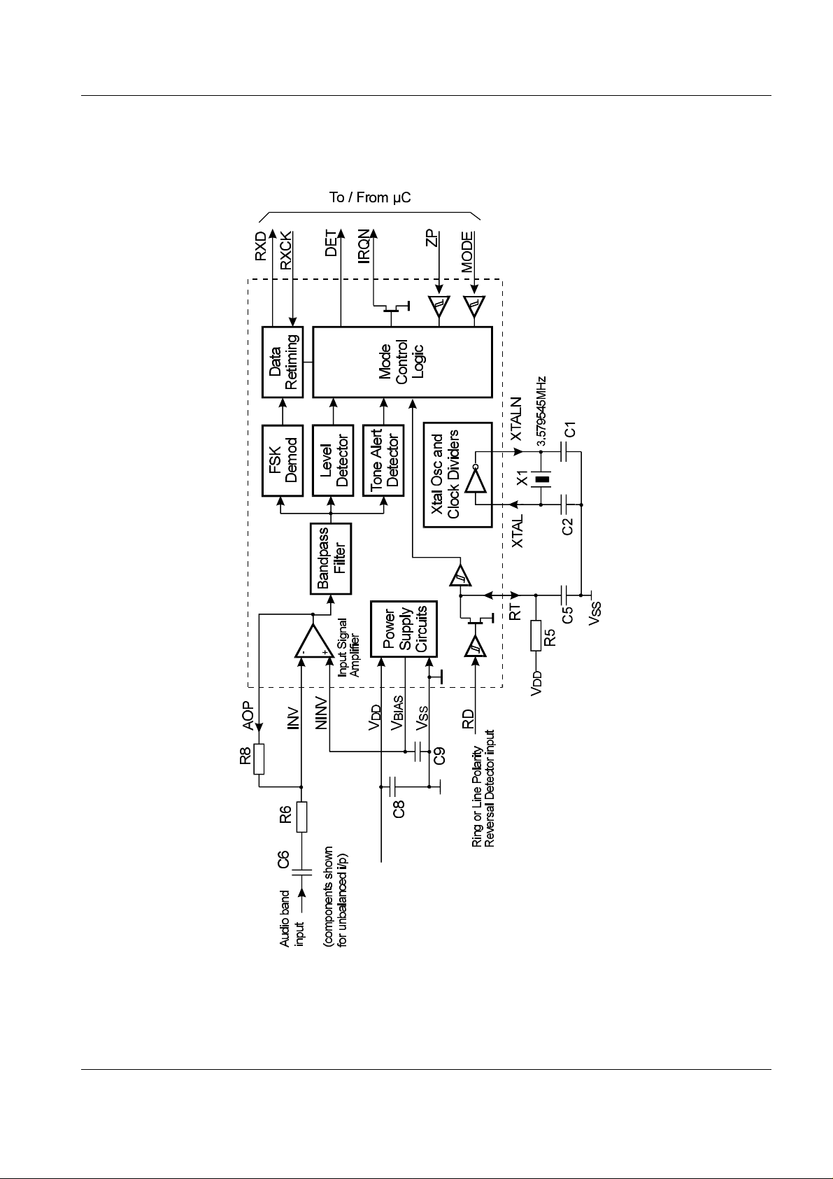
1.2 Block Diagram
Figure 1 Block Diagram
1996 Consumer Microcircuits Limited 3 D/602/5
Page 4

Calling Line Identifier FX602
1.3 Signal List
Packages
D4 / P3
Signal Description
Pin No. Name Type
1 XTALN O/P The output of the on-chip Xtal oscillator inverter.
2 XTAL I/P The input to the on-chip Xtal oscillator inverter.
3 RD I/P (S) Input to the Ring or Line Polarity Reversal
Detector.
4 RT BI Open-drain output and Schmitt trigger input
forming part of the Ring or Line Polarity Reversal
detector. An external resistor to V
capacitor to V
should be connected to RT to
SS
DD
and a
filter and extend the RD input signal.
5 AOP BI The output of the on-chip Input Signal Amplifier
and the input to the Bandpass Filter.
6 INV I/P The inverting input to the on-chip Input Signal
Amplifier.
7 NINV I/P The non-inverting input to the on-chip Input
Signal Amplifier.
8 V
9 V
SS
BIAS
Power Negative supply rail (signal ground).
O/P Internally generated bias voltage, held at VDD/2
when the device is not in 'Zero-Power' mode.
Should be decoupled to V
by a capacitor
SS
mounted close to the device pins.
10 MODE I/P (S) Input used to select the operating mode. See
section 1.5.1.
11 ZP I/P (S) A high level on this input selects 'Zero-Power'
mode, a low level enables the Input Signal
Amplifier, the Bandpass Filter and either the FSK
or the Tone Alert circuits depending on the
MODE input.
1996 Consumer Microcircuits Limited 4 D/602/5
Page 5

Calling Line Identifier FX602
Packages
D4 / P3
Signal Description
Pin No. Name Type
12 IRQN O/P An open-drain active low output that may be
used as an Interrupt Request / Wake-up input to
the associated µC. An external pull-up resistor
should be connected between this output and
.
V
DD
13 DET O/P A logic level output driven by the Ring or Line
Polarity Reversal Detector, the Tone Alert
Detector or the FSK Level detect circuits,
depending on the operating mode. See section
1.5.1.
14 RXCK I/P A logic level input which may be used to clock
received data bits out of the FSK Data Retiming
block.
15 RXD O/P A logic level output carrying either the raw output
of the FSK Demodulator or re-timed 8-bit
characters depending on the state of the RXCK
input. See section 1.5.6
16 V
DD
Notes: I/P = Input
I/P (S) = Schmitt trigger input
O/P = Output
BI = Bidirectional
Power The positive supply rail. Levels and thresholds
within the device are proportional to this voltage.
Should be decoupled to VSS by a capacitor
mounted close to the device pins.
1996 Consumer Microcircuits Limited 5 D/602/5
Page 6
Calling Line Identifier FX602
µ
µ
µ
1.4 External Components
R1
470k
Ω
R2 See section 1.5.8 C1, C2 18pF
R3, R4, R5
R6, R7
R8
470k
470k
470k
680k
Ω
Ω
Ω for V
Ω for V
= 3.3V
DD
DD
= 5.0V
C3, C4
C5
C6, C7
C8,C9
0.1
0.33
680pF
0.1
(See section 1.5.2)
R9
240k
200k
Ω for V
Ω for V
= 3.3V
DD
= 5.0V
DD
(See section 1.5.2)
R10
R11
Ω
160k
Ω ±20%
100k
Resistors
±1%, capacitors ±20% unless otherwise stated.
X1 3.579545MHz
D1 - D4 1N4004
Figure 2 Recommended External Components for Typical Application
F
F
F
1996 Consumer Microcircuits Limited 6 D/602/5
Page 7
Calling Line Identifier FX602
1.5 General Description
1.5.1 Mode Control Logic
The FX602's operating mode and the source of the DET and IRQN outputs are determined by the logic levels
applied to the MODE and ZP input pins;
ZP MODE Mode DET o/p from IRQN o/p from
0 0 Tone Alert Detect Tone Alert Signal
Detection
0 1 FSK Receive FSK Level Detector FSK Data Retiming
1 0 'Zero-Power' Ring or Line Polarity
Reversal Detector.
1 1 'Zero-Power' Ring or Line Polarity
Reversal Detector.
[1]
If enabled.
End of Tone Alert Signal.
Ring or Line Polarity
Reversal Detector.
[1]
.
Ring or Line Polarity
Reversal Detector.
Ring or Line Polarity
Reversal Detector.
-
In the 'Zero-Power' modes, power is removed from all of the internal circuitry except for the Ring or Line
Polarity Reversal Detector and the DET and IRQN outputs.
1.5.2 Input Signal Amplifier
This amplifier is used to convert the balanced FSK and Tone Alert signals received over the telephone line to
an unbalanced signal of the correct amplitude for the FSK receiver and Tone Alert Detector circuits.
Figure 3a : Input Signal Amplifier, balanced input configuration
The design equations for this circuit are;
Differential voltage gain V
R6 = R7 = 470k
Ω
/ V(b-a) = R8/R6
AOP
R10 = 160kΩ
R9 = R8 x R10 / (R8 - R10)
The target differential voltage gain depends on the expected signal levels between the A and B wires and the
FX602's internal threshold levels, which are proportional to the supply voltage.
The FX602 has been designed to meet the applicable specifications with R8 = 470k
rising to 680k
Ω at V
= 5.0V, and R9 should be 240kΩ at V
DD
= 3.3V and 200kΩ at V
DD
Ω at V
= 3.3V nominal,
DD
= 5.0V as shown in
DD
section 1.4 and Fig 3c.
1996 Consumer Microcircuits Limited 7 D/602/5
Page 8
Calling Line Identifier FX602
R8 and R9 : k ohms
The Input Signal Amplifier may also be used with an unbalanced signal source as shown in Figure 3b. The
values of R6 and R8 are as for the balanced input case.
Figure 3b : Input Signal Amplifier, unbalanced input configuration
1000
900
800
700
R8
600
500
400
300
R9
200
100
0
3 3.5 4 4.5 5 5.5
Nominal V
Figure 3c : Input Signal Amplifier, optimum values of R8 and R9 vs V
1.5.3 Bandpass Filter
Is used to attenuate out of band noise and interfering signals which might otherwise reach the FSK
Demodulator, Tone Alert Detector and Level Detector circuits. The characteristics of this filter differ in FSK and
Tone Alert modes. Most of the filtering is provided by Switched Capacitor stages clocked at 57.7kHz.
1.5.4 Level Detector
DD
DD
This block operates by measuring the level of the signal at the output of the Bandpass Filter, and comparing it
against a threshold which depends on whether FSK Receive or Tone Alert Detect mode has been selected.
In Tone Alert Detect mode the output of the Level Detector block provides an input to the Tone Alert Signal
Detector.
1996 Consumer Microcircuits Limited 8 D/602/5
Page 9

Calling Line Identifier FX602
µ
µ
µ
µ
In FSK Receive mode the FX602 DET output will be set high when the level has exceeded the threshold for
sufficient time. Amplitude and time hysteresis are used to reduce chattering of the DET output in marginal
conditions.
Note that in FSK Receive mode this circuit may also respond to non-FSK signals such as speech.
See section 1.7.1 for definitions of Teon and Teoff
Figure 4 : FSK Level Detector operation
1.5.5 FSK Demodulator
This block converts the 1200 baud FSK input signal to a logic level received data signal which is output via the
RXD pin as long as the Data Retiming function is not enabled (see section 1.5.6). This output does not depend
on the state of the FSK Level Detector output.
Note that in the absence of a valid FSK signal, the demodulator may falsely interpret speech or other
extraneous signals as data.
1.5.6 FSK Data Retiming
The Data Retiming block extracts the 8 data bits of each character from the received asynchronous data
stream, and presents them to the
C under the control of strobe pulses applied to the RXCK input. The timing
of these pulses is not critical and they may easily be generated by a simple software loop. This facility removes
the need for a UART in the
C without incurring an excessive software overhead.
The block operates on a character by character basis by first looking for the mark to space transition which
signals the beginning of the start bit, then, using this as a timing reference, sampling the output of the FSK
Demodulator in the middle of each of the following 8 received data bits, storing the results in an internal 8-bit
shift register.
When the eighth data bit has been clocked into the internal shift register, the FX602 examines the RXCK input.
If this is low then the IRQN output will be pulled low and the first of the stored data bits put onto the RXD output
pin. On detecting that the IRQN output has gone low, the
C should pulse the RXCK pin high 8 times. The high
to low transition at the end of the first 7 of these pulses will be used by the FX602 to shift the next data bit from
the shift register onto the RXD output. At the end of the eighth pulse the FSK Demodulator output will be
reconnected to the RXD output pin. The IRQN output will be cleared the first time the RXCK input goes high.
Thus to use the Data Retiming function, the RXCK input should be kept low until the IRQN output goes low; if
the Data Retiming function is not required the RXCK input should be kept high.
The only restrictions on the timing of the RXCK waveform are those shown in Figure 5a and the need to
complete the transfer of all eight bits into the
C within 8.3mSec (the time of a complete character at 1200
baud).
1996 Consumer Microcircuits Limited 9 D/602/5
Page 10

Calling Line Identifier FX602
td = Internal FX602 delay; max. 1µS tclo = RXCK low time; min 1µS tchi = RXCK high time; min 1µS
Figure 5a : FSK Operation With Data Retiming
Note that, if enabled, the Data Retiming block will interpret the FSK Channel Seizure signal (a sequence of
alternating mark and space bits) as valid received characters, with values of 55 (hex). Similarly it may interpret
speech or other signals as random characters.
If the Data Retiming facility is not required, the RXCK input to the FX602 should be kept high. The
asynchronous data from the FSK Demodulator will then be connected directly to the RXD output pin, and the
IRQN output will not be activated by the FSK signal. This case is illustrated in Figure 5b.
Figure 5b : FSK Operation Without Data Retiming (RXCK always high)
1.5.7 Tone Alert Detector
This block is enabled when the FX602 is set to Tone Alert Detector operating mode. It will then monitor the
received signal for the presence of simultaneous 2130 and 2750Hz tones of sufficient level and duration.
The FX602 DET output will be set high while a valid Tone Alert signal is detected. At the end of the Tone Alert
signal the DET output will go low and the IRQN output will be pulled low until the FX602 is switched out of Tone
Alert Detector mode.
1996 Consumer Microcircuits Limited 10 D/602/5
Page 11

Calling Line Identifier FX602
See section 1.7.1 for definitions of Tton and Ttoff
Figure 6 : Tone Alert Detector operation
1.5.8 Ring or Line Polarity Reversal Detector
These circuits are used to detect the Line Polarity Reversal and Ringing signals associated with the Calling
Line Identification protocol.
Figure 7 illustrates their use in a typical application.
Figure 7 : Ring or Line Polarity Reversal operation
1996 Consumer Microcircuits Limited 11 D/602/5
Page 12

Calling Line Identifier FX602
µ
µ
When no signal is present on the telephone line, RD will be at VSS and RT pulled to VDD by R5 so the output of
the Schmitt trigger 'B' will be low.
The ring signal is usually applied at the subscriber's exchange as an ac voltage inserted in series with one of
the telephone wires and will pass through either C3 and R3 or C4 and R4 to appear at the top end of R1 (point
X in Figure 7) in a rectified and attenuated form.
The signal at point X will be further attenuated by the potential divider formed by R1 and R2 before being
applied to the FX602 input RD . If the amplitude of the signal appearing at RD is greater than the input
threshold (Vthi) of Schmitt trigger 'A' then the N transistor connected to RT will be turned on, pulling the voltage
at RT to V
by discharging the external capacitor C5. The output of the Schmitt trigger 'B' will then go high,
SS
activating the DET and/or IRQN outputs depending on the states of the MODE and ZP inputs.
The minimum amplitude ringing signal that is certain to be detected is
( 0.7 + Vthi x [R1 + R2 + R3] / R2 ) x 0.707 Vrms
where Vthi is the high-going threshold voltage of the Schmitt trigger A (see section 1.7).
With R1, R3 and R4 all 470k
of 40Vrms and above for V
Ω as Figure 2, then setting R2 to 68kΩ will guarantee detection of ringing signals
over the range 3.0 to 5.5V.
DD
A line polarity reversal may be detected using the same circuit but there will be only one pulse at RD. The BT
specification SIN242 says that the circuit must detect a +15V to -15V reversal between the two lines slewing in
30msec. For a linearly changing voltage at the input to C3 (or C4), then the voltage appearing at the RD pin will
be
dV/dt x C3 x [ 1 - exp(-t/T) ] x R2
where T = C3 x (R1 + R2 + R3) and dV/dt is the input slew rate.
For dV/dt = 500V/sec (15V in 30msec), R1, R3 and R4 all 470k
setting R2 to 390k
Ω will guarantee detection at V
= 5.5V.
DD
Ω and C3, C4 both 0.1
F as Figure 2, then
If the time constant of R5 and C5 is large enough then the voltage on RT will remain below the threshold of the
'B' Schmitt trigger keeping the DET and/or IRQN outputs active for the duration of a ring cycle
The time for the voltage on RT to charge from V
VRT = V
As the Schmitt trigger high-going input threshold voltage (Vthi) has a minimum value of 0.56 x V
towards VDD can be derived from the formula
SS
x [1 - exp(-t/(R5 x C5)) ]
DD
, then the
DD
Schmitt trigger B output will remain high for a time of at least 0.821 x R5 x C5 following a pulse at RD.
Using the values given in Figure 2 (470k
Ω and 0.33
F) gives a minimum time of 100 msec (independent of V
DD
), which is adequate for ring frequencies of 10Hz or above.
If necessary, the µC can distinguish between a ring and a reversal by timing the length of the IRQN or DET
output.
1996 Consumer Microcircuits Limited 12 D/602/5
Page 13

Calling Line Identifier FX602
1.5.9 Xtal Osc and Clock Dividers
Frequency and timing accuracy of the FX602 is determined by a 3.579545MHz clock present at the XTAL pin.
This may be generated by the on-chip oscillator inverter using the external components C1, C2 and X1 of
Figure 2, or may be supplied from an external source to the XTAL input, in which case C1, C2 and X1 should
not be fitted.
The oscillator is turned off in the 'Zero-Power' modes.
If the clock is provided by an external source which is not always running, then the ZP input must be set high
when the clock is not available. Failure to observe this rule may cause a significant rise in the supply current
drawn by FX602 as well as generating undefined states of the RXD, DET and IRQN outputs.
1996 Consumer Microcircuits Limited 13 D/602/5
Page 14

Calling Line Identifier FX602
1.6 Application Notes
1.6.1 'On-Hook' Operation
Figures 8a to 8c below illustrate the line signalling and FX602 I/O signals for typical 'On-Hook' (Calling Line ID)
BT and Bellcore system use.
The BT Tone Alert signal consists of simultaneous 2130Hz and 2750Hz tones. The 'Chan Seize' signal consists
of a '1010..' FSK bit sequence in all cases.
Note that the Data Retiming function is not used in these examples (RXCK is kept high).
Figure 8a : BT System signals
Figure 8b : Bellcore System signals
1996 Consumer Microcircuits Limited 14 D/602/5
Page 15

Calling Line Identifier FX602
Figure 8c : Bellcore System signals (without ring)
1.6.2 'Off-Hook' Operation
Introduction
CIDCW (Calling Identity on Call Waiting) is a telephone service which identifies a waiting caller without
interrupting your current call. It eliminates the ‘blind spot’ in traditional Call Waiting by giving a telephone user
the informed choice of whether or not to take the incoming call.
To support CIDCW, the circuits of Caller ID compatible telephone equipment and adjunct ‘boxes’ must detect a
subtle CPE Alert Signal (CAS), injected into phone conversations. The CAS is transmitted by the Central Office
to initiate a CIDCW transaction and consists of a 80ms burst of simultaneous 2130Hz and 2750Hz tones.
CAS detection accuracy is very important because both missed and false signal detection is evident and
annoying to telephone users. Missed signal detection causes Caller ID information to be lost, false signal
detection produces a disruptive tone which is heard by the far end caller. Because the CAS signals must be
detected in the presence of conversations which both mask and masquerade as the tone signals, this function
is very difficult to accomplish correctly.
This application note describes the use of the FX602 for accurate CAS detection, providing better CIDCW
performance than other solutions. The FX602's <1µA ring detect supply current, 3 to 5 volt supply range, and
16 pin package also offer significant advantages in battery life and final product size.
Overview
A successful CIDCW transaction as described in Bellcore SR-TSV-002476 consists of a sequence of actions
between the CPE (Customer Premises Equipment - e.g. a telephone) and the Central Office as indicated in
Figure 9a.
1996 Consumer Microcircuits Limited 15 D/602/5
Page 16

Calling Line Identifier FX602
A. Normal conversation with both near and far end voice present.
B. Central Office mutes far end voice, sends CAS and becomes silent.
C. CPE recognises CIDCW initiation and mutes near end voice and keypad.
D. CPE sends dtmf ACK to Central Office to signal its readiness to receive FSK data.
E. Central Office recognises ACK and sends FSK Caller ID data to CPE.
F. CIDCW transaction is complete. CPE unmutes near end voice and the Central Office
unmutes far end voice, returning to normal conversation.
Figure 9a : CIDCW Transaction from Near End CPE Perspective
From the near end CPE’s perspective, the initiation of a CIDCW transaction is characterized by two events
occurring in sequence: (1) a CAS dual tone burst is received, and (2) a subsequent quiet period passes as far
end speech continues to be muted. In the algorithm to be described these two events are detected by the
FX602’s Dual Tone Alert detector and FSK level detector, respectively.
Caller ID and CIDCW products require a microcontroller to manage the transfer and display of Caller ID data.
The same microcontroller is easily used to observe and control the FX602 CIDCW transaction initiation
detection process. This involves measuring the FX602 DET output pulse duration, controlling the muting of
near end voice, watching for further DET output activity, and controlling whether the FX602 is in Dual Tone
Alert or FSK Receive modes, as shown in Figure 9b below.
Figure 9b : FX602 Operation during CIDCW Transaction
1996 Consumer Microcircuits Limited 16 D/602/5
Page 17

Calling Line Identifier FX602
CIDCW Transaction Initiation Detection Algorithm
The following State Transition Diagram, (Figure 9c) and explanatory text provide a detailed description of the
CIDCW detection procedure shown in Figure 9b.
Figure 9c : FX602 Based CIDCW Transaction State Transition Diagram
1996 Consumer Microcircuits Limited 17 D/602/5
Page 18

Calling Line Identifier FX602
1. INITIAL state
This is the normal state when the CPE is off hook. The FX602 is in the Tone Alert Detect mode, the timer is
reset and the FX602's DET output line is being monitored.
If the FX602 DET output goes high start the timer, and go to the WAIT_T1 state.
2. WAIT_T1 state
During this state the DET output high time is measured so that pulses lasting less than time T1 may be ignored.
If the DET output goes low before time T1 then reset the timer and return to the INITIAL state.
If the DET output is still high when the timer reaches time T1 then initiate muting of the local speech
circuit and go to the MEAS_DET_HI state. Muting should be complete within time T2.
3. MEAS_DET_HIGH state
This state continues to measure the length of the FX602 DET output high pulse, but now the local speech is
muted to eliminate any false CAS signals it may be generate.
If the DET output goes low before time T3 then the signal was most probably due to near end speech,
so cancel the speech muting, reset the timer and return to the INITIAL state.
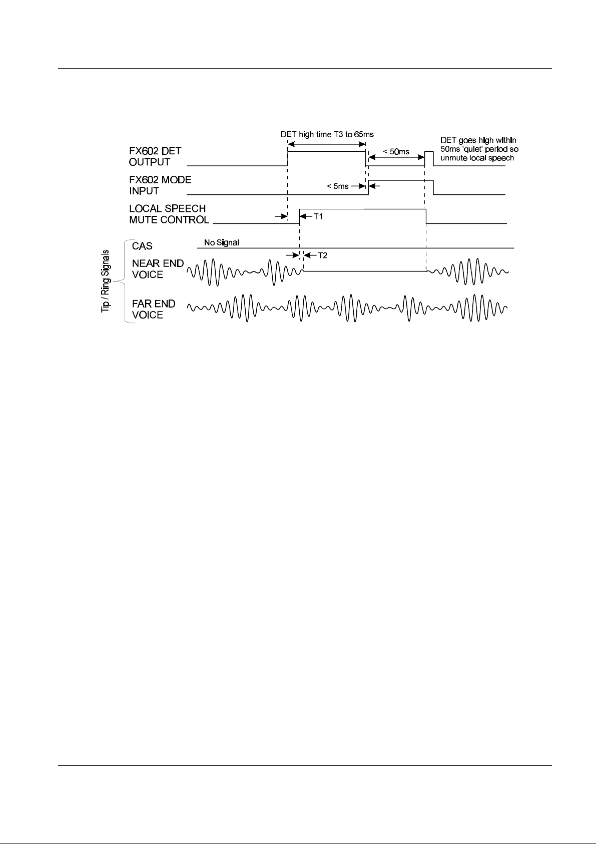
If the DET output is still high when timer reaches 65ms the signal is too long to be a valid CAS and
must have been caused by far end speech, so cancel the speech muting and go to the
WAIT_DET_LOW state.
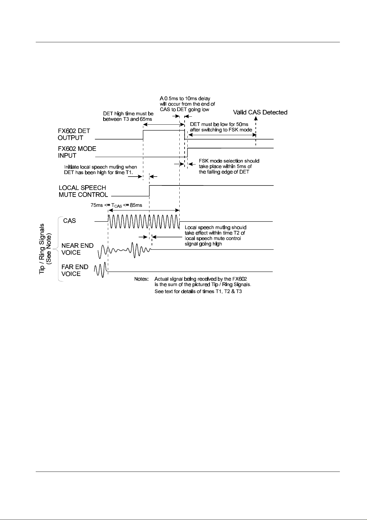
If the DET output goes low when the timer is between T3 and 65ms then it could be a valid CAS, in
which case it will be followed by a 'quiet' period (local speech being muted) so set the FX602 to FSK
Receive mode, reset the timer and go to the CONFIRM_QUIET state. These actions should take place
within 5ms of the DET output going low.
4. CONFIRM_QUIET state
During this state the energy present at the FX602's input after the end of the dual-tone detection is monitored
for up to 50ms using the FX602's FSK Level Detector circuits. If the received signal had been a valid CAS then
it would have been followed by a quiet period (the local speech being muted by this algorithm) whereas a false
signal caused by far end speech will contain additional energy in the following period.
If the DET output goes high before the timer has reached 50ms then remove local speech muting, set
the FX602 to Tone Alert Detect mode and return to the INITIAL state.
If the timer reaches 50ms then a valid CAS has been detected so go to the COMPLETE_CIDCW state.
5. COMPLETE_CIDCW state
This state handles the remaining CIDCW transaction functions e.g. determine that no near end extensions are
off hook, send a dtmf ACK signal to the Central Office, receive FSK Caller ID data stream, etc.
1996 Consumer Microcircuits Limited 18 D/602/5
Page 19

Calling Line Identifier FX602
Note that the 50ms monitoring period of the CONFIRM_QUIET state when added to the 0.5 to 10ms deresponse time of the FX602 in Tone Alert Detect mode and the 0 to 5ms delay in switching to FSK mode
results in a valid CAS detection occurring at between 50 and 65 ms after the end of the CAS, leaving at least
35ms for muting the local handset fully, testing for off-hook extensions and initiating the dtmf ACK transmission
while still meeting the 100ms specified for CIDCW from end of the dual-tone burst to the start of the ACK. See
also note 3 below.
When the transaction has been completed then remove speech muting, reset the timer, set the FX602
to Tone Alert Detect mode and return to the INITIAL state.
6. WAIT_DET_LOW state
This state is entered from the MEAS_DET_HIGH state when the FX602 DET output has been high for 65ms
i.e. for too long to be a valid CAS.
Wait for the DET output to go low then reset the timer and return to the INITIAL state.
Times T1, T2 & T3
The values given below have been selected to give an extremely low incidence of false CAS detections while
maintaining a high probability of decoding correct CIDCW initiation signals by taking advantage of the specific
profile of FX602's responses to typical speech and CAS signals. Two options are given, the choice being
determined principally by how easily the local speech can be muted.
a) When the CIDCW circuits are built into the telephone set so that locally generated speech can be
muted quickly and without injecting noise then it is recommended that:
T1 should be zero, i.e. muting should be initiated as soon as the FX602 DET output goes high.
T2, the time for local speech muting to take effect, should be as short as possible and in any
case not more than 5ms.
T3, the minimum length of a valid DET output high time, should be 15ms.
b) When the CIDCW circuits are housed in an adjunct box so that muting is only possible by interrupting
the 2-wire connection to the telephone set, then it is recommended that:
T1 should be 15ms i.e. speech muting should only be initiated after the DET output has been
high for 15ms.
T2, the time for speech muting to take effect, should be as short as possible and in any case
not more than 5ms.
T3, the minimum length of a valid DET output high time, should be equal to T1 plus T2 plus
10ms, i.e. between 25 and 30ms.
Option (b) reduces the frequency of short speech mutes by a factor of about 5 at the expense of a small
increase in the number of missed CAS signals.
1996 Consumer Microcircuits Limited 19 D/602/5
Page 20

Calling Line Identifier FX602
Notes:
1 When the FX602 is in Tone Alert Detect mode, the IRQN output will go low on the first high to low
transition of the DET output and will remain low until the FX602 is switched to FSK or Zero Power
mode. Accordingly the IRQN output should be ignored when looking for a CAS signal.
2. The task of monitoring the FX602's DET output during the CONFIRM_QUIET state may be eased by
noting that in FSK Receive mode any high pulses on the DET output will last for at least 8ms (or until
the mode is changed) so the signal need only be monitored more frequently than once every 8ms.
3. The actual duration of the '50ms' monitoring period is not critical but should be at least 30ms to allow
time for the FSK level detector to respond.
1996 Consumer Microcircuits Limited 20 D/602/5
Page 21
Calling Line Identifier FX602
Timing Diagrams
Figures 9d to 9g illustrate the CIDCW transaction initiation sequence for various cases.
Figure 9d : Valid CIDCW Transaction Initiation Sequence
1996 Consumer Microcircuits Limited 21 D/602/5
Page 22

Calling Line Identifier FX602
Figure 9e : Invalid CIDCW Transaction Initiation Sequence
(DET Output high for less than time T3)
Figure 9f : Invalid CIDCW Transaction Initiation Sequence
(DET Output high for more than 65ms)
1996 Consumer Microcircuits Limited 22 D/602/5
Page 23
Calling Line Identifier FX602
Figure 9g : Invalid CIDCW Transaction Initiation Sequence
(DET Output goes high during 50ms 'quiet' period)
1996 Consumer Microcircuits Limited 23 D/602/5
Page 24

Calling Line Identifier FX602
1.7 Performance Specification
1.7.1 Electrical Performance
Absolute Maximum Ratings
Exceeding these maximum ratings can result in damage to the device.
Min. Max. Units
Supply (VDD - VSS) -0.3 7.0 V
Voltage on any pin to V
Current into or out of V
SS
DD
and V
pins -30 +30 mA
SS
Current into or out of any other pin -20 +20 mA
D4 / P3 Packages Min. Max. Units
Total Allowable Power Dissipation at Tamb = 25°C 800 mW
... Derating 13 mW/°C
Storage Temperature -55 +125 °C
Operating Temperature -40 +85 °C
-0.3 V
+ 0.3 V
DD
Operating Limits
Correct operation of the device outside these limits is not implied.
Notes Min. Max. Units
Supply (VDD - VSS) 3.0 5.5 V
Operating Temperature -40 +85 °C
Xtal frequency 1 3.575965 3.583125 MHz
Notes: 1. A Xtal frequency of 3.579545MHz ±0.1% is required for correct Tone Alert and FSK
detection.
1996 Consumer Microcircuits Limited 24 D/602/5
Page 25

Calling Line Identifier FX602
µ
µ
Operating Characteristics
For the following conditions unless otherwise specified:
= 3.0V at Tamb = 25°C and V
V
DD
Xtal Frequency = 3.579545MHz
= 3.3V to 5.5V at Tamb = - 40 to +85°C,
DD
± 0.1%
0dBV corresponds to 1.0Vrms
Notes Min. Typ. Max. Units
DC Parameters
IDD (ZP input high) at VDD = 5.0V 1,2 1.0
(ZP input low) at VDD = 3.0V 1 0.5 1.0 mA
I
DD
(ZP input low) at V
I
DD
= 5.0V 1 1.0 2.0 mA
DD
Logic '1' input level (RXCK and XTAL inputs) 70% V
Logic '0' input level (RXCK and XTAL inputs) 30% V
Logic input leakage current (Vin = 0 to VDD),
-1.0 +1.0
excluding XTAL input
Output logic '1' level (l
Output logic '0' level (l
IRQN o/p 'off' state current (Vout = V
= 360µA) VDD - 0.4 V
OH
= 360µA) 0.4 V
OL
) 1.0 µA
DD
Schmitt Trigger input thresholds, see fig 10
High going (Vthi) 0.56V
DD
0.56V
DD
+ 0.6
Low going (Vtlo) 0.44V
DD
0.44V
DD
- 0.6
A
DD
DD
A
V
V
Tone Alert Detector
'Low' tone nominal frequency 2130 Hz
'High' tone nominal frequency 2750 Hz
Start of Tone Alert signal to DET high time
40 msec
(Fig. 6 Tton)
End of Tone Alert signal to DET and IRQN low
time (Fig 6 Ttoff) 0.5 10.0 msec
To ensure detection ; 3
'Low' tone frequency tolerance ±20 Hz
'High' tone frequency tolerance ±30 Hz
Level (total) 4 -40.0 -2.2 dBV
2750Hz tone level wrt
2130Hz tone level -7.0 +7.0 dB
Signal to Noise ratio 5 20.0 dB
Dual tone burst duration 75 msec
To ensure non-detection ; 6
'Low' tone frequency tolerance ±75 Hz
'High' tone frequency tolerance ±95 Hz
Level (total) 4 -46.0 dBV
Dual tone burst duration 25 msec
1996 Consumer Microcircuits Limited 25 D/602/5
Page 26

Calling Line Identifier FX602
Notes Min. Typ. Max. Units
FSK Receiver
Transmission rate 1188 1200 1212 Baud
V23 Mark (logical 1) frequency 1280 1300 1320 Hz
V23 Space (logical 0) frequency 2068 2100 2132 Hz
Bell202 Mark (logical 1) frequency 1188 1200 1212 Hz
Bell202 Space (logical 0) frequency 2178 2200 2222 Hz
Valid input level range 4 -40.0 -8.0 dBV
Acceptable twist (mark level wrt space level)
V23 -7.0 +7.0 dB
Bell202 -10.0 +10.0 dB
Acceptable Signal to Noise ratio
V23 5 20.0 dB
Bell202 5 30.0 dB
Level Detector 'on' threshold level 4 -40.0 dBV
Level Detector 'off' to 'on' time (Fig 4 Teon) 25.0 msec
Level Detector 'on' to 'off' time (Fig 4 Teoff) 8.0 msec
Input Signal Amplifier
Input impedance 7 10.0
M
Ω
Voltage gain 500 V/V
XTAL Input
'High' pulse width 8 100 ns
'Low' pulse width 8 100 ns
Notes: 1. At 25°C, not including any current drawn from the FX602 pins by external circuitry other than
X1, C1 and C2.
2. RD, MODE, RXCK inputs at V
, ZP input at VDD. See also Figure 11.
SS
3. All conditions must be met to ensure detection.
4. For V
as section 1.4. The internal threshold levels are proportional to V
= 5.0V with equal level tones and with the input signal amplifier external components
DD
. To cater for other supply
DD
voltages or different signal level ranges the voltage gain of the input signal amplifier should be
adjusted by selecting the appropriate external components as described in section 1.5
5. Flat noise in 300-3400Hz band for V23, 200 - 3200Hz for Bell202.
6. Meeting any of these conditions will ensure non-detection.
7. Open loop, small signal low frequency measurements.
8. Timing for an external input to the CLOCK/XTAL pin.
1996 Consumer Microcircuits Limited 26 D/602/5
Page 27

Calling Line Identifier FX602
µA
4
3.5
3
Vthi
2.5
Vin
2
1.5
1
Vtlo
0.5
0
3 3.5 4 4.5 5 5.5
V
DD
Figure 10 : Schmitt Trigger typical input voltage thresholds vs. V
10
1
DD
0.1
0.01
0.001
0.0001
-40 -30 -20 -10 0 10 20 30 40 50 60 70 80
Temperature
Figure 11 : Typical 'Zero Power' IDD vs. Temperature (VDD = 5.0V)
1996 Consumer Microcircuits Limited 27 D/602/5
Page 28

Calling Line Identifier FX602
1.7.2 Packaging
Figure 12 : 16-pin SOIC (D4) Mechanical Outline: Order as part no. FX602D4
Figure 13 : 16-pin DIL (P3) Mechanical Outline: Order as part no. FX602P3
Handling precautions: This product includes input protection, however, precautions should be taken to prevent
device damage from electro-static discharge. CML does not assume any responsibility for the use of any
circuitry described. No IPR or circuit patent licences are implied. CML reserves the right at any time without
notice to change the said circuitry and this product specification. CML has a policy of testing every product
shipped using calibrated test equipment to ensure compliance with this product specification. Specific testing
of all circuit parameters is not necessarily performed.
CONSUMER MICROCIRCUITS LIMITED
1 WHEATON ROAD Telephone: +44 1376 513833
WITHAM - ESSEX CM8 3TD - ENGLAND Telefax: +44 1376 518247
 Loading...