

Page 1
查询FX469DS供应商
CML Semiconductor Products
PRODUCT INFORMATION
FX469
Features
Selectable Data Rates
1200, 2400 and 4800 Baud
Full-Duplex FFSK
Rx and Tx Bandpass Filters
Clock Recovery and Carrier
Detect Facilities
Rx and Tx Enable Functions
TxGENERATOR
TxDATAI/P
TxENABLE
CLOCKRATE
XTAL/CLOCK
XTAL
1200/2400BAUDSELECT
4800BAUDSELECT
RxENABLE
RxSIGNALI/P
OSCILLATOR
RxFILTER
CLOCK
TxFILTER
DIVIDER
LIMITER LIMITER
f
..n
RETRIGGERABLE
MONOSTABLE
1200/2400/4800 Baud
FFSK Modem
Publication D/469/6 April 1998
Pin Selected Xtal/Clock Inputs
1.008MHz or 4.032MHz
Radio and General Applications
Data-Over-Radio
PMR and Cellular Signalling
Portable Data Terminals
Personal/Cordless Telephone
TxSIGNALO/P
TxSYNCO/P
V
DD
V
BIAS
V
SS
BANDPASSO/P
UNCLOCKED
DATAO/P
DIGITAL
FILTER
DATA
FILTER
FX469
RECTIFIER
DIGITAL
PLL
NOISEFILTER
RECTIFIER
S/N
COMPARATOR
CARRIERDETECTTIMECONSTANT
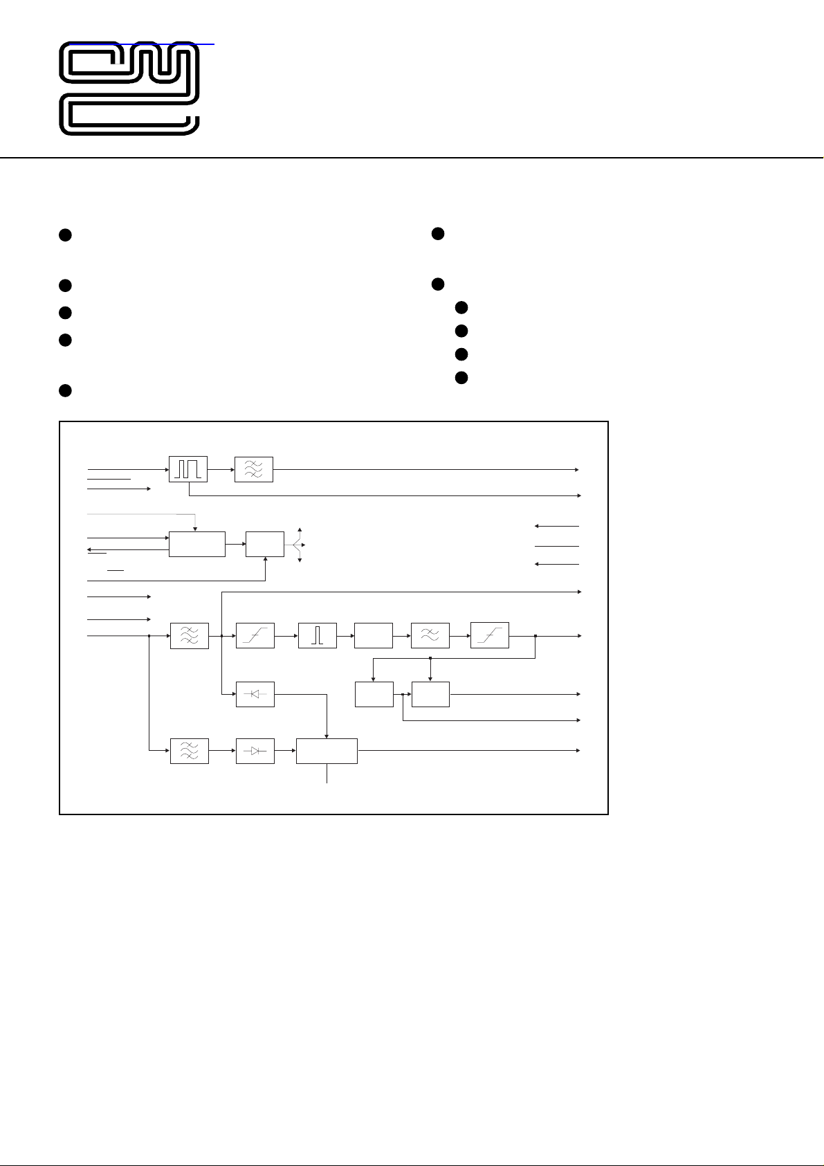
Fig.1 Functional Block Diagram
Brief DescriptionBrief Description
Brief Description
Brief DescriptionBrief Description
The FX469 is a single-chip CMOS LSI circuit which
operates as a full-duplex pin-selectable 1200, 2400 or
4800 baud FFSK Modem. The mark and space
frequencies are 1200/1800, 1200/2400 and 2400/4800
Hz respectively. Tone frequencies are phase
continuous; transitions occur at the zero crossing point.
Employing a common Xtal oscillator with a choice of
two clock frequencies (1.008MHz or 4.032MHz) to
provide baud-rate, transmit frequencies, and Rx and Tx
synchronization, the transmitter and receiver operate
entirely independently including individual section
powersave functions.
The FX469 includes on chip circuitry for Carrier Detect
and Rx Clock recovery, both of which are made
available as output pins.
CLOCKED
DATA
LATCH
CARRIERDETECTO/P
DATAO/P
RxSYNCO/P
Rx, Tx and Carrier Detect paths each contain a
bandpass filter to ensure the provision of optimum
signal conditions both in the modem and for the Tx
modulation circuitry.
The FX469 demonstrates a high sensitivity and
good bit-error-rate under adverse signal conditions;
the carrier detect time constant is set by an external
capacitor, whose value should be arranged as
required to further enhance this product's performance
in high noise environments.
This low-power device requires few external
components and is available in small outline plastic
(S.O.I.C) and cerdip DIL packages.
1
Page 2

Pin Number Function
FX469
DW
LG/LS
J/P6
1
1
1
Xtal/Clock : The input to the on-chip inverter, for use with either a 1.008MHz or a 4.032MHz
Xtal or external clock. Clock frequency selection is by the “Clock Rate” input pin. The
selection of this frequency will affect the operational Data Rate of this device. Refer to Baud
Selection information on the next page. Operation of any CML microcircuit without a Xtal or
clock input may cause device damage. To minimise damage in the event of a Xtal/drive
failure. it is recommended that the power rail (VDD) is fitted with a current limiting device
(resistor or fast-reaction fuse).
2
3
2
3
2
XtalN : Output of the on-chip inverter.
3
Tx Sync O/P : A squarewave, produced on-chip, to synchronize the input of logic data and
transmission of the FFSK signal (See Figure 4).
4
5
Tx Signal O/P : When the transmitter is enabled, this pin outputs the (140-step pseudo
5
sinewave) FFSK signal (See Figure 4).
With the transmitter disabled, this output is set to a high-impedance state.
5
6
7
8
Tx Data I/P : Serial logic data to be transmitted is input to this pin.
6
Tx EnableN : A logic ‘0’ will enable the transmitter (See Figure 4). A logic ‘1’ at this input will
7
put the transmitter into powersave whilst forcing “Tx Sync Out” to a logic ‘1’ and “Tx Signal
Out” to a high-impedance state. This pin is internally pulled to VDD.
7
9
Bandpass O/P : The output of the Rx Bandpass Filter. This output impedance is typically
8
10kW and may require buffering prior to use.
8
10
Rx Enable : The control of the Rx function. The control of other outputs is given below.
9
Rx Enable = Rx Function Clock Data O/P Carrier Detect Rx Sync Out
“1” = Enabled Enabled Enabled Enabled
“0” = Powersave “0” “0” 1” or “0”
V
9
11
10
: The output of the on-chip analogue bias circuitry. Held internally at VDD/2, this pin
BIAS
should be decoupled to VSS by a capacitor (C2). (See Figure 2.
This bias voltage is maintained under all powersave conditions.
10
12
11
VSS: Negative supply rail (GND).
2
Page 3
Pin Number Function
FX469
DW
LG/LS
J/P6
11
12
13
14
15
16
13
14
15
16
18
19
12
Unclocked Data O/P: The recovered asynchronous serial data output from the receiver.
13
Clocked Data O/P: The recovered synchronous serial data output from the receiver.
Data is latched out by the recovered clock, available at the “Rx Sync O/P,” (See Figure 5).
14
Carrier Detect O/P: When an FFSK signal is being received this output is a logic ‘1.’
15
Rx Signal I/P: The FFSK signal input for the receiver. This input should be coupled via a
capacitor, C3.
17
Rx Sync O/P: A flywheel squarewave output. This clock will synchronize to incoming Rx
FFSK data (See Figure 5).
16
1200/2400 Baud Select: A logic ‘1’ on this pin selects the 1200 baud option.
Tone frequencies are: one cycle of 1200Hz represents a logic ‘1,’ one-and-a-half cycles of
1800Hz represents a logic ‘0.’ A logic ‘0’ on this pin selects the 2400 baud option.
Tone frequencies are: one-half cycle of 1200Hz represents a logic ‘1,’ one cycle of 2400Hz
represents a logic ‘0.’ This function is also used, in part, to select the 4800 baud option. This
pin has an internal 1MW pullup resistor.
17
18
19
20
21
22
Operational Data Rate Configurations are illustrated in the table below.
Xtal/Clock Frequency 1.008MHz 4.032MHz
Clock Rate pin 0 0 1 1 1
1200/2400 Select pin 1 0 1 0 0
4800 Select pin 0 0 0 0 1
Baud Rate 1200 2400 1200 2400 4800
4800 Baud Select: A logic ‘1’ on this pin combined with a logic ‘0’ on the 1200/2400 Baud
18
Select pin will select the 4800 option (1MW pulldown resistor).
Tone frequencies are: one-half cycle of 2400Hz represents a logic ‘1,’ one cycle of 4800Hz
represents a logic ‘0.’ This state can only be achieved using a 4.032MHz Xtal input.
Clock Rate: A logic input to select and allow the use of either a 1.008MHz or 4.032MHz
19
Xtal/clock. Logic ‘1’ = 4.032MHz, logic ‘0’ = 1.008MHz. This input has an internal pulldown
resistor (1.008MHz).
Carrier Detect Time Constant : Part of the carrier detect integration function. The value of
20
C4 connected to this pin will affect the carrier detect response time and hence noise
performance (See Figure 2, Note 3).
20
24
4, 6, 17,
23
VDD: Positive supply rail. A single 5-volt supply is required.
22
No internal connection, do not use.
4,
21
3
Page 4

Application Information
V
DD
XTAL/CLOCK
R
1
X
1
C
C
1
7
Tx SYNC O/P
XTAL
Tx SIGNAL O/P
Tx DAT A I/P
V
DD
Tx ENABLE
BANDPASS O/P
C
6
C
2
Rx ENABLE
V
V
BIAS
SS
Component Value Tolerance
R
1
C
1
C
2
C
3
C
4
C
5
C
6
C
7
X
1
1.0MW ±10%
33.0pF
1.0µF ±20%
0.1µF
0.1µF ±10%
1.0µF ±20%
1.0µF
33.0pF
1.008MHz See
or ‘Clock-Rate’
4.032MHz Pin
Fig.2 External Components
1
2
3
4
5
6
7
8
9
10
11
FX469J
V
SS
C
5
SS
C
4
22
21
20
19
18
17
16
15
14
13
12
V
DD
CARRIER DETECT
TIME CONSTANT
V
CLOCK RATE
4800 BAUD SELECT
Rx SYNC O/P
1200/2400 BAUD SELECT
C
Rx SIGNAL I/P
3
CARRIER DETECT O/P
CLOCKED DATA O/P
UNCLOCKED DATA O/P
Notes
1. V
2. Use C
3. The value of C4 determines the Carrier Detect time
4. C7 reduces Xtal voltage overshoot. Refer to CML Xtal
may be decoupled to VSS and VDD using C2 and C
BIAS
when input signals are referenced to the V
input signals referenced to VSS, decouple V
pin. For
BIAS
BIAS
to V
using C2 only.
when input signals are referenced to VSS, to
5
decouple VDD.
constant. A long time constant results in improved noise
immunity but increased response time. C4 may be varied
to trade-off response time for noise immunity.
Application Note D/XT/2 December 1991.
6
SS
V
DD
MILLI-
AMMETER
Tx
DATA
Tx SYNC
I/P
FX469
TRANSMITTER
(components
as Fig. 2)
OSCILLOSCOPE
PREAMBLE &
PSEUDO-RANDOM
DATA
GENERATOR
Fig.3 Suggested FX469 Test Set-Up
V
SIGNAL
SS
Tx
O/P
BUFFER
(INTERFACE)
CIRCUIT
TRUE RMS
VOLTMETER
(with attenuator
5kHz BW noise gen)
4
TELEPHONE
CHANNEL
SIMULATOR
&
Rx
SIGNAL
I/P
TRUE RMS
VOLTMETER
V
DD
MILLI-
AMMETER
FX469
RECEIVER
(components
as Fig. 2)
V
SS
CLOCKED
DATA O/P
SYNC
CARRIER
DETECT
O/P
Rx
ERROR
DETECTOR
CARRIER
DETECT
O/P HIGH
DETECTOR
Page 5

Application InfApplication Inf
Application Inf
Application InfApplication Inf
Tx
ENABLE
Tx
SYNC
Tx DATA
DC = Don’t Care
DV = Data Valid
ormation ......ormation ......
ormation ......
ormation ......ormation ......
t
DSETDSET
DC
t
ESET
t
DH
DV
DC
t
TxD
t
TDR
DV
DC DC
DV
t
TDR
1200 BAUD
Tx OUTPUT
2400 BAUD
Tx OUTPUT
OPEN CIRCUIT
OPEN CIRCUIT
OPEN CIRCUIT
OPEN CIRCUIT
Fig.4 Transmitter Timing
Characteristics Note Min. Typ. Max. Unit
Tx Delay, Signal to Disable Time t
Data Set-Up Time t
Data Hold Time t
Tx Delay to O/P Time t
Tx Data Rate Period t
Rx Data Rate Period t
Undetermined State - - 2.0 µs
Internal Rx Delay t
ESET
DSET
DH
TxD
TDR
RDR
ID
1. Consider the Xtal/Clock tolerance.
2. All Tx timings are related to the Tx Sync Output.
3. 1200 baud example.
3 2.0 - 800 µs
1 2.0 - - µs
2.0 - - µs
- 1.2 - µs
3 - 833 - µs
3 800 - 865 µs
- 1.5 - ms
Rx
SIGNAL I/P
2400/4800 BAUD
Rx
SIGNAL I/P
1200 BAUD
Rx
SYNC O/P
(1200Hz)
CLOCKED
DAT A O/P
Fig.5 Rx Timing Diagram
LOGIC ’1’
1
0
1
0
t
t
RDR
LOGIC ’0’
ID
Undetermined
State
LOGIC ’1’ LOGIC ’0’
5
Page 6

Specification
Absolute Maximum Ratings
Exceeding the maximum rating can result in device damage. Operation of the device outside the operating limits is
not implied.
Supply voltage -0.3 to 7.0V
Input voltage at any pin (ref V
Sink/source current (supply pins) +/- 30mA
(other pins) +/- 20mA
Total device dissipation @ T
Derating 10mW/°C
Operating temperature range:FX469DW/LG/LS/P6 -30°C to +70°C (plastic)
Storage temperature range: FX469DW/LG/LS/P6 -40°C to +85°C (plastic)
Operating Limits
All device characteristics are measured under the following conditions unless otherwise specified:
V
= 5.0V, T
DD
Signal-to-Noise Ratio measured in the Bit-Rate Bandwidth Baud Rate = 1200 baud.
= 25°C. Audio Level 0dB ref: = 300mVrms. Xtal/Clock = 4.032MHz.
AMB
= 0V) -0.3 to (V
SS
25°C 800mW Max.
AMB
+ 0.3V)
DD
FX469J -30°C to +85°C (cerdip)
FX469J -55°C to +125°C (cerdip)
Characteristics See Note Min. Typ. Max. Unit
Static Values
Supply Voltage 4.5 5.0 5.5 V
Supply CurrentRx EnabledTx Disabled - 3.6 - mA
Rx and Tx Enabled - 4.5 - mA
Rx and Tx Disabled - 650 - µA
Logic ‘1‘ Level 1 4.0 - - V
Logic ‘0’ Level 1 - - 1.0 V
Digital Output Impedance - 4.0 - kW
Analogue and Digital Input Impedance 100 - - kW
Tx Output Impedance - 0.6 1.0 kW
On-Chip Xtal Oscillator
R
IN
R
OUT
Inverter d.c. Voltage Gain 10.0 - 20.0 V/V
Gain Bandwidth Product 4.1 - - MHz
Xtal Frequency 2 - 1.008 - MHz
Xtal Frequency 2 - 4.032 - MHz
Dynamic Values
Receiver
Signal Input Dynamic RangeSNR = 50dB 3, 4 100 230 1000 mVrms
Bit Error Rate SNR = 12dB 4
1200 Baud - 2.5 - 10
2400 Baud - 1.5 - 10
4800 Baud - 1.5 - 10
SNR = 20dB 4
1200/2400/4800 Baud - <1.0 - 10
10.0 - - MW
5.0 - 15.0 kW
4
3
3
8
Receiver SynchronizationSNR =12dB 7
Probability of Bit 16 Being Correct - 0.995 -
Carrier Detect 5, 10
Sensitivity 7, 8 - - 150 mVrms
Probabilty of C.D. Being High
After Bit 16 SNR = 12dB 5, 9 0.995
0dB Noise No Signal 9 0.05
6
Page 7

Specification ......
Characteristics See Note Min. Typ. Max. Unit
Transmitter Output
Tx Output Level - 775 - mVrms
Output Level Variation
1200/1800Hz or 1200/2400Hz or 2400/4800Hz 0 - ±1.0 dB
Output Distortion - 3.0 5.0 %
3rd Harmonic Distortion - 2.0 3.0 %
Logic ‘1’ Carrier Frequency 1200 Baud 6 - 1200 - Hz
2400 Baud 6 - 1200 - Hz
4800 Baud 6 - 2400 - Hz
Logic ‘0’ Carrier Frequency 1200 Baud 6 - 1800 - Hz
2400 Baud 6 - 2400 - Hz
4800 Baud 6 - 4800 - Hz
Isochronous Distortion
1200Hz - 1800Hz/1800Hz - 1200Hz - 25.0 40.0 µs
1200Hz - 2400Hz/2400Hz - 1200Hz - 20.0 30.0 µs
2400Hz - 4800Hz/4800Hz - 2400Hz - 10.0 20µs
Notes
1. With reference to VDD = 5.0 volts.
2. Xtal frequency, type and tolerance depends upon system requirements.
3. See Figure 5 (variation of BER with Input Signal Level).
4. SNR = Signal-to-Noise Ratio in the Bit-Rate Bandwidth.
5. See Figure 2.
6. Dependent upon Xtal tolerance.
7. 10101010101 ...01 pattern.
8. Measured with a 150mVrms input signal (no noise); 1200/2400 baud operation.
9. Reference (0dB) level for C.D. probability measurements is 230mVrms.
10.For 1200 and 2400 baud operation only; when operating at 4800 baud the Carrier Detect output
should be ignored.
-1
1x10
*
BITRATEBANDWIDTH
-2
1x10
10dB SNR
12dB SNR
*
*
-3
1x10
BIT ERROR RA TE
1x10
1x10
-4
-5
50
20dB SNR
*
100
150
Fig.6 Typical Variation of Bit Error Rate with Input Level
200
250
300
INPUTSIGNALLEVEL(mVrms)
500
700
800
7
Page 8

Application Information
)
NOT TO SCALE
Max. Body Length 27.38mm
Max. Body Width 9.75mm
2x10
10
10
10
BIT ERROR RATE (log scale)
10
-2
-2
-3
-4
8
6
4
2
-5
0
IDEAL COHERENT FFSK
34 5
2
1
Fig.7 Rx Bit-Error-Rate vs Signal-to-Noise Ratio
FX469
78
6
13
9
10 11
12
14 15 16
SNR(dB)BIT RATE BANDWIDTH(lin scale
Package Outlines
The FX469 is available in the package styles outlined
below. Mechanical package diagrams and specifications
are detailed in Section 10 of this document.
Pin 1 identification marking is shown on the relevant
diagram and pins on all package styles number
anti-clockwise when viewed from the top.
FX469DWFX469DW
FX469DW 20-pin plastic S.O.I.C. (D3)
FX469DWFX469DW
NOT TO SCALE
Handling Precautions
The FX469 is a CMOS LSI circuit which includes input
protection. However precautions should be taken to
prevent static discharges which may cause damage.
FX469JFX469J
FX469J 22-pin cerdip DIL (J3)
FX469JFX469J
Max. Body Length 12.95mm
Max. Body Width 7.59mm
8
Page 9

Package Outlines ......
FX469LGFX469LG
FX469LG 24-pin quad plastic encapsulated
FX469LGFX469LG
bent and cropped (L1)
NOT TO SCALE
Max. Body Length 10.25mm
Max. Body Width 10.25mm
FX469LSFX469LS
FX469LS 24-lead plastic leaded chip
FX469LSFX469LS
carrier (L2)
NOT TO SCALE
Max. Body Length 10.40mm
Max. Body Width 10.40mm
Ordering Information
FX469DW 20-pin surface mount S.O.I.C.
FX469J 22-pin cerdip DIL
FX469LGFX469LG
FX469LG 24-pin quad plastic encapsulated
FX469LGFX469LG
bent and cropped
(L1)
FX469LSFX469LS
FX469LS 24-lead plastic leaded chip carrier
FX469LSFX469LS
(L2)
FX469P6FX469P6
FX469P6 22-pin plastic DIL
FX469P6FX469P6
FX469P6FX469P6
FX469P6 22-pin plastic DIL
FX469P6FX469P6
NOT TO SCALE
Max. Body Length 27.94mm
Max. Body Width 9.14mm
CML does not assume any responsibility for the use of any circuitry described. No circuit patent licences are implied
and CML reserves the right at any time without notice to change the said circuitry.
9
 Loading...