

Page 1
Any and all SANYO products described or contained herein do not have specifications that can handle
applications that require extremely high levels of reliability, such as life-support systems, aircraft’s
control systems, or other applications whose failure can be reasonably expected to result in serious
physical and/or material damage. Consult with your SANYO representative nearest you before using
any SANYO products described or contained herein in such applications.
SANYO assumes no responsibility for equipment failures that result from using products at values that
exceed, even momentarily, rated values (such as maximum ratings, operating condition ranges,or other
parameters) listed in products specifications of any and all SANYO products described or contained
herein.
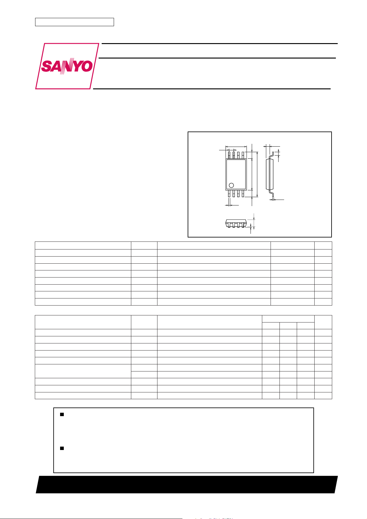
N-Channel Silicon MOSFET
Load Switching Applications
Ordering number:ENN6267
FTD2014
SANYO Electric Co.,Ltd. Semiconductor Company
TOKYO OFFICE Tokyo Bldg., 1-10, 1 Chome, Ueno, Taito-ku, TOKYO, 110-8534 JAPAN
6.4
3.0
0.425
0.65
4.5 0.95
(0.95)
0.5
0.125
85
14
0.25
1.0
0.1
Features
· Low ON resistance.
· 2.5V drive.
· Mounting height 1.1mm.
· Composite type, facilitating high-density mounting.
Specifications
Absolute Maximum Ratings at Ta = 25˚C
retemaraPlobmySsnoitidnoCsgnitaRtinU
egatloVecruoS-ot-niarDV
egatloVecruoS-ot-etaGV
)CD(tnerruCniarDI
)eslup(tnerruCniarDI
noitapissiDrewoPelbawollAP
noitapissiDlatoTP
erutarepmeTlennahChcT 051
erutarepmeTegarotSgtsT 051+ot55–
Electrical Characteristics at Ta = 25˚C
retemaraPlobmySsnoitidnoC
egatloVnwodkaerBecruoS-ot-niarDV
tnerruCniarDegatloVetaG-oreZI
tnerruCegakaeLecruoS-ot-etaGI
egatloVffotuCV
ecnattimdArefsnarTdrawroF|sfy|VSDI,V01=
ecnatsiseRetatS-nOecruoS-ot-niarDcitatS
ecnaticapaCtupnIssiCV
ecnaticapaCtuptuOssoCV
ecnaticapaCrefsnarTesreveRssrCV
Marking : D2014 Continued on next page.
SSD
SSG
D
R
R
WP ≤ elcycytud,sµ01 ≤ %102A
PD
Mounted on a ceramic board (1000mm2×0.8mm) 1unit
D
Mounted on a ceramic board (1000mm
T
I
SSD)RB(
D
V
SSD
SSG
)ffo(SG
1IDV,A4=
)no(SD
2IDV,A2=
)no(SD
SD
V
SG
V
SD
SD
SD
SD
Package Dimensions
unit:mm
2155A
[FTD2014]
1 : Drain1
2 : Source1
3 : Source1
4 : Gate1
5 : Gate2
6 : Source2
7 : Source2
8 : Drain2
SANYO : TSSOP8
02V
01±V
4A
sgnitaR
8.0W
3.1W
˚C
˚C
tinU
2
×0.8mm)
nimpytxam
V,Am1=
0=02V
SG
V,V02=
0=1Aµ
SG
V,V8±=
0=01±Aµ
SD
I,V01=
Am1=4.03.1V
D
A4=701S
D
V4=2324mΩ
SG
V5.2=2495mΩ
SG
zHM1=f,V01=007Fp
zHM1=f,V01=002Fp
zHM1=f,V01=051Fp
21400TS (KOTO) TA-2166 No.6267–1/4
Page 2
FTD2014
Continued from preceding page.
retemaraPlobmySsnoitidnoC
emiTyaleDNO-nruTt
emiTesiRt
emiTyaleDFFO-nruTt
emiTllaFt
egrahCetaGlatoTgQ
egrahCecruoS-ot-etaGsgQ 4.1Cn
egrahC"relliM"niarD-ot-etaGdgQ 2.3Cn
egatloVdrawroFedoiDV
)no(d
r
)ffo(d
f
V
I
DS
S
V,V01=
SD
SG
V,A4=
0=58.02.1V
SG
Switching Time Test Circuit Electrical Connection
VDD=10V
V
IN
4V
0V
PW=10µs
D.C.≤1%
V
IN
G
D
ID=4A
RL=2.5Ω
V
OUT
tiucriCtseTdeificepSeeS41sn
tiucriCtseTdeificepSeeS031sn
tiucriCtseTdeificepSeeS38sn
tiucriCtseTdeificepSeeS011sn
I,V01=
A4=
D
D2 G2S2 S2
sgnitaR
nimpytxam
42Cn
tinU
P.G
50Ω
12
4.0V
10
2.5V
3.5V
ID -- V
2.0V
FTD2014
S
DS
Ta=25°C
3.0V
8
–A
D
6
1.5V
4
Drain Current, I
2
VGS=1.0V
0
02.0
90
80
mΩ
70
–
60
DS(on)
50
40
30
20
10
Static Drain-to-Source
On-State Resistance, R
0
0.5 1.0 1.5 2.5 3.0
Drain-to-Source Voltage, VDS –V
RDS(on) -- V
GS
4A
ID=2A
2406108
Gate-to-Source Voltage, VGS –V
IT00425
Ta=25°C
IT00427
D1 G1
S1 S1
12
VDS=10V
10
8
–A
D
6
4
Drain Current, I
2
0
0.2 0.6 1.61.00.8
0
0.4 1.41.2 1.8 2.0
Gate-to-Source Voltage, VGS –V
60
50
mΩ
–
40
DS(on)
30
20
10
Static Drain-to-Source
On-State Resistance, R
0
--2 5--5 0
(Top view)
I
-- V
D
25°C
GS
Ta=75°C
--25°C
RDS(on) -- Ta
=2.5V
GS
=2A, V
I
D
=4.0V
GS
=4A, V
I
D
0
Ambient Temperature, Ta – °C
IT00426
150125100755025
IT00428
No.6267-2/4
Page 3

100
7
5
|–S
fs
3
2
10
7
5
3
2
|yfs |-I
25°C
D
°C
Ta=--25
75°C
Forward Transfer Admittance, | y
1.0
23 57 23 57
Drain Current, ID–A
10000
1000
100
Ciss, Coss, Crss – pF
Ciss, Coss, Crss -- V
7
5
3
2
7
5
3
2
7
5
3
2
10
0
Ciss
Coss
Crss
624 8 1410 12 16
DS
Drain-to-Source Voltage, VDS–V
td(off)
r
SW Time -- I
td(on)
1000
7
5
3
2
100
7
5
3
2
10
7
5
Switching Time, SW Time – ns
3
2
1.0
0.1 1.0 10
t
D
23 5723 57
Drain Current, ID–A
P
-- Ta
1.4
1.2
–W
D
1.0
0.8
Mounted on a ceramic board (1000mm2×0.8mm)
D
Total Dissipation
VDS=10V
IT00429
f=1MHz
18
IT00431
VDD=10V
VGS=4V
t
IT00433
FTD2014
100.1 1.0
20
f
Ta=75°C
IF -- V
25°C
--25°C
0.5 0.7 0.8 0.9 1.0 1.10.2
100
10
–A
F
1.0
0.1
Forward Current, I
0.01
0.001
7
5
3
2
7
5
3
2
7
5
3
2
7
5
3
2
7
5
3
2
0.3 0.6 1.20.4
Diode Forward Voltage, VSD–V
V
-- Qg
10
–V
GS
Gate-to-Source Voltage, V
VDS=10V
9
ID=4A
8
7
6
5
4
3
2
1
0
5252015100
GS
Total Gate Charge, Qg – nC
100
7
5
3
I
DP
2
10
7
I
D
5
–A
3
D
2
1.0
7
5
3
Operation in this
2
area is limited by RDS(on)
Drain Current, I
0.1
7
5
Ta=25˚C
3
1 pulse, 1 unit
2
Mounted on a ceramic board (1000mm2×0.8mm)
0.01
0.01
0.1 1.0 10010
Drain-to-Source Voltage, VDS–V
A S O
DC operation
SD
100ms
<100
10ms
VGS=0
IT00430
IT00432
µs
1ms
23 7523 7523 7523 75
IT00434
0.6
0.4
0.2
1 unit
Allowable Power Dissipation, P
0
0 80 160
10020 40 60 120 140
Ambient Temperature, Ta – °C
IT00435
No.6267-3/4
Page 4
FTD2014
Specifications of any and all SANYO products described or contained herein stipulate the performance,
characteristics, and functions of the described products in the independent state, and are not guarantees
of the performance, characteristics, and functions of the described products as mounted in the customer's
products or equipment. To verify symptoms and states that cannot be evaluated in an independent device,
the customer should always evaluate and test devices mounted in the customer's products or equipment.
SANYO Electric Co., Ltd. strives to supply high-quality high-reliability products. However, any and all
semiconductor products fail with some probability. It is possible that these probabilistic failures could
give rise to accidents or events that could endanger human lives, that could give rise to smoke or fire,
or that could cause damage to other property. When designing equipment, adopt safety measures so
that these kinds of accidents or events cannot occur. Such measures include but are not limited to protective
circuits and error prevention circuits for safe design, redundant design, and structural design.
In the event that any or all SANYO products(including technical data,services) described or
contained herein are controlled under any of applicable local export control laws and regulations,
such products must not be exported without obtaining the export license from the authorities
concerned in accordance with the above law.
No part of this publication may be reproduced or transmitted in any form or by any means, electronic or
mechanical, including photocopying and recording, or any information storage or retrieval system,
or otherwise, without the prior written permission of SANYO Electric Co. , Ltd.
Any and all information described or contained herein are subject to change without notice due to
product/technology improvement, etc. When designing equipment, refer to the "Delivery Specification"
for the SANYO product that you intend to use.
Information (including circuit diagrams and circuit parameters) herein is for example only ; it is not
guaranteed for volume production. SANYO believes information herein is accurate and reliable, but
no guarantees are made or implied regarding its use or any infringements of intellectual property rights
or other rights of third parties.
This catalog provides information as of February, 2000. Specifications and information herein are subject
to change without notice.
PS No.6267-4/4
 Loading...