

Page 1
SANYO Electric Co.,Ltd. Semiconductor Bussiness Headquarters
TOKYO OFFICE, Tokyo Bldg., 1-10 , Chome, Ueno, Taito-ku, TOKYO, 110-8534 JAPAN
Ordering number:EN5263
FP502
N-Channel Silicon MOSFET
Silicon Schottky Barrier Diode
DC-DC Converter Applications
Features
· Composite type with a high-speed N-channel
MOSFET and a low-forward voltage Schottky
barrier diode contained in the PCP4 package, saving
the mount space greatly.
Specifications
Absolute Maximum Ratings at Ta = 25˚C
retemaraPlobmySsnoitidnoCsgnitaRtinU
noitapissiDrewoPelbawollA
erutarepmeTegarotSgtsT 051+ot55–
]kcolbSOM[
egatloVecruoS-ot-niarDV
egatloVecruoS-ot-etaGV
)CD(tnerruCniarDI
)esluP(tnerruCniarDI
erutarepmeTlennahChcT 051
]kcolbedoiD[
tnerruCdeifitceRegarevAI
P
D
P
D
SSD
SSG
D
PD
O
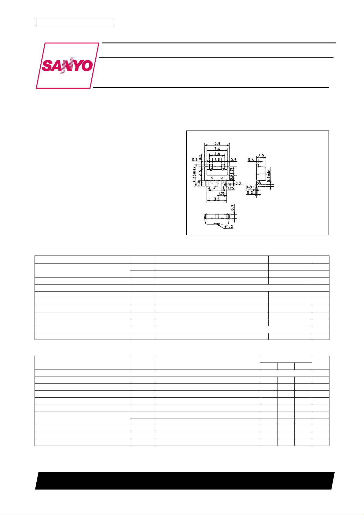
Package Dimensions
unit:mm
2132
[FP502]
Tc=25˚C, 1 unit
Mounted on ceramic board (250mm2×0.8mm) 1 unit
PW≤10µs, duty cycle ≤1%
1:Source, Anode
2:Common (Drain,
Cathode)
3:Source, Anode
4Common (Drain,
Cathode)
5:Gate
6:Common (Drain,
Cathode)
7:Common (Drain,
Cathode)
SANYO:PCP4
(Bottom view)
5.3W
5.1W
˚C
11V
01±V
2A
8A
˚C
005Am
Electrical Characteristics at Ta=25˚C
retemaraPlobmySsnotidnoC
]kcolbSOM[
egatloVnwodkaerBS-DV
tnerruCniarDegatloVetaG-oreZI
tnerruCegakaeLecruoS-ot-etaGI
egatloVffotuCV
ecnattimdArefsnarTdrawroFY|sf|VSDI,V01=
ecnatsiseRetatS-NOecruoS-ot-niarDcitatS
R
R
ecnaticapaCtupnIssiCV
ecnaticapaCtuptuOssoCV
ecnaticapaCrefsnarTesreveRssrCV
I
SSD)RB(
V
SSD
V
SSG
V
)ffo(SG
I
)no(SD
I
)no(SD
V,Am1=
D
SD
SG
SD
D
D
SD
SD
SD
0=11V
SG
V,V4.01=
0=004Aµ
SG
V,V8±=
0=01±Aµ
SD
I,V01=
Am1=0.10.4V
D
A1=2.12.2S
D
V,A1=
V01=041002mΩ
SG
V,Am005=
V4=002023mΩ
SG
zHM1=f,V01=051Fp
ZHN1=f,V01=002Fp
zHM1=f,V01=54Fp
52098HA(KT) 71096YK (KOTO) TA-0623 No.5263-1/4
nimpytxam
sgnitaR
tinU
Continued on next page.
Page 2
FP502
Continued from preceding page.
retemaraPlobmySsnotidnoC
]kcolbSOM[
emiTyaleDNO-nruTt
emiTesiRt
emiTyaleDFFO-nruTt
emiTllaFt
]kcolbedoiD[
egatloVdrawroF
emiTyrevoceResreveRt
)no(d
r
)ffo(d
f
V
I
F
rr
Am005=4.054.0V
F
I
F
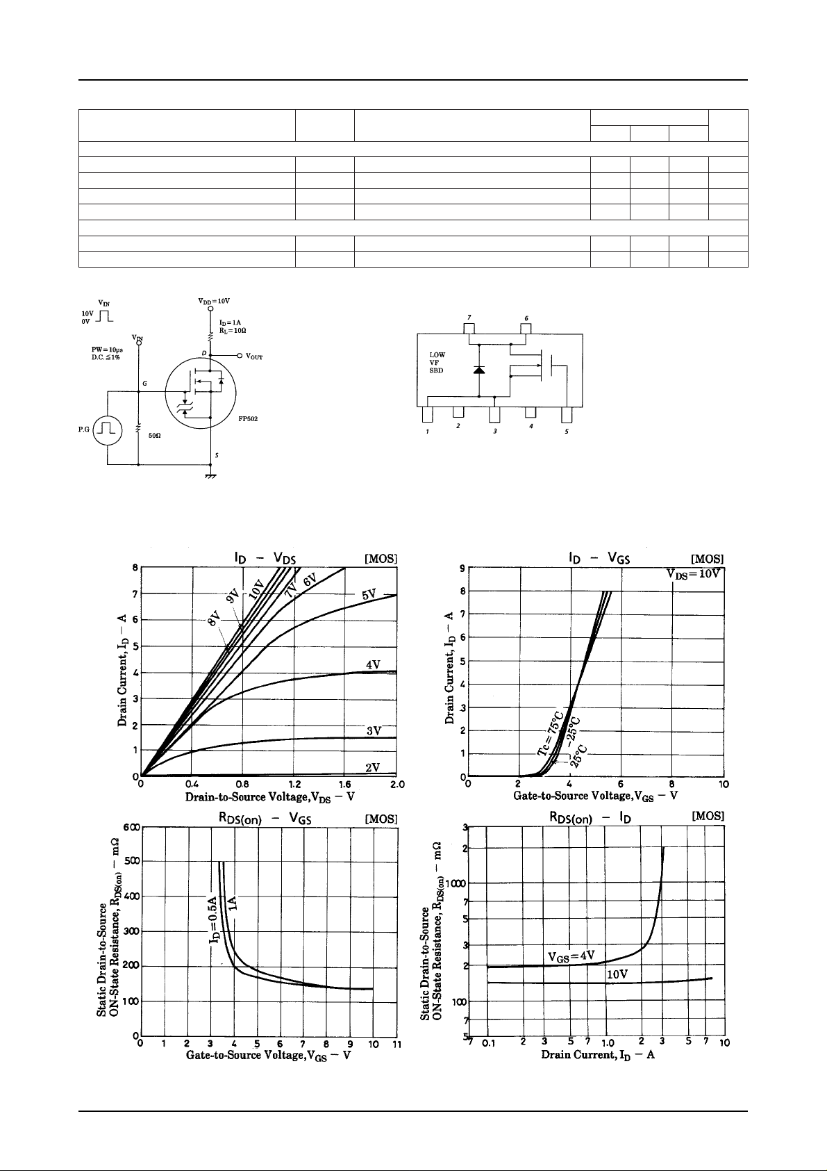
Switching Time Test Circuit Electrical Connection
.tiucriCtseTdeificepseeS01sn
.tiucriCtseTdeificepseeS52sn
.tiucriCtseTdeificepseeS52sn
.tiucriCtseTdeificepseeS02sn
sµ/A05=td/id,Am005=0203sn
sgnitaR
nimpytxam
1:Source, Anode
2:Common (Drain, Cathode)
3:Source, Anode
4Common (Drain, Cathode)
5:Gate
6:Common (Drain, Cathode)
7:Common (Drain, Cathode)
(Top view)
tinU
No.5263-2/4
Page 3

FP502
No.5263-3/4
Page 4

FP502
No products described or contained herein are intended for use in surgical implants, life-support systems,
aerospace equipment, nuclear power control systems, vehicles, disaster/crime-prevention equipment and
the like, the failure of which may directly or indirectly cause injury, death or property loss.
Anyone purchasing any products described or contained herein for an above-mentioned use shall:
Accept full responsibility and indemnify and defend SANYO ELECTRIC CO., LTD., its affiliates,
subsidiaries and distributors and all their officers and employees, jointly and severally, against any
and all claims and litigation and all damages, cost and expenses associated with such use:
Not impose any responsibilty for any fault or negligence which may be cited in any such claim or
litigation on SANYO ELECTRIC CO., LTD., its affiliates, subsidiaries and distributors or any of
their officers and employees jointly or severally.
Information (including circuit diagrams and circuit parameters) herein is for example only; it is not guarant-
eed for volume production. SANYO believes information herein is accurate and reliable, but no guarantees
are made or implied regarding its use or any infringements of intellectual property rights or other rights of
third parties.
This catalog provides information as of May, 1998. Specifications and information herein are subject to
change without notice.
PS No.5263-4/4
 Loading...