

Page 1
SANYO Electric Co.,Ltd. Semiconductor Bussiness Headquaters
TOKYO OFFICE Tokyo Bldg., 1-10, 1 Chome, Ueno, Taito-ku, TOKYO, 110-8534 JAPAN
N-Channel MOS Silicon FET
Very High-Speed
Switching Applications
Ordering number:EN4632
FP401
Features
· Low ON resistance.
· Very high-speed switching.
· Composite type with 2 low-voltage-drive N-channel
MOSFETs facilitating high-density mounting.
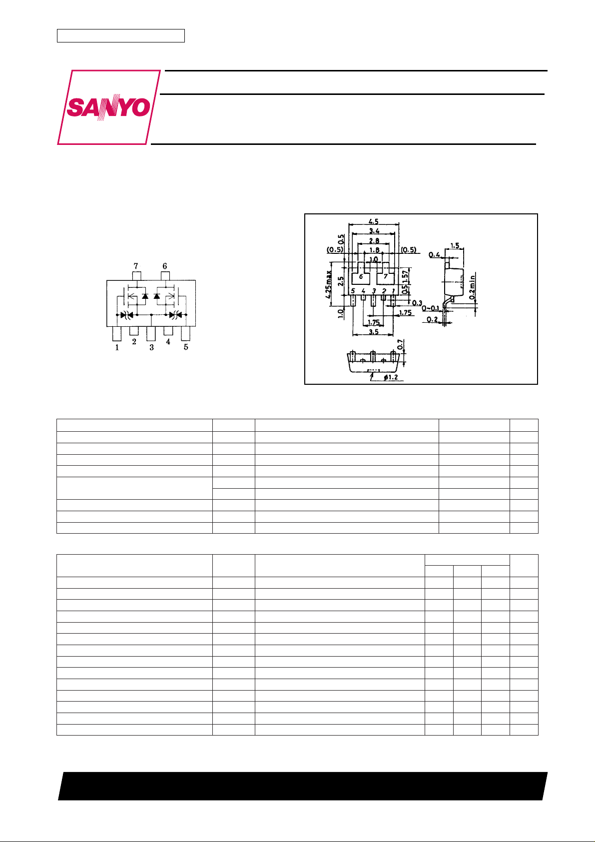
Electrical Connection
1:Gate
2:Drain
3:Source
4:Drain
5:Gate
6:Drain
7:Drain
Package Dimensions
unit:mm
2102A
[FP401]
1:Gate
2:Drain
3:Source
4:Drain
5:Gate
6:Drain
7:Drain
(Top view)
Specifications
Absolute Maximum Ratings at Ta = 25˚C
retemaraPlobmySsnoitidnoCsgnitaRtinU
egatloVecruoS-ot-niarDV
egatloVecruoS-ot-etaGV
)CD(tnerruCniarDI
)esluP(tnerruCniarDI
noitapissiDrewoPelbawollA
noitapissiDrewoPlatoTP
erutarepmeTlennahChcT 051
erutarepmeTegarotSgtsT 051+ot55–
Electrical Characteristics at Ta=25˚C
retemaraPlobmySsnotidnoC
egatloVnwodkaerBS-DV
tnerruCniarDegatloVetaGoreZI
tnerruCegakaeLecruoS-ot-etaGI
egatloVffotuCV
ecnattimdArefsnarTdrawroF|sfY|VSDI,V01=
ecnatsiseRetatS-NOecruoS-ot-niarDcitatSR
ecnaticapaCtupnIssiCV
ecnaticapaCtuptuOssoCV
ecnaticapaCrefsnarTesreveRssrCV
emiTyaleDNO-nruTt
emiTesiRt
emiTyaleDFFO-nruTt
emiTllaFt
egatloVdrawroFedoiDV
Marking:401
SSD
SSG
D
PW≤10µs, duty cycle ≤1%
PD
P
Tc=25˚C, 1 unit
D
Mounted on ceramic board (250mm2×0.8mm) 1 unit
P
D
Mounted on ceramic board (250mm2×0.8mm)
T
I
V,Am1=
SSD)RB(
D
V
SSD
SSG
r
f
DS
SD
V
SG
V
)ffo(SG
SD
I
)no(SD
D
SD
SD
SD
)no(d
)ffo(d
I
S
0=052V
SG
V,V052=
0=001Aµ
SG
V,V81±=
0=01±Aµ
SD
I,V01=
Am1=5.15.2V
D
Am002=072004Sm
D
V,Am002=
V01=821
SG
zHM1=f,V02=73Fp
zHM1=f,V02=01Fp
zHM1=f,V02=4Fp
tiucriCtseTdeificepseeS01sn
tiucriCtseTdeificepseeS01sn
tiucriCtseTdeificepseeS53sn
tiucriCtseTdeificepseeS54sn
V,Am004=
0=0.1V
SG
SANYO:PCP5
(Bottom view)
sgnitaR
nimpytxam
052V
02±V
004Am
6.1A
0.2W
8.0W
1.1W
˚C
˚C
tinU
Ω
52098HA (KT)/82494MT (KOTO) BX-0301 No.4632-1/3
Page 2
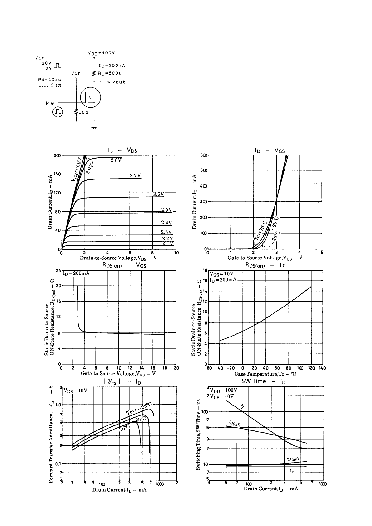
Switching Time Test Circuit
FP401
No.4632-2/3
Page 3

FP401
No products described or contained herein are intended for use in surgical implants, life-support systems,
aerospace equipment, nuclear power control systems, vehicles, disaster/crime-prevention equipment and
the like, the failure of which may directly or indirectly cause injury, death or property loss.
Anyone purchasing any products described or contained herein for an above-mentioned use shall:
Accept full responsibility and indemnify and defend SANYO ELECTRIC CO., LTD., its affiliates,
subsidiaries and distributors and all their officers and employees, jointly and severally, against any
and all claims and litigation and all damages, cost and expenses associated with such use:
Not impose any responsibilty for any fault or negligence which may be cited in any such claim or
litigation on SANYO ELECTRIC CO., LTD., its affiliates, subsidiaries and distributors or any of
their officers and employees jointly or severally.
Information (including circuit diagrams and circuit parameters) herein is for example only; it is not guaranteed for volume production. SANYO believes information herein is accurate and reliable, but no guarantees
are made or implied regarding its use or any infringements of intellectual property rights or other rights of
third parties.
This catalog provides information as of May, 1998. Specifications and information herein are subject to
change without notice.
PS No.4632-3/3
 Loading...