

Page 1
SANYO Electric Co.,Ltd. Semiconductor Bussiness Headquaters
TOKYO OFFICE Tokyo Bldg., 1-10, 1 Chome, Ueno, Taito-ku, TOKYO, 110-8534 JAPAN
TR:NPN Epitaxial Planar Silicon Transistor
SBD:Schottky Barrier Diode
DC-DC Converter Applications
Ordering number:EN4539
FP301
Features
· Composite type with 2 devices (NPN transistor and
Schottoky barrier diode) contained in one package,
facilitating high-density mounting.
· The FP301 is formed with a chip being equivalent to
the 2SD1621 and a chip being equivalent to the
SB07-03C placed in one package.
Specifications
Absolute Maximum Ratings at Ta = 25˚C
retemaraPlobmySsnoitidnoCsgnitaRtinU
]RT[
egatloVesaB-ot-rotcelloCV
egatloVrettimE-ot-rotcelloCV
egatloVesaB-ot-rettimEV
tnerruCrotcelloCI
)esluP(tnerruCrotcelloCI
tnerruCesaBI
noitapissiDrotcelloCP
erutarepmeTnoitcnuJjT 051
]DBS[
egatloVesreveRkaePevititepeRV
egatloVegruSesreveRkaePevititeper-noNV
tnerruCdeifitceRegarevAI
tnerruCdrawroFegruSI
erutarepmeTnoitcnuJjT 521+ot55–
erutarepmeTegarotSgtsT 521+ot55–
OBC
OEC
OBE
C
PC
B
Mounted on ceramic board (250mm
C
MRR
MSR
O
MSF
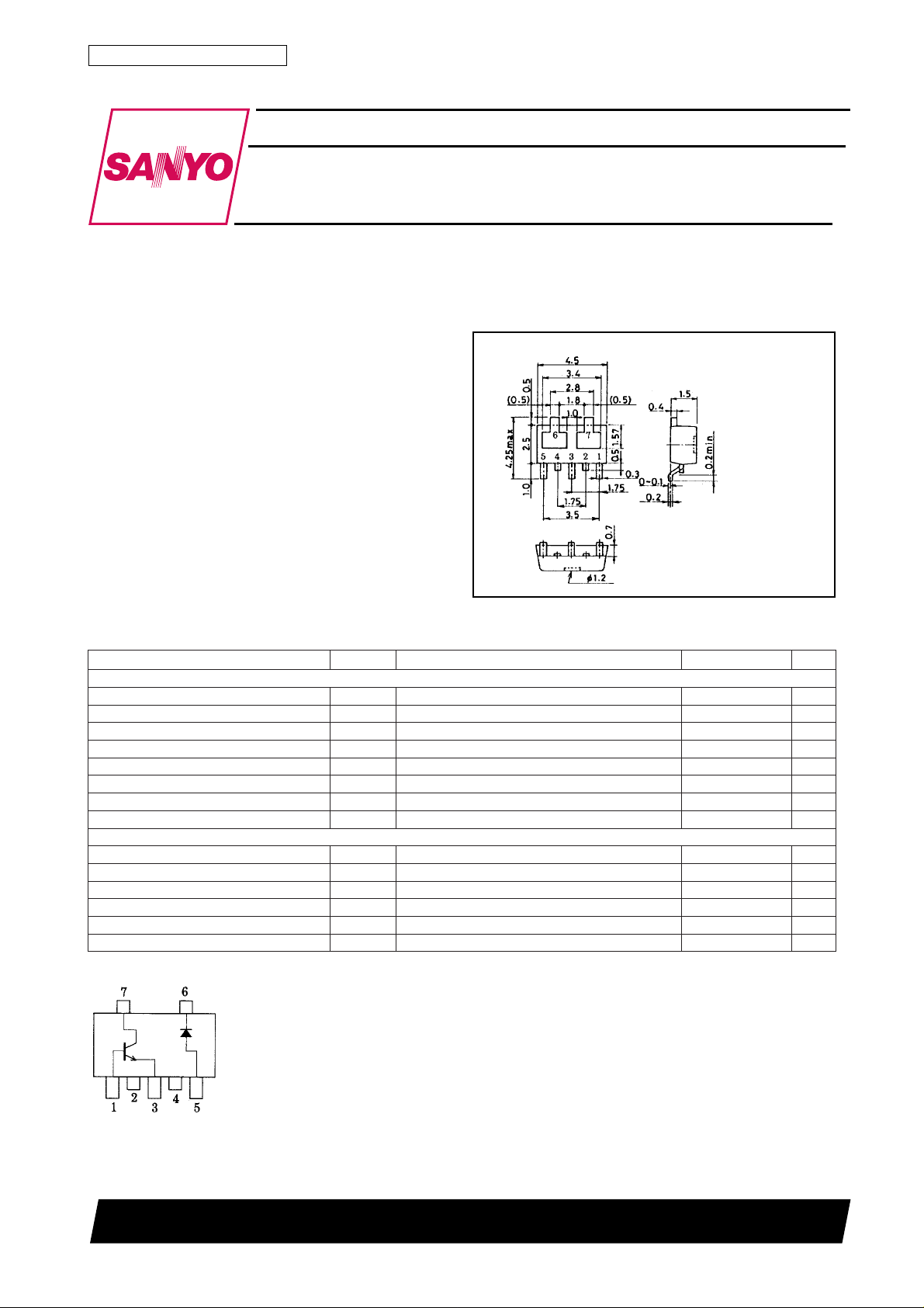
Package Dimensions
unit:mm
2099A
[FP301]
1:Base
2, 7:Collector
3:Emitter Common
4, 6:Collector
5:Base
SANYO:PCP5
(Bottom view)
2
×0.8mm)
elcyc1,evaweniszH05 5A
03V
52V
6V
2A
5A
004Am
8.0W
˚C
03V
53V
007Am
˚C
˚C
Electrical Connection
1:Base
2, 7:Collector
3:Emitter Common
4, 6:Collector
5:Base
(Top view)
52098HA (KT)/53094TH (KOTO) BX-0215 No.4539-1/4
Continued on next page.
Page 2
FP301
Continued from preceding page.
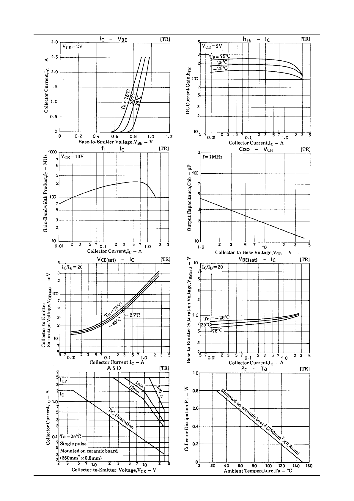
Electrical Characteristics at Ta=25˚C
retemaraPlobmySsnotidnoC
]RT[
tnerruCffotuCrotcelloCI
tnerruCffotuCrettimEI
niaGtnerruCCD
tcudorPhtdiwdnaB-niaGf
ecnaticapaCtuptuOboCV
egatloVnoitarutaSE-CV
egatloVnoitarutaSE-BV
egatloVnwodkaerBB-CV
egatloVnwodkaerBE-CV
egatloVnwodkaerBB-EV
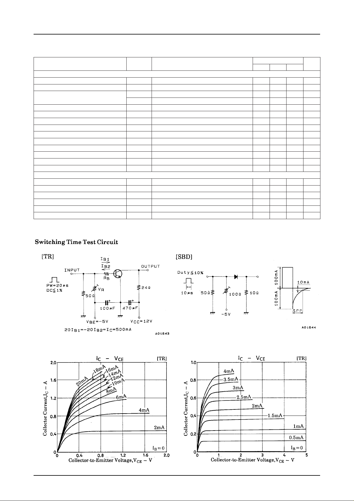
emiTNO-nruTt
emiTegarotSt
emiTllaFt
]DBS[
egatloVesreveRV
egatloVdrawroFV
tnerruCesreveRI
ecnaticapaClanimretretnICV
emiTyrevoceResreveRt
ecnatsiseRlamrehTa-jhtR 071
hEF1VECI,V2=
hEF2VECI,V2=
V
OBC
V
OBE
V
T
I
)tas(EC
C
I
)tas(EB
C
I
OBC)RB(
C
I
OEC)RB(
C
I
OBE)RB(
E
no
gts
f
I
R
R
I
F
F
VRV51= 08Aµ
R
R
IFI=
rr
Mounted on ceramic board (250mm2×0.8mm)
I,V02=
BC
BE
EC
EC
R
0=1.0Aµ
E
I,V4=
0=1.0Aµ
C
Am001=041065
C
A5.1=56
C
I,V01=
Am05=
C
zHM1=f,V01=
I,A5.1=
Am57=
B
I,A5.1=
Am57=58.02.1V
B
I,Aµ01=
0=03V
E
R,Am1=
=∞ 52V
EB
I,Aµ01=
0=6V
C
Aµ003=03V
Am007= 55.0V
tiucriCtseTdeificepseeS06sn
tiucriCtseTdeificepseeS005sn
tiucriCtseTdeificepseeS52sn
elcyczHM1=f,V01=82Fp
sgnitaR
nimpytxam
051zHM
91Fp
81.04.0V
.tiucriCtseTdeificpeseeS,Am001= 01sn
˚C/W
tinU
Marking:301
No.4539-2/4
Page 3
FP301
No.4539-3/4
Page 4

FP301
No products described or contained herein are intended for use in surgical implants, life-support systems,
aerospace equipment, nuclear power control systems, vehicles, disaster/crime-prevention equipment and
the like, the failure of which may directly or indirectly cause injury, death or property loss.
Anyone purchasing any products described or contained herein for an above-mentioned use shall:
Accept full responsibility and indemnify and defend SANYO ELECTRIC CO., LTD., its affiliates,
subsidiaries and distributors and all their officers and employees, jointly and severally, against any
and all claims and litigation and all damages, cost and expenses associated with such use:
Not impose any responsibilty for any fault or negligence which may be cited in any such claim or
litigation on SANYO ELECTRIC CO., LTD., its affiliates, subsidiaries and distributors or any of
their officers and employees jointly or severally.
Information (including circuit diagrams and circuit parameters) herein is for example only; it is not guarant-
eed for volume production. SANYO believes information herein is accurate and reliable, but no guarantees
are made or implied regarding its use or any infringements of intellectual property rights or other rights of
third parties.
This catalog provides information as of May, 1998. Specifications and information herein are subject to
change without notice.
PS No.4539-4/4
 Loading...