

Page 1
©2002 Fairchild Semiconductor Corporation
1
www.fairchildsemi.com
October 2002
FM809/810 3-Pin µC Supervisor Circuits
FM809/810 Rev. F
FM809/810
3-Pin µC Supervisor Circuits
General Description
The FM809/810 are supervisor circuits that monitor power
supply or other system voltages and issue reset pulse whenever
the voltage being monitored is out of tolerance. Once asserted,
the reset pulse is guaranteed to be valid for a minimum of
140ms (256ms typical). FM809xx offers active low push-pull
type of reset while FM810xx offers active high push-pull type.
Several threshold voltages are offered to accommodate 5.0V,
3.3V, 3.0V and 2.7V system voltages.
The low supply current (typically 2 µA)recommends FM809/810
devices for portable designs or wherever power saving is
primary.
These devices are offered in space saving 3-pin SOT23 and
SC70 packages.
Features
■
V
TH
voltages of 4.63V, 4.38V, 4.00V, 3.08V, 2.93V and 2.63V
■
RESET
(FM809) or RESET (FM810) output
■
140ms power-on RESET delay (minimum)
■
RESET operation guaranteed to 1.0V
■
Supply current only 2µA
■
No external components
■
Operating Range
– -40°C to +105°C (SOT23)
– -40°C to +85°C (SC70)
■
SOT23-3 and SC70-3 packages
Applications
■
Microcontrollers and Microprocessors
■
Appliances
■
Power-Supply Monitoring
■
Portable Equipment
■
Automotive Systems
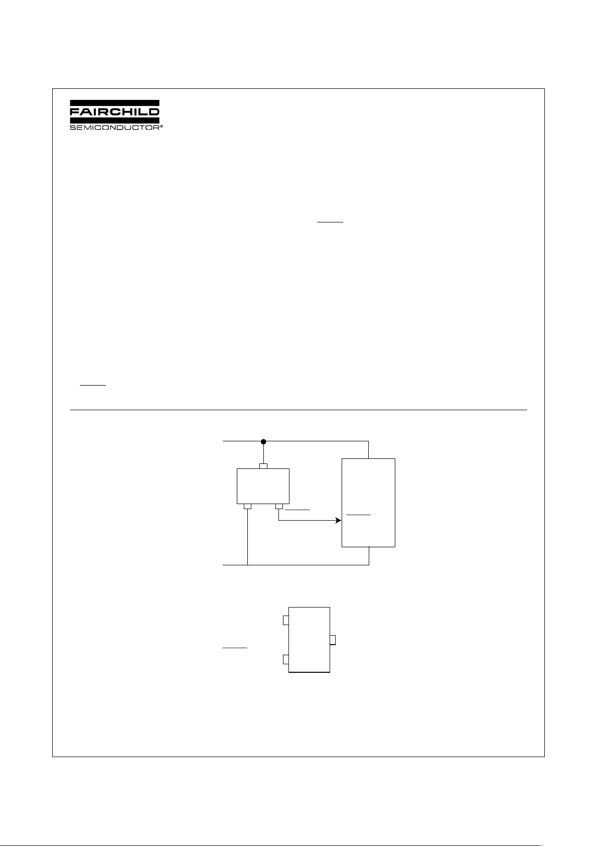
Typical Operating Circuit
Connection Diagram
FM809
µC
GND
V
CC
V
CC
GND
RESET
I/P
RESET
V
CC
3
GND
RESET (809) or
RESET (810)
1
2
FM809/810
SOT23-3 & SC70-3Packages
Page 2
FM809/810 3-Pin µC Supervisor Circuits
2
www.fairchildsemi.com
FM809/810 Rev. F
Absolute Maximum Ratings
Voltage on any terminal relative to GND
V
CC
-0.3V to +6.0V
RESET, RESET
-0.3V to (V
CC
+ 0.3V)
Input Current 20mA
Output Current: RESET, RESET
20mA
ESD Rating
Human Body Model >2KV
Machine Model >200KV
Rate of Rise of V
CC
100V/µs
Continuous Power Dissipation (T
A
= +70°C)
SOT23-3 (derate 4mW/°C above +70°C) 320mW
Operating Temperature Range -40°C to +105°C
Storage Temperature Range -65°C to +150°C
Lead Temperature (soldering, 10s) +300°C
These are stress ratings only, and functional operation is not implied for these levels or beyond. Exposure to Absolute Maximum
Rating conditions for extended periods may affect device reliability.
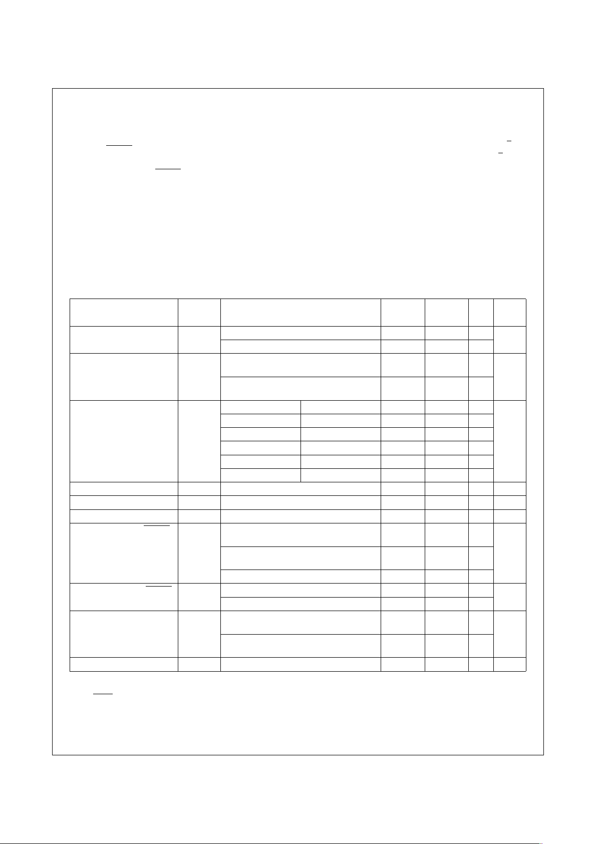
Electrical Characteristics
SOT23 Package (T
A
= 25°C unless otherwise noted)
V
CC
= full range, as noted under conditions. See Note 1.
Note 1: Testing in production is 25°C only. V
CC
= 5V for FM8xxL/M/J, V
CC
= 3.3V for FM8xxT/S and V
CC
= 3V for FM8xxR. Limits over temperature are guaranteed by design.
Note 2 : RESET
output is for FM809. RESET output is for FM810.
Note 3 : Typical values are at 25°C.
Note 4: Recommended minimum slew rate for the V
CC
rampup is 200mV/sec in the 0 to 2V range for the device to function properly.
Parameter Symbol Conditions Min
Typ
(Note 3) Max Units
Operating Voltage V
CC
T
A
= 0°C to +70°C 1.0 5.5 V
T
A
= -40°C to 105°C 1.1 5.5
Supply Current I
CC
T
A
= -40°C to 105°C, V
CC
< 5.5V
FM809J/L/M
510µA
T
A
= -40°C to 105°C, V
CC
< 3.6V
FM809R/S/T
26
Reset Threshold V
TH
FM8xxL T
A
= -40°C to +105°C 4.40 4.63 4.86 V
FM8xxM T
A
= -40°C to +105°C 4.18 4.38 4.52
FM8xxJ T
A
= -40°C to +105°C 3.90 4.00 4.18
FM8xxT T
A
= -40°C to +105°C 2.97 3.08 3.19
FM8xxS T
A
= -40°C to +105°C 2.79 2.93 3.00
FM8xxR T
A
= -40°C to +105°C 2.49 2.63 2.70
Reset Threshold Tempco 30 ppm/°C
V
CC
to Reset Delay (Note 2) V
CC
= V
TH
to (V
TH
- 100mV) 10 15 µs
Reset Active Timout Period T
A
= -40°C to +105°C 140 256 560 ms
FM809 Output Low (RESET)V
OL
V
CC
= V
TH
(min), I
SINK
= 1.2mA,
FM809R/S/T
0.3 V
V
CC
= V
TH
(min), I
SINK
= 3.2mA,
FM809J/L/M
0.4
V
CC
= < 1.0V, I
SINK
= 50µA 0.3
FM809 Output High (RESET)V
OH
V
CC
> V
TH
(max), I
SOURCE
= 500µA (R/S/T) 0.8V
CC
V
V
CC
> V
TH
(max), I
SOURCE
= 800µA (J/M/L) V
CC
- 1.5V
FM810 Output Low (RESET) V
OL
V
CC
= V
TH
(max), I
SINK
= 1.2mA,
FM810R/S/T
0.3 V
V
CC
= V
TH
(max), I
SINK
= 3.2mA,
FM810J/L/M
0.4
FM810 Output High (RESET) V
OH
1.8V < V
CC
< V
TH
(min), I
SOURCE
= 150µA 0.8V
CC
V
Page 3
FM809/810 3-Pin µC Supervisor Circuits
3
www.fairchildsemi.com
FM809/810 Rev. F
Absolute Maximum Ratings
Voltage on any terminal relative to GND
V
CC
-0.3V to +6.0V
RESET, RESET
-0.3V to (V
CC
+ 0.3V)
Input Current 20mA
Output Current: RESET, RESET
20mA
ESD Rating
Human Body model 1.5KV
Machine model >200KV
Rate of Rise of V
CC
100V/µs
Continuous Power Dissipation (T
A
= +70°C)
SC70-3 174mW
Operating Temperature Range -40°C to +85°C
Storage Temperature Range -65°C to +150°C
Lead Temperature (soldering, 10s) +300°C
These are stress ratings only, and functional operation is not implied for these levels or beyond. Exposure to Absolute Maximum
Rating conditions for extended periods may affect device reliability.
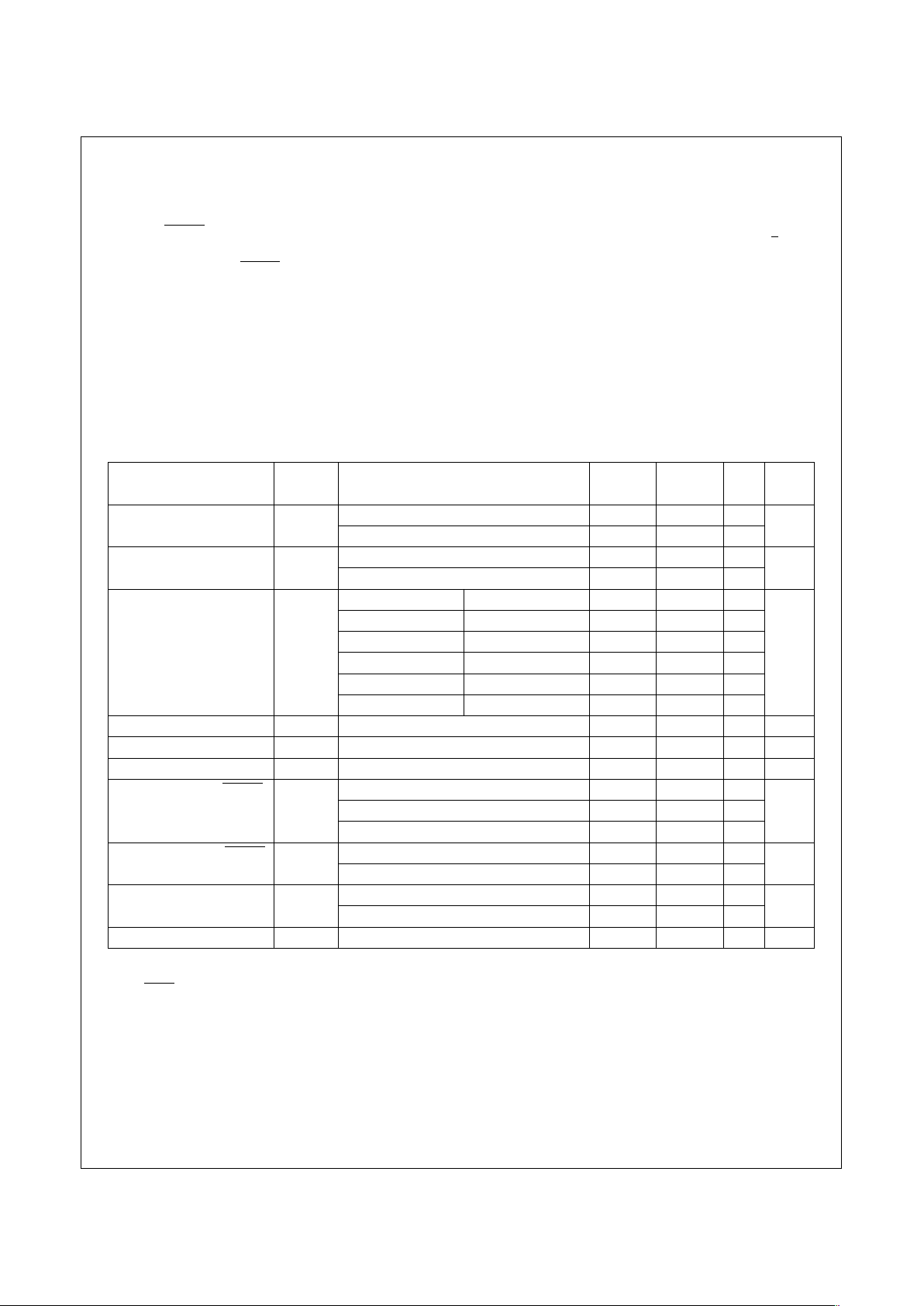
Electrical Characteristics
SC70 Package (T
A
= 25°C unless otherwise noted)
V
CC
= full range, as noted under conditions. See Note 1.
Note 1: Testing in production is 25°C only. V
CC
= 5V for FM8xxL/M/J, V
CC
= 3.3V for FM8xxT/S and V
CC
= 3V for FM8xxR. Limits over temperature are guaranteed by design.
Note 2: RESET
output is for FM809. RESET output is for FM810.
Note 3: Typical values are at 25°C.
Parameter Symbol Conditions Min
Typ
(Note 3) Max Units
Operating Voltage V
CC
T
A
= 0°C to +70°C 1.4 5.5 V
T
A
= -40°C to 85°C 1.6 5.5
Supply Current I
CC
T
A
= -40°C to 85°C, V
CC
< 5.5V FM809J/L/M 9 15 µA
T
A
= -40°C to 85°C, V
CC
< 3.6V FM809R/S/T 6 10
Reset Threshold V
TH
FM8xxL T
A
= -40°C to +85°C 4.40 4.63 4.86 V
FM8xxM T
A
= -40°C to +85°C 4.18 4.38 4.52
FM8xxJ T
A
= -40°C to +85°C 3.90 4.00 4.18
FM8xxT T
A
= -40°C to +85°C 2.97 3.08 3.19
FM8xxS T
A
= -40°C to +85°C 2.79 2.93 3.00
FM8xxR T
A
= -40°C to +85°C 2.49 2.63 2.70
Reset Threshold Tempco 30 ppm/°C
V
CC
to Reset Delay (Note 2) V
CC
= V
TH
to (V
TH
- 100mV) 10 15 µs
Reset Active Timout Period T
A
= -40°C to +85°C 100 256 560 ms
FM809 Output Low (RESET)V
OL
V
CC
= V
TH
(min), I
SINK
= 1.2mA, FM809R/S/T 0.35 V
V
CC
= V
TH
(min), I
SINK
= 3.2mA, FM809J/L/M 0.4
V
CC
= < 1.0V, I
SINK
= 50µA 0.3
FM809 Output High (RESET)V
OH
V
CC
> V
TH
(max), I
SOURCE
= 500µA (R/S/T) 0.8V
CC
V
VCC > VTH(max), I
SOURCE
= 800µA (J/M/L) VCC - 1.5V
FM810 Output Low (RESET) V
OL
VCC = VTH(max), I
SINK
= 1.2mA, FM810R/S/T 0.35 V
VCC = VTH(max), I
SINK
= 3.2mA, FM810J/L/M 0.4
FM810 Output High (RESET) V
OH
1.8V < VCC < VTH(min), I
SOURCE
= 150µA 0.8V
CC
V
Page 4

FM809/810 3-Pin µC Supervisor Circuits
4 www.fairchildsemi.com
FM809/810 Rev. F
Pin Descriptions
* with overbar, FM809 (RESET); without, FM810 (RESET).
Circuit Timing (e.g.: FM809)
When operating properly with 5V in (for example), V
OUT
will also
be about 5V. When VIN starts to fall, V
OUT
will follow it down as
shown. When VIN drops below VTH, V
OUT
drops to ground
("issues a RESET") and stays there unless VIN also falls below
its minimum operating voltage, approx. 1V. At this point, the
supervisor loses control, and its output may rise, only to again
follow VIN down to the ground.
When VIN begins to rise, V
OUT
follows it until 1.0V or so is
reached, whereupon the device regains control, V
OUT
is pulled
to ground, etc. When VIN rises above VTH, V
OUT
comes out of
RESET 140 ms later.
If it is required that a lower value than GND + 1.0V is needed
on RESET signal during VCC ≤ 1V, a 100K resistor may be used
on the device output (to GND for the FM809, to VCC for the
FM810).
Pin Number Name Function
1 GND GROUND
2 RESET* RESET (RESET) remains LOW (HIGH) while VCC is below VTH,
and for at least 140ms after VCC rises above VTH.
3V
CC
5V
V
TH
1V
GND
5V
V
TH
1V
GND
INPUT
OUTPUT
140ms
Page 5

FM809/810 3-Pin µC Supervisor Circuits
5 www.fairchildsemi.com
FM809/810 Rev. F
Ordering Information (FM809)
Note 4: Devices listed above feature 250ms typical Reset Pulse width. Consult Fairchild sales for other reset pulse width options.
Part Number Top Marking
RESET
Threshold (V) Output Type Package Type
Packing
Method
FM809LS3X 09L 4.63 Push-Pull, active LOW 3-Pin, SOT23 3000 units in T&R
FM809MS3X 09M 4.38 Push-Pull, active LOW 3-Pin, SOT23 3000 units in T&R
FM809JS3X 09J 4.00 Push-Pull, active LOW 3-Pin, SOT23 3000 units in T&R
FM809TS3X 09T 3.08 Push-Pull, active LOW 3-Pin, SOT23 3000 units in T&R
FM809SS3X 09S 2.93 Push-Pull, active LOW 3-Pin, SOT23 3000 units in T&R
FM809RS3X 09R 2.63 Push-Pull, active LOW 3-Pin, SOT23 3000 units in T&R
FM809LP3X VLY 4.63 Push-Pull, active LOW 3-Pin, SC70 3000 units in T&R
FM809MP3X VMY 4.38 Push-Pull, active LOW 3-Pin, SC70 3000 units in T&R
FM809JP3X VJY 4.00 Push-Pull, active LOW 3-Pin, SC70 3000 units in T&R
FM809TP3X VTY 3.08 Push-Pull, active LOW 3-Pin, SC70 3000 units in T&R
FM809SP3X VSY 2.93 Push-Pull, active LOW 3-Pin, SC70 3000 units in T&R
FM809RP3X VRY 2.63 Push-Pull, active LOW 3-Pin, SC70 3000 units in T&R
Page 6

FM809/810 3-Pin µC Supervisor Circuits
6 www.fairchildsemi.com
FM809/810 Rev. F
Ordering Information (FM810)
Note 5: Devices listed above feature 250ms typical Reset Pulse width. Consult Fairchild sales for other reset pulse width options.
Part Number Top Marking
RESET
Threshold (V) Output Type Package Type
Packing
Method
FM810LS3X 10L 4.63 Push-Pull, active HIGH 3-Pin, SOT23 3000 units in T&R
FM810MS3X 10M 4.38 Push-Pull, active HIGH 3-Pin, SOT23 3000 units in T&R
FM810JS3X 10J 4.00 Push-Pull, active HIGH 3-Pin, SOT23 3000 units in T&R
FM810TS3X 10T 3.08 Push-Pull, active HIGH 3-Pin, SOT23 3000 units in T&R
FM810SS3X 10S 2.93 Push-Pull, active HIGH 3-Pin, SOT23 3000 units in T&R
FM810RS3X 10R 2.63 Push-Pull, active HIGH 3-Pin, SOT23 3000 units in T&R
FM810LP3X ZLY 4.63 Push-Pull, active HIGH 3-Pin, SC70 3000 units in T&R
FM810MP3X ZMY 4.38 Push-Pull, active HIGH 3-Pin, SC70 3000 units in T&R
FM810JP3X ZJY 4.00 Push-Pull, active HIGH 3-Pin, SC70 3000 units in T&R
FM810TP3X ZTY 3.08 Push-Pull, active HIGH 3-Pin, SC70 3000 units in T&R
FM810SP3X ZSY 2.93 Push-Pull, active HIGH 3-Pin, SC70 3000 units in T&R
FM810RP3X ZRY 2.63 Push-Pull, active HIGH 3-Pin, SC70 3000 units in T&R
Page 7

7 www.fairchildsemi.com
FM809/810 Rev. F
FM809/810 3-Pin µC Supervisor Circuits
Physical Dimensions inches (millimeters) unless otherwise noted
0
.12
0
0.105
0.079
0.071
0.004
0.001
0.040
0.031
0.021
0.015
0.055
0.047
0.098
0.083
0.010
0.005
0.0059
0.0035
0-8
PK
G
C
L
0.76
0.76
0.95
2.29
LAND PATTERN RECOMMENDATION
SOT-23 Package Dimensions
FS Pkg Code AU
Page 8

8 www.fairchildsemi.com
FM809/810 Rev. F
FM809/810 3-Pin µC Supervisor Circuits
Life Support Policy
Fairchild's products are not authorized for use as critical components in life support devices or systems without the express written
approval of the President of Fairchild Semiconductor Corporation. As used herein:
1. Life support devices or systems are devices or systems which,
(a) are intended for surgical implant into the body, or (b) support
or sustain life, and whose failure to perform, when properly
used in accordance with instructions for use provided in the
labeling, can be reasonably expected to result in a significant
injury to the user.
2. A critical component is any component of a life support
device or system whose failure to perform can be reasonably
expected to cause the failure of the life support device or
system, or to affect its safety or effectiveness.
Fairchild Semiconductor Fairchild Semiconductor Fairchild Semiconductor Fairchild Semiconductor
Americas Europe Hong Kong Japan Ltd.
Customer Response Center Fax: +44 (0) 1793-856858 8/F, Room 808, Empire Centre 4F, Natsume Bldg.
Tel. 1-888-522-5372 Deutsch Tel: +49 (0) 8141-6102-0 68 Mody Road, Tsimshatsui East 2-18-6, Yushima, Bunkyo-ku
English Tel: +44 (0) 1793-856856 Kowloon. Hong Kong Tokyo, 113-0034 Japan
Fran çais Tel: +33 (0) 1-6930-3696 Tel; +852-2722-8338 Tel: 81-3-3818-8840
Italiano Tel: +39 (0) 2-249111-1 Fax: +852-2722-8383 Fax: 81-3-3818-8841
Physical Dimensions inches (millimeters) unless otherwise noted
.004 (.10)
.026
(.65)
.052
(1.3)
.087 (2.2)
.071 (1.8)
.016 (.40)
.012 (.30)
.043 (1.1)
.032 (.80)
.018 (.45)
.006 (.15)
.010 (.25)
.004 (.10)
.009 (.23)
.005 (.13)
.087 (2.2)
.079 (2.0)
.053 (1.35)
.045 (1.15)
Land Pattern Recommendation
0.65
1.80
0.5
0.6
0.65
SC70 Package Dimensions
 Loading...