

Page 1
tm
FDP52N20 / FDPF52N20T N-Channel MOSFET
FDP52N20 / FDPF52N20T
N-Channel MOSFET
200V, 52A, 0.049Ω
Features
•R
• Low gate charge ( Typ. 49nC)
• Low C
• Fast switching
• 100% avalanche tested
• Improve dv/dt capability
• RoHS compliant
= 0.041Ω ( Typ.)@ VGS = 10V, ID = 26A
DS(on)
( Typ. 66pF)
rss
Description
These N-Channel enhancement mode power field effect transistors are produced using Fairchild’s proprietary, planar stripe,
DMOS technology.
This advance technology has been especially tailored to minimize on-state resistance, provide superior switching performance, and withstand high energy pulse in the avalanche and
commutation mode. These devices are well suited for high efficient switching mode power supplies and active power factor
correction.
October 2007
TM
UniFET
D
G
G
S
D
MOSFET Maximum Ratings T
Symbol Parameter FDP52N20 FDPF52N20T Units
V
DSS
V
GSS
I
D
I
DM
E
AS
I
AR
E
AR
dv/dt Peak Diode Recovery dv/dt (Note 3) 4.5 V/ns
P
D
, T
T
J
STG
T
L
*Drain current limited by maximum junction temperature
Drain to Source Voltage 200 V
Gate to Source Voltage ±30 V
D r a i n C urrent
Drain Current - Pulsed (Note 1) 208 208* A
Single Pulsed Avalanche Energy (Note 2) 2520 mJ
Avalanche Current (Note 1) 52 A
Repetitive Avalanche Energy (Note 1) 35.7 mJ
Power Dissipation
Operating and Storage Temperature Range -55 to +150
Maximum Lead Temperature for Soldering Purpose,
1/8” from Case for 5 Seconds
TO-220
FDP Series
D
G
S
= 25oC unless otherwise noted
C
-Continuous (T
-Continuous (T
(T
= 25oC) 357 38.5 W
C
- Derate above 25
TO-220F
FDPF Series
= 25oC) 52 52*
C
= 100oC) 33 33*
C
o
C 2.86 0.3 W/oC
S
300
o
o
Thermal Characteristics
Symbol Parameter FDP52N20 FDPF52N20T Units
R
θJC
θCS
R
θJA
Thermal Resistance, Junction to Case 0.35 3.3
Thermal Resistance, Case to Sink Typ. 0.5 Thermal Resistance, Junction to Ambient 62.5 62.5
o
C/WR
A
C
C
©2007 Fairchild Semiconductor Corporation
FDP52N20 / FDPF52N20T Rev. A
www.fairchildsemi.com1
Page 2
FDP52N20 / FDPF52N20T N-Channel MOSFET
Package Marking and Ordering Information T
= 25oC unless otherwise noted
C
Device Marking Device Package Reel Size Tape Width Quantity
FDP52N20 FDP52N20 TO-220 - - 50
FDPF52N20T FDPF52N20T TO-220F - - 50
Electrical Characteristics
Symbol Parameter Test Conditions Min. Typ. Max. Units
Off Characteristics
BV
DSS
∆BV
DSS
/ ∆T
J
I
DSS
I
GSS
On Characteristics
V
GS(th)
R
DS(on)
g
FS
Dynamic Characteristics
C
iss
C
oss
C
rss
Q
g(tot)
Q
gs
Q
gd
Drain to Source Breakdown Voltage ID = 250µA, VGS = 0V, TJ = 25oC 200 - - V
Breakdown Voltage Temperature
Coefficient
Zero Gate Voltage Drain Current
Gate to Body Leakage Current VGS = ±30V, V
I
= 250µA, Referenced to 25oC-0.2-V/
D
V
= 200V, V
DS
= 160V, TC = 125oC--10
V
DS
= 0V - - 1
GS
= 0V - - ±100 nA
DS
Gate Threshold Voltage VGS = VDS, ID = 250µA3.0-5.0V
Static Drain to Source On Resistance VGS = 10V, ID = 26A - 0.041 0.049 Ω
Forward Transconductance VDS = 40V , ID = 26A (Note 4) -35-S
Input Capacitance
Output Capacitance - 540 700 pF
Reverse Transfer Capacitance - 66 100 pF
= 25V, VGS = 0V
V
DS
f = 1MHz
Total Gate Charge at 10V
V
= 160V, ID = 52A
Gate to Source Gate Charge - 19 - nC
Gate to Drain “Miller” Charge - 24 - nC
DS
V
= 10V
GS
(Note 4, 5)
- 2230 2900 pF
-4963nC
µA
o
C
Switching Characteristics
t
d(on)
t
r
t
d(off)
t
f
Turn-On Delay Time
Turn-On Rise Time - 175 359 ns
Turn-Off Delay Time - 48 107 ns
Turn-Off Fall Time - 29 68 ns
Drain-Source Diode Characteristics
I
S
I
SM
V
SD
t
rr
Q
rr
Notes:
1. Repetitive Rating: Pulse width limited by maximum junction temperature
2. L = 1.4mH, IAS = 52A, VDD = 50V, RG = 25Ω, Starting TJ = 25°C
3. ISD ≤ 52A, di/dt ≤ 200A/µs, VDD ≤ BV
4. Pulse Test: Pulse width ≤ 300µs, Duty Cycle ≤ 2%
5. Essentially Independent of Operating Temperature Typical Characteristics
Maximum Continuous Drain to Source Diode Forward Current - - 52 A
Maximum Pulsed Drain to Source Diode Forward Current - - 204 A
Drain to Source Diode Forward Voltage V
Reverse Recovery Time
Reverse Recovery Charge - 1.3 - µC
, Starting TJ = 25°C
DSS
= 100V, ID = 20A
V
DD
R
= 25Ω
G
(Note 4, 5)
= 0V, I
GS
V
= 0V, I
GS
dI
/dt = 100A/µs (Note 4)
F
= 52A - - 1.5 V
SD
= 52A
SD
- 53 115 ns
- 162 - ns
FDP52N20 / FDPF52N20T Rev. A
2
www.fairchildsemi.com
Page 3
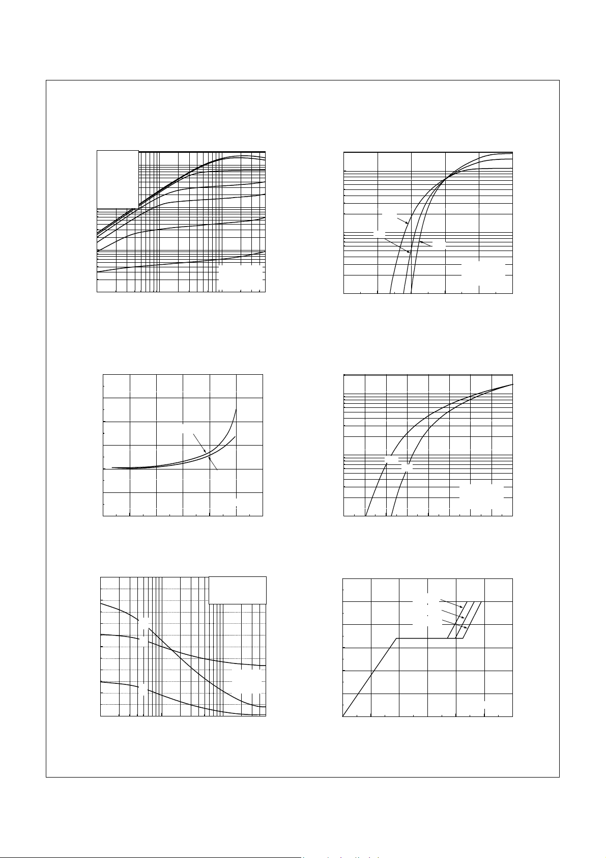
Typical Performance Characteristics
FDP52N20 / FDPF52N20T N-Channel MOSFET
Figure 1. On-Region Characteristics Figure 2. Transfer Characteristics
V
GS
Top : 1 5 .0 V
2
10
10.0 V
8.0 V
7.0 V
6.5 V
6.0 V
Bo ttom : 5.5 V
1
10
0
10
, Drain Current [A]
D
I
-1
10
-1
10
VDS, Drain-Source Voltage [V]
2
10
150°C
1
10
25°C
-55°C
, Drain Current [A]
D
I
* Note s :
µs P ulse Test
1. 250
= 25°C
2. T
C
0
10
1
10
0
10
24681012
* Note s :
1. V
2. 25 0
= 40V
DS
µs Pulse Test
VGS, G a te -Sou r c e V o lta g e [V]
Figure 3. On-Resistance Variation vs. Figure 4. Body Diode Forward Voltage
Drain Current and Gate Voltage Variation vs. Source Current
and Temperature
0.12
0.10
0.08
[Ω],
0.06
DS(ON)
R
0.04
0.02
Drain-Source On-Resistance
0.00
0 25 50 75 100 125 150
VGS = 10V
ID, Drain Current [A]
VGS = 20V
* No te : TJ = 25°C
2
10
1
10
150℃
25℃
, Reverse Drain Current [A]
DR
I
0
10
0.2 0.4 0.6 0.8 1.0 1.2 1.4 1.6 1.8
* Notes :
1. V
2. 25 0
= 0V
GS
µs Pulse Test
VSD, S o u rc e-D rain v oltag e [V]
Figure 5. Capacitance Characteristics Figure 6. Gate Charge Characteristics
6000
5000
4000
3000
2000
Capacitances [pF]
1000
0
-1
10
FDP52N20 / FDPF52N20T Rev. A
C
oss
C
iss
C
rss
VDS, Drain-Source Voltage [V]
C
= Cgs + Cgd (Cds = shorted)
iss
C
= Cds + C
oss
gd
C
= C
rss
gd
12
10
VDS = 40V
VDS = 100V
8
* No te ;
= 0 V
1. V
GS
2. f = 1 MHz
0
10
1
10
6
4
, Gate-Source Voltage [V]
2
GS
V
0
0 102030405060
VDS = 160V
* No te : ID = 52A
QG, To ta l Gate Charg e [n C]
3
www.fairchildsemi.com
Page 4

Typical Performance Characteristics (Continued)
Figure 7. Breakdown Voltage Variation Figure 8. On-Resistance Variation
vs. Temperature vs. Temperature
1.2
3.0
2.5
1.1
2.0
FDP52N20 / FDPF52N20T N-Channel MOSFET
1.0
, (Normalized)
DSS
BV
0.9
* No tes :
1. V
2. I
Drain-Source Breakdown Voltage
0.8
-100 -50 0 50 100 150 200
TJ, Junction Temperature [°C]
= 0 V
GS
= 250µA
D
1.5
, (Normalized)
1.0
DS(ON)
R
0.5
Drain-Source On-Resi stance
0.0
-100 -50 0 50 100 150 200
TJ, Junction Temperature [°C]
* Notes :
1. V
2. I
GS
= 26 A
D
= 10 V
Figure 9-1. Maximum Safe Operating Area Figure 9-2. Maximum Safe Operating Area
- FDP52N20 - FDPF52N20T
3
10
2
10
1
10
Operation in This Area
0
10
, Drain Current [A]
D
I
-1
10
-2
10
10
is Limited by R
0
10 ms
100 ms
DC
DS(on)
* No tes :
1. T
2. T
3. S ing le Pulse
1
10
VDS, Drain-Source Voltage [V]
1 ms
= 25°C
C
= 150°C
J
10
100 µs
2
10 µs
3
10
2
10
10 µs
100 µs
DC
10 ms
100 ms
1 ms
* No tes :
= 25°C
1. T
C
= 150°C
2. T
J
3. S ing le Pulse
2
10
1
10
10
, Drain Current [A]
D
I
-1
10
-2
10
Operation in This Area
is Limited by R
0
0
10
DS(on)
1
10
VDS, Drain-Source Voltage [V]
Figure 10. Maximum Drain Current
60
50
40
30
20
, Drain Current [A]
D
I
10
0
25 50 75 100 125 150
TC, Case Temperature [°C]
FDP52N20 / FDPF52N20T Rev. A
4
www.fairchildsemi.com
Page 5

Typical Performance Characteristics (Continued)
Figure 11-1. Transient Thermal Response Curve - FDP52N20
D=0.5
-1
10
0.2
-2
10
(t), Thermal Response
θJC
Z
0.1
0.05
0.02
0.01
single pulse
P
DM
t
1
t
* Notes :
1. Z
2. D u ty Fac to r , D=t
3. TJM - TC = PDM * Z
2
(t) = 0.35 0C/W Max.
θJC
1/t2
(t)
θJC
FDP52N20 / FDPF52N20T N-Channel MOSFET
-5
10
-4
10
-3
10
-2
10
-1
10
0
10
1
10
t1, Sq ua re Wave P ulse D u ratio n [s ec ]
Figure 11-2. Transient Thermal Response Curve - FDPF52N20T
D=0.5
0
10
0.2
0.1
P
DM
t
1
t
* Notes :
1. Z
2. Du ty Facto r , D=t
3. TJM - TC = PDM * Z
10
2
(t) = 3.3 0C/W Max.
θJC
-1
10
1/t2
(t)
θJC
0
1
10
-1
10
(t), Thermal Response
θJC
Z
-2
10
-5
10
0.05
0.02
0.01
sing le puls e
-4
10
-3
10
-2
10
t1, Square W ave P ulse Duration [sec]
FDP52N20 / FDPF52N20T Rev. A
5
www.fairchildsemi.com
Page 6

Gate Charge Test Circuit & Waveform
Resistive Switching Test Circuit & Waveforms
FDP52N20 / FDPF52N20T N-Channel MOSFET
FDP52N20 / FDPF52N20T Rev. A
Unclamped Inductive Switching Test Circuit & Waveforms
6
www.fairchildsemi.com
Page 7

Peak Diode Recovery dv/dt Test Circuit & Waveforms
g
g
+
+
V
V
DS
DS
_
_
L
LL
Sam e Type
Sam e Type
as DUT
as DUT
• dv/dt controlled by R
• dv/dt controlled by R
•ISDcontrolled by pulse period
•ISDcontrolled by pulse period
G
G
V
V
GS
GS
R
R
Driver
Driver
G
G
DUT
DUT
I
I
SD
SD
V
V
DD
DD
FDP52N20 / FDPF52N20T N-Channel MOSFET
V
V
GS
GS
( D riv er )
( D riv er )
I
I
SD
SD
( DUT )
( DUT )
V
V
DS
DS
( DUT )
( DUT )
G ate P ulse W idth
G ate P ulse W idth
G ate P ulse W idth
--------------------------
--------------------------
--------------------------
D =
D =
D =
Gate Pulse Period
Gate Pulse Period
Gate Pulse Period
IFM, Body Diode Forward C urrent
IFM, Body Diode Forward C urrent
I
I
RM
RM
Body Diode Reverse Current
Body Diode Reverse Current
Body Diode R ecovery dv/dt
Body Diode R ecovery dv/dt
V
V
SD
SD
Body Diode
Body Diode
e Drop
Forward Volta
Forward Volta
e Drop
di/dt
di/dt
10V
10V
V
V
DD
DD
FDP52N20 / FDPF52N20T Rev. A
7
www.fairchildsemi.com
Page 8

Mechanical Dimensions
FDP52N20 / FDPF52N20T N-Channel MOSFET
TO - 220
FDP52N20 / FDPF52N20T Rev. A
Dimensions in Millimeters
8
www.fairchildsemi.com
Page 9

Mechanical Dimensions
0
0
10.16
±0.1
3.30
±0.20
(7.00)
TO-220F
ø3.18
±0.10
±0.20
6.68
2.54
(0.70)
FDP52N20 / FDPF52N20T N-Channel MOSFET
±0.20
±0.20
±0.20
(1.00x45°)
15.87
15.80
MAX1.47
±0.30
0.80
±0.10
9.75
(30°)
#1
0.35
2.54TYP
±0.20
[2.54
±0.10
2.54TYP
]
9.40
±0.20
[2.54
±0.20
±0.20
]
0.50
+0.10
–0.05
2.76
±0.2
4.70
FDP52N20 / FDPF52N20T Rev. A
Dimensions in Millimeters
9
www.fairchildsemi.com
Page 10

TRADEMARKS
The following are registered and unregistered trademarks and service marks Fairchild Semiconductor owns or is authorized to use and is not
intended to be an exhaustive list of all such trademarks.
®
ACEx
Build it Now™
CorePLUS™
CROSSVOLT™
CTL™
Current Transfer Logic™
EcoSPARK
Fairchild
®
®
®
Fairchild Semiconduct or
FACT Quiet Series™
®
FACT
®
FAST
FastvCore™
FPS™
®
FRFET
Global Power ResourceSM
Green FPS™
Green FPS™ e-Series™
GTO™
i-Lo™
IntelliMAX™
ISOPLANAR™
MegaBuck™
MICROCOUPLER™
MicroFET™
MicroPak™
®
MillerDrive™
Motion-SPM™
OPTOLOGIC
OPTOPLANAR
®
PDP-SPM™
Power220
®
®
®
Power247
POWEREDGE
Power-SPM™
PowerTrench
Programmable Active Droop™
QFET
QS™
QT Optoelectronics™
Quiet Series™
RapidConfigure™
SMART START™
SPM
STEALTH™
SuperFET™
SuperSOT™-3
SuperSOT™-6
DISCLAIMER
FAIRCHILD SEMICONDUCTOR RESERVES THE RIGHT TO MAKE CHANGES WITHOUT FURTHER NOTICE TO ANY PR ODUCTS
HEREIN TO IMPROVE RELIABILITY, FUNCTION, OR DESIGN. FAIRCHILD DOES NOT ASSUME ANY LIABILITY ARISING OUT OF THE
APPLICATION OR USE OF AN Y PRODUCT OR CIRCUIT DESCRIBED HEREIN; NEITHER DOES IT CONVEY ANY LICENSE UNDER ITS
PATENT RIGHTS, NOR THE RIG HTS OF OTH ERS. THESE SPECIFICATIO NS DO N OT EXPAN D THE TERM S OF FAIRCHILD’S
WORLDWIDE TERMS AND CONDITIONS, SPECIFIC ALLY THE WARRANTY THER EIN, WHICH COVERS TH ESE PRODUCTS.
LIFE SUPPORT POLICY
FAIRCHILD’S PRODUCTS ARE NOT AUTHORIZED FOR USE AS CRITICAL COMPONENTS IN LIFE SUPPORT DEVICES OR
SYSTEMS WITHOUT THE EXPRESS WRITTEN APPROVAL OF FAIRCHILD SEMICONDUCTOR CORPORATION.
As used herein:
1. Life support devices or systems are devices or systems
2. A critical component in any component of a life support,
which, (a) are intended for surgical im plant into the body or
(b) support or sustain lif e, and (c) whose failure to perform
when properly used in accordance with instructi ons for use
provided in the labeling, can be reasonably expected to
result in a signific ant injury of the user.
PRODUCT STATUS DEFINITIONS
Definition of Terms
Datasheet Identification Product Status Definition
Advance Information Formative or In Design This datasheet contains the design specifications for product
development. Specif i cations may change in any manner without notice.
Preliminary First Production This datasheet contains preliminary data; supplementary data will be
published at a later date. Fairc hi l d Semiconductor reserves the right to
make changes at any ti me without notice to improve design.
No Identification Needed Full Production This datasheet contains final specif i cations. Fairchild Semiconductor
reserves the right to make changes at any tim e without notice to improve
design.
Obsolete Not In Production This datasheet contai ns specifications on a product that has been
discontinued by Fairchild Semiconductor. The datasheet is printed for
reference information only.
®
®
®
®
SuperSOT™-8
SyncFET™
The Power Franchise
TinyBoost™
TinyBuck™
TinyLogic
®
®
TINYOPTO™
TinyPower™
®
TinyPWM™
TinyWire™
μSerDes™
®
UHC
UniFET™
VCX™
device, or system whose failure to perform can be
reasonably expected to cause the fail ure of the life support
device or system, or to affect its safety or effectiveness.
Rev. I31
© 2007 Fairchild Semiconductor Corporation www.fairchildsemi.com
 Loading...