

Page 1
tm
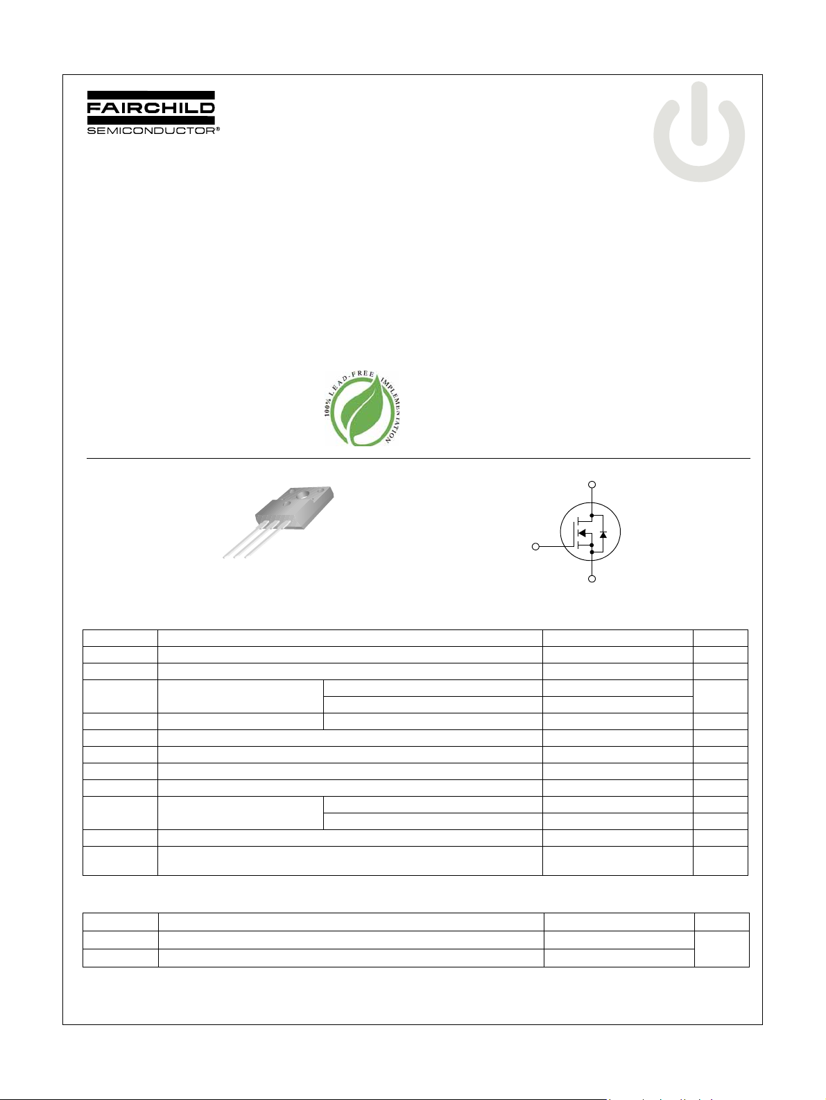
FDPF3860T
N-Channel PowerTrench® MOSFET
100V, 20A, 38.2mΩ
FDPF3860T N-Channel PowerTrench
March 2008
Description
•R
• Fast switching speed
• Low gate charge
• High performance trench technology for extremely low R
• High power and current handling capability
• RoHS compliant
MOSFET Maximum Ratings T
V
DSS
V
GSS
I
D
I
DM
E
AS
I
AR
E
AR
dv/dt Peak Diode Recovery dv/dt (Note 3) 15 V/ns
P
D
, T
T
J
T
L
= 38.2mΩ ( MAX ) @ VGS = 10V, ID = 5.9A
DS(on)
DS(on)
D
G
S
Symbol Parameter Ratings Units
Drain to Source Voltage 100 V
Gate to Source Voltage ±20 V
Drain Current
Drain Current - Pulsed (Note 1) 80 A
Single Pulsed Avalanche Energy (Note 2) 278 mJ
Avalanche Current (Note 1) 20 A
Repetitive Avalanche Energy (Note 1) 3.4 mJ
Power Dissipation
STG
Operating and Storage Temperature Range -55 to +150
Maximum Lead Temperature for Soldering Purpose,
1/8” from Case for 5 Seconds
TO-220F
o
= 25
C
- Continuous (T
- Continuous (T
(T
C
- Derate above 25
C unless otherwise noted
= 25oC) 33.8 W
General Description
This N-Channel MOSFET is produced using Fairchild Semiconductor’s advanced PowerTrench process that has been especially tailored to minimize the on-state resistance and yet
maintain superior switching performance.
Application
• DC to AC converters / Synchronous Rectification
D
G
S
= 25oC) 20
C
= 100oC) 12.7
C
o
C0.27W/
300
o
o
®
MOSFET
A
o
C
C
C
Thermal Characteristics
Symbol Parameter Ratings Units
R
θJC
R
θJA
©2008 Fairchild Semiconductor Corporation
FDPF3860T Rev. A
Thermal Resistance, Junction to Case 3.7
Thermal Resistance, Junction to Ambient 62.5
o
C/W
www.fairchildsemi.com1
Page 2
Package Marking and Ordering Information
Device Marking Device Package Reel Size Tape Width Quantity
FDPF3860T FDPF3860T TO-220F - - 50
FDPF3860T N-Channel PowerTrench
Electrical Characteristics T
= 25oC unless otherwise noted
C
Symbol Parameter Test Conditions Min. Typ. Max. Units
Off Characteristics
BV
∆BV
∆T
I
DSS
I
GSS
DSS
DSS
J
Drain to Source Breakdown Voltage ID = 250µA, VGS = 0V, TJ = 25oC 100 - - V
Breakdown Voltage Temperature
Coefficient
Zero Gate Voltage Drain Current
Gate to Body Leakage Current VGS = ±20V, V
I
= 250µA, Referenced to 25oC-0.1-V/
D
V
= 80V, V
DS
= 48V, TC = 150oC - - 500
V
DS
= 0V - - 1
GS
= 0V - - ±100 nA
DS
On Characteristics
V
GS(th)
R
DS(on)
g
FS
Gate Threshold Voltage VGS = VDS, ID = 250µA2.5-4.5V
Static Drain to Source On Resistance VGS = 10V, ID = 5.9A - 29.1 38.2 mΩ
Forward Transconductance VDS = 10V , ID = 5.9A (Note 4) -21-S
Dynamic Characteristics
C
iss
C
oss
C
rss
Input Capacitance
Output Capacitance - 145 190 pF
Reverse Transfer Capacitance - 60 90 pF
Switching Characteristics
t
d(on)
t
r
t
d(off)
t
f
Q
Q
Q
g(tot)
gs
gd
Turn-On Delay Time
Turn-On Rise Time - 17 45 ns
Turn-Off Delay Time - 24 60 ns
Turn-Off Fall Time - 7 25 ns
Total Gate Charge at 10V
Gate to Source Gate Charge - 7 - nC
Gate to Drain “Miller” Charge - 8 - nC
= 25V, VGS = 0V
V
DS
f = 1MHz
= 50V, ID = 5.9A
V
DD
V
= 10V, R
GS
(Note 4, 5)
V
= 80V, ID = 5.9A
DS
V
= 10V
GS
(Note 4, 5)
GEN
= 6Ω
- 1350 1800 pF
-1540ns
-2335nC
µA
o
C
®
MOSFET
Drain-Source Diode Characteristics
I
S
I
SM
V
SD
t
rr
Q
rr
Notes:
1. Repetitive Rating: Pulse width limited by maximum junction temperature
2. L =16mH, IAS = 5.9A, VDD = 50V, RG = 25Ω, Starting TJ = 25°C
3. ISD ≤ 5.9A, di/dt ≤ 200A/µs, VDD ≤ BV
4. Pulse Test: Pulse width ≤ 300µs, Duty Cycle ≤ 2%
5. Essentially Independent of Operating Temperature Typical Characteristics
FDPF3860T Rev. A
Maximum Continuous Drain to Source Diode Forward Current - - 20 A
Maximum Pulsed Drain to Source Diode Forward Current - - 80 A
Drain to Source Diode Forward Voltage V
Reverse Recovery Time
Reverse Recovery Charge - 56 - nC
, Starting TJ = 25°C
DSS
= 0V, I
GS
V
= 0V, I
GS
dI
/dt = 100A/µs (Note 4)
F
= 5.9A - - 1.3 V
SD
= 5.9A
SD
2
-40-ns
www.fairchildsemi.com
Page 3
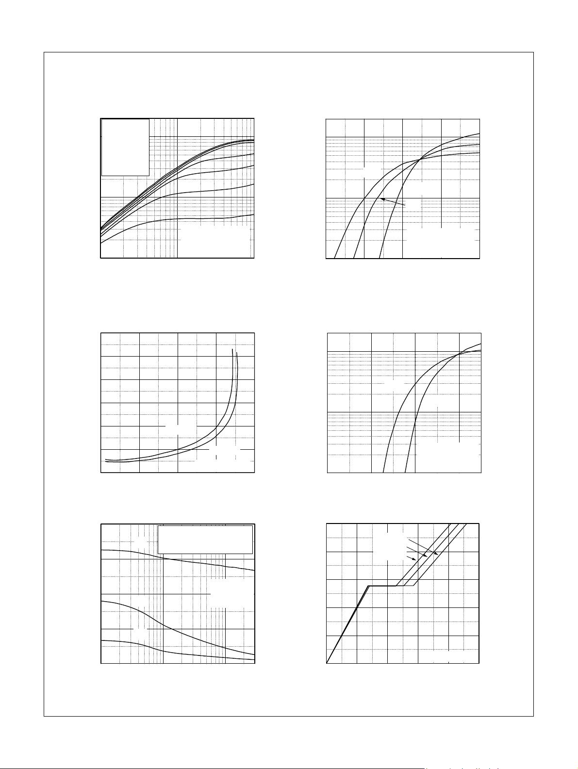
Typical Performance Characteristics
Figure 1. On-Region Characteristics Figure 2. Transfer Characteristics
200
V
= 15.0 V
GS
10.0 V
100
8.0 V
7.0 V
6.5 V
6.0 V
5.5 V
10
,Drain Current[A]
D
I
*Notes:
1. 250
µs Pulse Test
= 25oC
2. T
1
0.1 1 10
C
VDS,Drain-Source Voltage[V]
Figure 3. On-Resistance Variation vs. Figure 4. Body Diode Forward Voltage
Drain Current and Gate Voltage Variation vs. Source Current
and Temperature
0.14
0.12
200
100
150oC
-55oC
10
,Drain Current[A]
D
I
1
45678
25oC
*Notes:
1. V
= 20V
DS
2. 250µs Pulse Test
VGS,Gate-Source Voltage[V]
200
100
FDPF3860T N-Channel PowerTrench
®
MOSFET
0.10
[Ω],
0.08
DS(ON)
R
0.06
0.04
Drain-Source On-Resistance
0.02
0 25 50 75 100
VGS = 10V
*Note: TJ = 25oC
ID, Drain Current [A]
VGS = 20V
10
, Reverse Drain Current [A]
S
I
1
0.00.40.81.2
VSD, Body D io de Forward Vo lta g e [V]
150oC
25oC
*Notes:
1. VGS = 0V
2. 250
µs Pulse Test
Figure 5. Capacitance Characteristics Figure 6. Gate Charge Characteristics
2000
C
= Cgs + Cgd (Cds = shorted)
iss
C
= Cds + C
C
oss
iss
C
= C
rss
gd
1500
1000
Capacitances [pF]
500
0
0.1 1 10
C
oss
C
rss
VDS, Drain-Source Voltage [V ]
gd
*Note:
1. V
2. f = 1MHz
= 0V
GS
30
10
VDS = 80V
V
= 50V
DS
V
8
DS
= 25V
6
4
, Gate-Source Voltage [V]
GS
V
2
*Note: ID = 5.9A
0
0 5 10 15 20 25
Qg, Total Gate Charge [nC]
1.4
FDPF3860T Rev. A
3
www.fairchildsemi.com
Page 4

Typical Performance Characteristics (Continued)
Figure 7. Breakdown Voltage Variation Figure 8. On-Resistance Variation
vs. Temperature vs. Temperature
1.2
1.1
3.0
2.5
2.0
FDPF3860T N-Channel PowerTrench
1.0
, [Normalized]
DSS
BV
0.9
Drain-Source Breakdown Voltage
0.8
-100 -50 0 50 100 150 200
*Notes:
1. V
2. I
TJ, Junction Temperature [oC]
= 0V
GS
= 250µA
D
1.5
, [Normalized]
1.0
DS(on)
R
Drain-Source On-Resistance
0.5
0.0
-100 -50 0 50 100 150 200
*Notes:
1. V
2. I
TJ, Junction Temperature [oC]
GS
= 5.9A
D
= 10V
Figure 9. Maximum Safe Operating Area Figure 10. Maximum Drain Current
vs. Case Temperature
200
100
10
Operation in This Area
1
is Limited by R
, Drain Current [A]
D
I
0.1
0.01
0.1 1 10 100
DS(on)
*Notes:
= 25oC
1. T
C
2. T
= 150oC
J
3. Single Pulse
VDS, Drain-Source Voltage [V]
100µs
1ms
10ms
DC
10µs
200
25
20
15
10
, Drain Current [A]
D
I
5
0
25 50 75 100 125 150
TC, Case Temperature [oC]
Figure 11. Transient Thermal Response Curve
5
®
MOSFET
FDPF3860T Rev. A
]
Thermal Response [Z
θJC
0.1
0.01
0.5
1
0.2
0.1
0.05
0.02
0.01
Single pulse
-5
10
P
DM
t
1
t
*Notes:
1. Z
2. Duty Fact o r , D= t
3. TJM - TC = PDM * Z
-4
10
-3
10
-2
10
-1
10
0
10
2
(t) = 3.7oC/W Max.
θJC
1
10
1/t2
θJC
2
10
(t)
3
10
Rectangular Pulse Duration [sec]
4
www.fairchildsemi.com
Page 5

Gate Charge Test Circuit & Waveform
Resistive Switching Test Circuit & Waveforms
FDPF3860T N-Channel PowerTrench
®
MOSFET
FDPF3860T Rev. A
Unclamped Inductive Switching Test Circuit & Waveforms
5
www.fairchildsemi.com
Page 6

Peak Diode Recovery dv/dt Test Circuit & Waveforms
+
DUT
DUT
I
I
SD
SD
Driver
Driver
R
R
G
G
V
V
GS
GS
+
V
V
DS
DS
_
_
L
LL
Same Type
Same Type
as DUT
as DUT
• dv/dt controlled by R
• dv/dt controlled by R
•ISDcontrolled by pulse period
•ISDcontrolled by pulse period
G
G
FDPF3860T N-Channel PowerTrench
®
V
V
DD
DD
MOSFET
V
V
GS
GS
( Driver )
( Driver )
I
I
SD
SD
( DUT )
( DUT )
V
V
DS
DS
( DUT )
( DUT )
Gate Pulse Width
Gate Pulse Width
Gate Pulse Width
--------------------------
--------------------------
--------------------------
D =
D =
D =
Gate Pulse Period
Gate Pulse Period
Gate Pulse Period
IFM, Body Diode Forward Current
IFM, Body Diode Forward Current
I
I
RM
RM
Body Diode Reverse Current
Body Diode Reverse Current
Body Diode Recoverydv/dt
Body Diode Recoverydv/dt
V
V
SD
SD
Body Diode
Body Diode
Forward Voltage Drop
Forward Voltage Drop
di/dt
di/dt
10V
10V
V
V
DD
DD
FDPF3860T Rev. A
6
www.fairchildsemi.com
Page 7

Package Dimensions
0
2.54
0
FDPF3860T N-Channel PowerTrench
TO-220F
10.16 ±0.20
(7.00)
ø3.18 ±0.10
±0.20
(0.70)
3.30 ±0.1
6.68 ±0.20
(1.00x45°)
15.80 ±0.20
15.87 ±0.20
®
MOSFET
MAX1.47
0.80 ±0.10
9.75 ±0.30
(30°)
FDPF3860T Rev. A
0.35 ±0.10
2.54TYP
±0.20]
[2.54
#1
9.40 ±0.20
2.54TYP
±0.20]
[2.54
4.70 ±0.20
+0.10
0.50
–0.05
7
2.76 ±0.2
Dimensions in Millimeters
www.fairchildsemi.com
Page 8

TRADEMARKS
The following includes registered and unregistered trademarks and service marks, owned by Fairchild Semiconductor and/or its global
subsidiaries, and is not intended to be an exhaustive list of all such trademarks.
®
ACEx
Build it Now™
CorePLUS™
CorePOWER™
CROSSVOLT™
CTL™
Current Transfer Logic™
EcoSPARK
®
EfficentMax™
EZSWITCH™ *
™
®
®
Fairchild
Fairchild Semiconduct or
FACT Quiet Series™
FACT
FAST
FastvCore™
FlashWriter
®
®
® *
®
* EZSWITCH™ and FlashWriter
FPS™
F-PFS™
®
FRFET
Global Power ResourceSM
Green FPS™
Green FPS™ e-Series™
GTO™
IntelliMAX™
ISOPLANAR™
MegaBuck™
MICROCOUPLER™
MicroFET™
MicroPak™
MillerDrive™
MotionMax™
Motion-SPM™
OPTOLOGIC
OPTOPLANAR
®
®
®
®
are trademarks of System General Corporation, used under lic ens e by Fairchild Semiconduct or.
PDP SPM™
Power-SPM™
PowerTrench
Programmable Active Droop™
QFET
®
®
QS™
Quiet Series™
RapidConfigure™
Saving our world, 1mW at a time™
SmartMax™
SMART START™
®
SPM
STEALTH™
SuperFET™
SuperSOT™-3
SuperSOT™-6
SuperSOT™-8
SupreMOS™
SyncFET™
®
The Power Franchise
TinyBoost™
TinyBuck™
TinyLogic
TINYOPTO™
TinyPower™
TinyPWM™
TinyWire™
μSerDes™
UHC®
Ultra FRFET™
UniFET™
VCX™
VisualMax™
®
®
DISCLAIMER
FAIRCHILD SEMICONDUCTOR RESERVES THE RIGHT TO MAKE CHANGES WITHOUT FURTHER NOTICE TO ANY PR ODUCTS
HEREIN TO IMPROVE RELIABILITY, FUNCTION, OR DESIGN. FAIRCHILD DOES NOT ASSUME ANY LIABILITY ARISING OUT O F THE
APPLICATION OR USE OF AN Y PRODUCT OR CIRCUIT DESCRIBED HEREIN; NEITHER DOES IT CONVEY ANY LICENSE UNDER ITS
PATENT RIGHTS, NOR THE RIG HTS OF OTH ERS. THESE SPECIFICATIO NS DO N OT EXPAN D THE TERM S OF FAIRCHILD’S
WORLDWIDE TERMS AND CONDITIONS, SPECIFIC ALLY THE WARRANTY THER EIN, WHICH COVERS TH ESE PRODUCTS.
LIFE SUPPORT POLICY
FAIRCHILD’S PRODUCTS ARE NOT AUTHORIZED FOR USE AS CRITICAL COMPONENTS IN LIFE SUPPORT DEVICES OR
SYSTEMS WITHOUT THE EXPRESS WRITTEN APPROVAL OF FAIRCHILD SEMICONDUCTOR CORPORATION.
As used herein:
1. Life support devices or systems are devices or systems
which, (a) are intended for surgical im plant into the body or
(b) support or sustain lif e, and (c) whose failure to perform
when properly used in accordance with instructi ons for use
2. A critical component in any component of a life support,
device, or system whose failure to perform can be
reasonably expected to cause the fail ure of the life support
device or system, or to affect its safety or effectiveness.
provided in the labeling, can be reasonably expected to
result in a signific ant injury of the user.
PRODUCT STATUS DEFINITIONS
Definition of Terms
Datasheet Identification Product Status Definition
Advance Information Formative / In Des i gn
This datasheet contains the design specificati ons for product development.
Specifications may change in any manner without notic e.
This datasheet contains prelim inary data; supplementary data will be published
Preliminary First Production
No Identification Needed Full Production
Obsolete Not In Production
at a later date. Fairchild S emiconductor reserves the right to make changes at
any time without notice t o i mprove design.
This datasheet contains f i nal specifications. Fairchild Semiconductor reserves
the right to make changes at any time without notic e to improve the design.
This datasheet contains specifications on a product that is discontinued by
Fairchild Semiconduc tor. The datasheet is for referenc e i nformation only.
Rev. I34
© 2008 Fairchild Semiconductor Corporation www.fairchildsemi.com
 Loading...