

Page 1
FDP33N25 / FDPF33N25T
250V N-Channel MOSFET
FDP33N25 / FDPF33N25T 250V N-Channel MOSFET
October
TM
UniFET
Features
• 33A, 250V, R
• Low gate charge ( typical 36.8 nC)
• Low Crss ( typical 39 pF)
•Fast switching
• Improved dv/dt capability
G
= 0.094Ω @VGS = 10 V
DS(on)
D
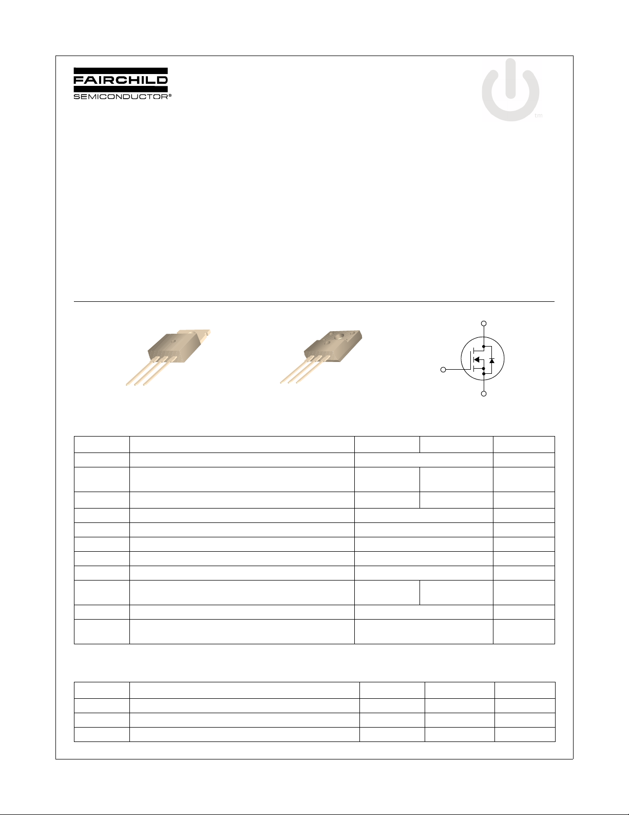
S
TO-220
FDP Series
D
G
S
Description
These N-Channel enhancement mode power field effect
transistors are produced using Fairchild’s proprietary, planar
stripe, DMOS technology.
This advanced technology has been especially tailored to
minimize on-state resistance, provide superior switching
performance, and withstand high energy pulse in the avalanche
and commutation mode. These devices are well suited for high
efficient switched mode power supplies and active power factor
correction.
D
G
TO-220F
FDPF Series
S
Absolute Maximum Ratings
Symbol Parameter FDP33N25 FDPF33N25T Unit
V
DSS
I
D
I
DM
V
GSS
E
AS
I
AR
E
AR
dv/dt Peak Diode Recovery dv/dt
P
D
T
J, TSTG
T
L
*Drain current limited by maximum junction temperature
Drain-Source Voltage 250 V
Drain Current - Continuous (TC = 25°C)
- Continuous (TC = 100°C)
Drain Current - Pulsed
Gate-Source voltage ± 30 V
Single Pulsed Avalanche Energy
Avalanche Current
Repetitive Avalanche Energy
Power Dissipation (TC = 25°C)
- Derate above 25°C
Operating and Storage Temperature Range -55 to +150 °C
Maximum Lead Temperature for Soldering Purpose,
1/8” from Case for 5 Seconds
(Note 1)
(Note 2)
(Note 1)
(Note 1)
(Note 3)
33
20.4
132 132*
918 mJ
33 A
23.5 mJ
4.5 V/ns
235
1.89
300 °C
33*
20.4*
37
0.29
A
A
A
W
W/°C
Thermal Characteristics
Symbol Parameter FDP33N25 FDPF33N25T Unit
R
θJC
R
θCS
R
θJA
©2007 Fairchild Semiconductor Corporation 1 www.fairchildsemi.com
FDP33N25 / FDPF33N25T Rev. B
Thermal Resistance, Junction-to-Case 0.53 3.4 °C/W
Thermal Resistance, Case-to-Sink Typ. 0.5 -- °C/W
Thermal Resistance, Junction-to-Ambient 62.5 62.5 °C/W
Page 2
Package Marking and Ordering Information
Device Marking Device Package Reel Size Tape Width Quantity
FDP33N25 FDP33N25 TO-220 - - 50
FDPF33N25T FDPF33N25T TO-220F - - 50
FDP33N25 / FDPF33N25T 250V N-Channel MOSFET
Electrical Characteristics T
= 25°C unless otherwise noted
C
Symbol Parameter Conditions Min Typ Max Units
Off Characteristics
BV
DSS
∆BV
/ ∆T
I
DSS
I
GSSF
I
GSSR
On Characteristics
V
GS(th)
R
DS(on)
g
FS
Dynamic Characteristics
C
iss
C
oss
C
rss
Switching Characteristics
t
d(on)
t
r
t
d(off)
t
f
Q
g
Q
gs
Q
gd
Drain-Source Diode Characteristics and Maximum Ratings
I
S
I
SM
V
SD
t
rr
Q
rr
Notes:
1. Repetitive Rating: Pulse width limited by maximum junction temperature
2. L = 1.35mH, IAS = 33A, VDD = 50V, RG = 25Ω, Starting TJ = 25°C
3. ISD ≤ 33A, di/dt ≤ 200A/µs, VDD ≤ BV
4. Pulse Test: Pulse width ≤ 300µs, Duty Cycle ≤ 2%
5. Essentially Independent of Operating Temperature Typical Characteristics
Drain-Source Breakdown Voltage VGS = 0V, ID = 250µA, TJ = 25°C 250 -- -- V
Breakdown Voltage Temperature
DSS
Coefficient
J
Zero Gate Voltage Drain Current VDS = 250V, VGS = 0V
ID = 250µA, Referenced to 25°C -- 0.25 -- V/°C
VDS = 200V, TC = 125°C
--
--
--
-Gate-Body Leakage Current, Forward VGS = 30V, VDS = 0V -- -- 100 nA
Gate-Body Leakage Current, Reverse VGS = -30V, VDS = 0V -- -- -100 nA
Gate Threshold Voltage VDS = VGS, ID = 250µA 3.0 -- 5.0 V
Static Drain-Source
On-Resistance
VGS = 10V, ID = 16.5A -- 0.077 0.094 Ω
Forward Transconductance VDS = 40V , ID = 16.5A (Note 4) -- 26.6 -- S
Input Capacitance VDS = 25V, VGS = 0V,
Output Capacitance -- 330 430 pF
f = 1.0MHz
-- 1640 2135 pF
Reverse Transfer Capacitance -- 39 59 pF
Turn-On Delay Time VDD = 125V, ID = 33A
Turn-On Rise Time -- 230 470 ns
RG = 25Ω
-- 35 80 ns
Turn-Off Delay Time -- 75 160 ns
Turn-Off Fall Time -- 120 250 ns
Total Gate Charge VDS = 200V, ID = 33A
Gate-Source Charge -- 10 -- nC
VGS = 10V
Gate-Drain Charge -- 17 -- nC
(Note 4, 5)
-- 36.8 48 nC
(Note 4, 5)
Maximum Continuous Drain-Source Diode Forward Current -- -- 33 A
Maximum Pulsed Drain-Source Diode Forward Current -- -- 132 A
Drain-Source Diode Forward Voltage VGS = 0V, IS = 33A -- -- 1.4 V
Reverse Recovery Time VGS = 0V, IS = 33A
Reverse Recovery Charge -- 1.71 -- µC
, Starting TJ = 25°C
DSS
dIF/dt =100A/µs (Note 4)
-- 220 -- ns
10
1
µA
µA
FDP33N25 / FDPF33N25T Rev. B
2 www.fairchildsemi.com
Page 3
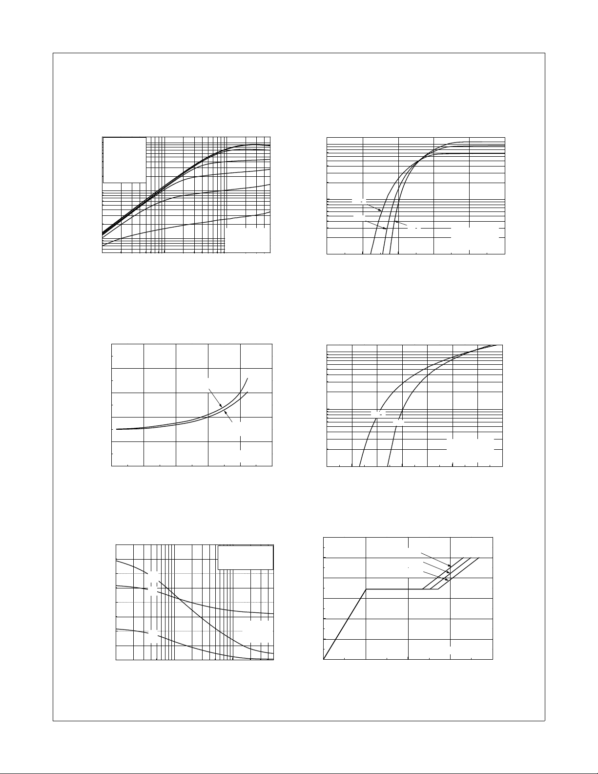
Typical Performance Characteristics
Figure 1. On-Region Characteristics Figure 2. Transfer Characteristics
FDP33N25 / FDPF33N25T 250V N-Channel MOSFET
10
10
, Drain Current [A]
D
I
10
2
V
Top : 15.0 V
10.0 V
8.0 V
7.0 V
6.5 V
6.0 V
Bottom : 5.5 V
1
0
-1
10
GS
0
10
VDS, Drain-Source Voltage [V]
2
10
1
10
, Drain Current [A]
D
I
10
150oC
25oC
0
24681012
10
* Notes :
1. 250
2. T
1
µs Pulse Test
= 25oC
C
VGS, Gate-Source Voltage [V]
-55oC
* Notes :
= 40V
1. V
DS
µs Pulse Test
2. 250
Figure 3. On-Resistance Variation vs. Figure 4. Body Diode Forward Voltage
Drain Current and Gate Voltage Variation vs. Source Current
and Temperatue
0.25
0.20
VGS = 10V
0.15
[Ω],
DS(ON)
0.10
R
0.05
Drain-Sour ce On-Resist an ce
0.00
0 20 40 60 80 100
ID, Drain Current [A]
VGS = 20V
* Note : TJ = 25oC
2
10
1
10
, Reverse Drain Current [A]
DR
I
0
10
0.20.40.60.81.01.21.41.6
150oC
VSD, Source-Drain voltage [V]
25oC
* Notes :
1. V
= 0V
GS
µs Pulse Test
2. 250
Figure 5. Capacitance Characteristics Figure 6. Gate Charge Characteristics
4000
Capacitances [pF]
3000
2000
1000
0
-1
10
C
oss
C
iss
C
rss
VDS, Drain-Source Voltage [V]
FDP33N25 / FDPF33N25T Rev. B
C
= Cgs + Cgd (Cds = shorte d )
iss
C
= Cds + C
oss
gd
C
= C
rss
gd
* Note :
1. V
= 0 V
GS
2. f = 1 MHz
0
10
1
10
12
10
8
VDS = 50V
VDS = 125V
VDS = 200V
6
4
, Gate-Sourc e Voltage [V]
2
GS
V
0
0 10203040
QG, Total Gate Ch a rg e [nC]
3 www.fairchildsemi.com
* Note : ID = 33A
Page 4

Typical Performance Characteristics (Continued)
Figure 7. Breakdown Voltage Variation Figure 8. On-Resistance Variation
vs. Temperature vs. Temperature
FDP33N25 / FDPF33N25T 250V N-Channel MOSFET
1.2
3.0
2.5
1.1
2.0
1.0
, (Normalized)
BV
DSS
0.9
* Notes :
1. V
2. I
Drain-Source Breakdown Voltage
0.8
-100 -50 0 50 100 150 200
TJ, Junction Temperature [oC]
= 0 V
GS
= 250 µA
D
1.5
, (Normalized)
1.0
DS(ON)
R
0.5
Drain-Source On-Resistance
0.0
-100 -50 0 50 100 150 200
TJ, Junction Temperature [oC]
* Notes :
1. V
2. I
= 10 V
GS
= 16.5 A
D
Figure 9-1. Maximum Safe Operating Area Figure 9-2. Maximum Safe Operating Area
for FDP33N25 for FDPF33N25T
, Drain Current [A]
D
I
2
10
10 µs
2
10
100 µs
1 ms
1
10
10
10
0
-1
10
0
Operation in This Area
is Limited by R
DS(on)
1
10
10 ms
100 ms
DC
1
10
Operation in This Area
is Limited by R
DS(on)
* Notes :
= 25 oC
1. T
C
2. T
= 150 oC
J
3. Single Pulse
2
10
, Drain Current [A]
D
I
0
10
-1
10
0
10
VDS, Dra in-Sourc e Voltag e [V]
1 ms
10 ms
100 ms
DC
* Notes :
= 25 oC
1. T
C
= 150 oC
2. T
J
3. Single Pulse
1
10
VDS, Drain-Source Voltage [V]
100 µs
10
10 µs
2
Figure 10. Maximum Drain Current
vs. Case Temperature
40
30
20
, Drain Current [A]
D
I
10
0
25 50 75 100 125 150
TC, Case Temperature [oC]
FDP33N25 / FDPF33N25T Rev. B
4 www.fairchildsemi.com
Page 5

Typical Performance Characteristics (Continued)
Figure 11-1. Transient Thermal Response Curve for FDP33N25
0
10
D=0.5
-1
0.2
10
0.1
0.05
0.02
0.01
-2
10
(t), Thermal Response
θJC
Z
single pulse
P
DM
t
1
t
* Notes :
1. Z
2. Duty Fa ctor, D=t
3. TJM - TC = PDM * Z
2
(t) = 0.53 oC/W Max.
θJC
FDP33N25 / FDPF33N25T 250V N-Channel MOSFET
1/t2
(t)
θJC
-5
10
-4
10
-3
10
-2
10
-1
10
0
10
1
10
t1, Square W ave Pulse Duration [sec]
Figure 11-2. Transient Thermal Response Curve for FDPF33N25T
D=0.5
0
10
0.2
0.1
(t), Thermal Resp onse
θJC
Z
0.05
-1
10
0.02
0.01
-2
10
-5
10
single pulse
-4
10
-3
10
10
t1, Squ a re Wave P u lse D u ra tio n [ se c ]
-2
P
DM
t
1
t
(t) = 3.4 oC/W Max.
θJC
-1
10
2
* Notes :
1. Z
2. Duty Fa c to r, D=t
3. TJM - TC = PDM * Z
1/t2
(t)
θJC
0
10
1
10
FDP33N25 / FDPF33N25T Rev. B
5 www.fairchildsemi.com
Page 6

Gate Charge Test Circuit & Waveform
Resistive Switching Test Circuit & Waveforms
FDP33N25 / FDPF33N25T 250V N-Channel MOSFET
FDP33N25 / FDPF33N25T Rev. B
Unclamped Inductive Switching Test Circuit & Waveforms
6 www.fairchildsemi.com
Page 7

Peak Diode Recovery dv/dt Test Circuit & Waveforms
FDP33N25 / FDPF33N25T 250V N-Channel MOSFET
FDP33N25 / FDPF33N25T Rev. B
7 www.fairchildsemi.com
Page 8

Mechanical Dimensions
FDP33N25 / FDPF33N25T 250V N-Channel MOSFET
TO-220
FDP33N25 / FDPF33N25T Rev. B
Dimensions in Millimeters
8 www.fairchildsemi.com
Page 9

Package Dimensions
FDP33N25 / FDPF33N25T 250V N-Channel MOSFET
TO-220F Potte d
* Front/Back Side Isolation Voltage : AC 2500V
FDP33N25 / FDPF33N25T Rev. B
Dimensions in Millimeters
Dimensions in Millimeters
9 www.fairchildsemi.com
Page 10

TRADEMARKS
tm
®
tm
tm
The following includes registered and unregistered trademarks and service marks, owned by Fairchild S emiconductor and/or its gl obal subsidiaries, a nd is not
intended to be an exhaustive list of all such trademarks.
AccuPower™
Auto-SPM™
Build it Now™
CorePLUS™
CorePOWER™
CROSSVOLT™
CTL™
Current Transfer Logic™
EcoSPARK
EfficentMax™
EZSWITCH™*
™*
Fairchild
Fairchild Semiconductor
FACT Quiet Series™
FACT
FAST
FastvCore™
FETBench™
FlashWriter
®
®
®
®
®
*
®
FPS™
F-PFS™
FRFET
Global Power Resource
Green FPS™
Green FPS™ e-Series™
Gmax™
GTO™
IntelliMAX™
ISOPLANAR™
MegaBuck™
MICROCOUPLER™
MicroFET™
MicroPak™
MillerDrive™
MotionMax™
Motion-SPM™
OPTOLOGIC
OPTOPLANAR
®
PDP SPM™
Power-SPM™
PowerTrench
®
®
SM
®
PowerXS™
Programmable Active Droop™
QFET
QS™
Quiet Series™
RapidConfigure™
Saving our world, 1mW /W /kW at a time™
SmartMax™
SMART START™
SPM
STEALTH™
SuperFET™
SuperSOT™-3
SuperSOT™-6
SuperSOT™-8
SupreMOS™
SyncFET™
Sync-Lock™
®
®
™
®
®*
The Power Franchise
®
TinyBoost™
TinyBuck™
TinyCalc™
®
TinyLogic
TINYOPTO™
TinyPower™
TinyPWM™
TinyWire™
TriFault Detect™
TRUECURRENT™*
®
UHC
Ultra FRFET™
UniFET™
VCX™
VisualMax™
XS™
®
*Trademarks of System General Corporation, used under license by Fairchild Semiconductor.
DISCLAIMER
FAIRCHILD SEMICONDUCTOR RESERVES THE RIGHT TO MAKE CHANGES WITHOUT FURTHER NOTICE TO ANY PRODUCTS HEREIN TO IMPROVE
RELIABILITY, FUNCTION, OR DESIGN. FAIRCHILD DOES NOT ASSUME ANY LIABILITY ARISING OUT OF THE APPLICATION OR USE OF ANY
PRODUCT OR CIRCUIT DESCRIBED HEREIN; NEITHER DOES IT CONVEY ANY LICENSE UNDER ITS PATENT RIGHTS, NOR THE RIGHTS OF OTHERS.
THESE SPECIFICATIONS DO NOT EXPAND THE TERMS OF FAIRCHILD’S WORLDWIDE TERMS AND CONDITIONS, SPECIFICALLY THE WARRANTY
THEREIN, WHICH COVERS THESE PRODUCTS.
FDP33N25 / FDPF33N25T 250V N-Channel MOSFET
LIFE SUPPORT POLICY
FAIRCHILD’S PRODUCTS ARE NOT AUTHORIZED FOR USE AS CRITICAL COMPONENTS IN LIFE SUPPORT DEVICES OR SYSTEMS WITHOUT THE
EXPRESS WRITTEN APPROVAL OF FAIRCHILD SEMICONDUCTOR CORPORATION.
As used herein:
1. Life support devices or systems are devices or systems which, (a) are
intended for surgical implant into the bo dy or (b ) sup port or sust ain li fe,
and (c) whose failure to perform when properly used in accordance with
instructions for use provided in the labeling, can be reasonably
expected to result in a significant injury of the user.
ANTI-COUNTERFEITING POLICY
Fairchild Semiconductor Corporation’s Anti-Counterfeiting Policy. Fairchild’s Anti-Counterfeiting Policy is also stated on our external website,
www.Fairchildsemi.com, under Sales Support
Counterfeiting of semiconductor parts is a growing problem in the industry. Al l manufactures of semiconductor products are exper iencing counterfeiting of th eir
parts. Customers who inadvertently purchase counterfeit parts experience many probl ems such a s loss of brand rep uta tion, subst andard performance, failed
application, and increased cost of production and manufacturing delays. Fairchil d is taking st rong measures to prote ct ourselve s and our customers from the
proliferation of counterfeit parts. Fairchild st rongly encourages customers to purchase Fairchild parts either directly from Fairchild or from Authorized Fairchild
Distributors who are listed by country on our web page cited above. Products customers buy either from Fairchild directly or from Authorized Fairchild
Distributors are genuine parts, have full traceability, meet Fairchild’s quality standards for handing and storage and provide access to Fairchild’s full range of
up-to-date technical and product information. Fairchild and our Authorized Distributors will stand behind all warranties and will appropriately address and
warranty issues that may arise. Fairchild will not provide any warranty coverage or other assistance for parts bought from Unauthorized Sources. Fairchild is
committed to combat this global problem and encourage our customers to do their part in stopping this practi ce by buying direct or from aut horized distributors.
PRODUCT STATUS DEFINITIONS
Definition of Terms
.
2. A critical component in any component of a life support, device, or
system whose failure to perform can be reasonably expected to cause
the failure of the life support device or system, or to affect its safety or
effectiveness.
Datasheet Identification Product Status Definition
Advance Information Formative / In Design
Preliminary First Production
No Identification Needed Full Production
Obsolete Not In Production
Datasheet contains the design specifications for product development. Specifications
may change in any manner without notice.
Datasheet contains preliminary data; supplementary data will be published at a later
date. Fairchild Semiconductor reserves the right to make changes at any time without
notice to improve design.
Datasheet contains final specifications. Fairchild Semiconductor reserves the right to
make changes at any time without notice to improve the design.
Datasheet contains specifications on a product that is discontinued by Fairchild
Semiconductor. The datash eet is for reference information only.
Rev. I41
10 www.fairchildsemi.com10 www.fairchildsemi.com
FDP33N25 / FDPF33N25T Rev. B
 Loading...