

Page 1
FDPF2710T
250V N-Channel PowerTrench MOSFET
FDPF2710T 250V N-Channel PowerTrench MOSFET
September 2007
General Description
This N-Channel MOSFET is produced using Fairchild Semiconductor’s advanced PowerTrench process that has been especially tailored to minimize the on-state resistance and yet
maintain superior switching performance.
Description
• 25A, 250V, R
• Fast switching speed
• Low gate charge
• High performance trench technology for extremely low R
• High power and current handling capability
= 36.3mΩ @VGS = 10 V
DS(on)
Application
• Ballast Application
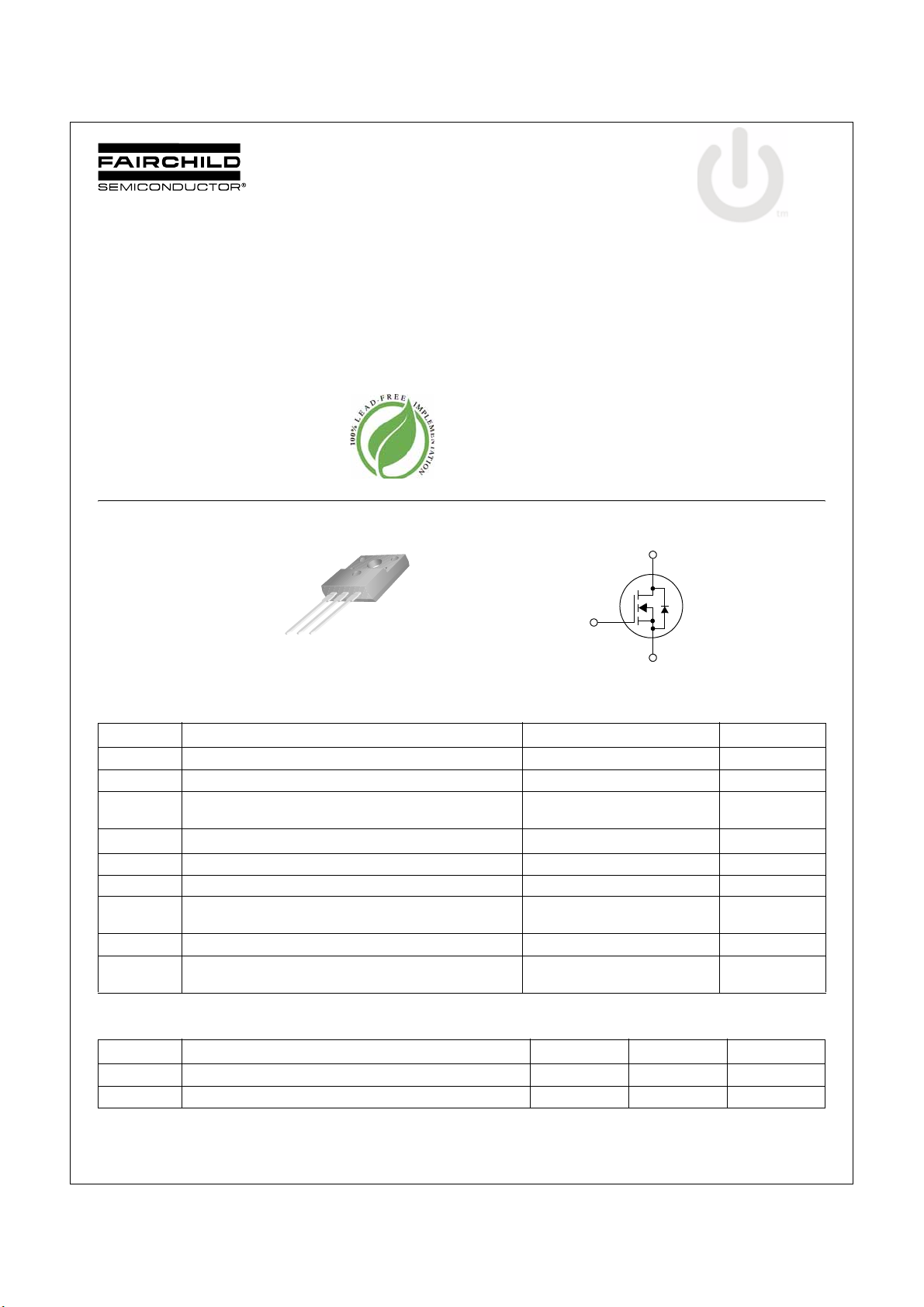
D
G
D
G
S
TO-220F
S
Absolute Maximum Ratings
Symbol Parameter Ratings Unit
V
DS
V
GS
I
D
I
DM
E
AS
dv/dt Peak Diode Recovery dv/dt
P
D
T
J, TSTG
T
L
Drain-Source Voltage 250 V
Gate-Source voltage ± 30 V
Drain Current - Continuous (TC = 25°C)
- Continuous (T
Drain Current - Pulsed
Single Pulsed Avalanche Energy
Power Dissipation (TC = 25°C)
- Derate above 25°C
Operating and Storage Temperature Range -55 to +150 °C
Maximum Lead Temperature for Soldering Purpose,
1/8” from Case for 5 Seconds
= 100°C)
C
(Note 1)
(Note 2)
(Note 3) 4.5 V/ns
25
18.8
100
145 mJ
62.5
0.5
300 °C
DS(on)
A
A
A
W
W/°C
Thermal Characteristics
Symbol Parameter Min Max Unit
R
θJC
R
θJA
©2007 Fairchild Semiconductor Corporation 1 www.fairchildsemi.com
FDPF2710T Rev. A
Thermal Resistance, Junction-to-Case -- 2.0 °C/W
Thermal Resistance, Junction-to-Ambient -- 62.5 °C/W
Page 2
Package Marking and Ordering Information
Device Marking Device Package Reel Size Tape Width Quantity
FDPF2710T FDPF2710T TO-220F -- -- 50
FDPF2710T 250V N-Channel PowerTrench MOSFET
Electrical Characteristics T
= 25°C unless otherwise noted
C
Symbol Parameter Conditions Min Typ Max Units
Off Characteristics
BV
DSS
∆BV
/ ∆T
I
DSS
I
GSSF
I
GSSR
On Characteristics
V
GS(th)
R
DS(on)
g
FS
Dynamic Characteristics
C
iss
C
oss
C
rss
Switching Characteristics
t
d(on)
t
r
t
d(off)
t
f
Q
g
Q
gs
Q
gd
Drain-Source Diode Characteristics and Maximum Ratings
I
S
I
SM
V
SD
t
rr
Q
rr
Drain-Source Breakdown Voltage VGS = 0V, ID = 250µA, TJ = 25°C 250 -- -- V
Breakdown Voltage Temperature
DSS
Coefficient
J
Zero Gate Voltage Drain Current VDS = 250V, VGS = 0V
I
= 250µA, Referenced to 25°C--0.25--V/°C
D
= 250V, VGS = 0V,TC = 125°C
V
DS
--
--
--
-Gate-Body Leakage Current, Forward VGS = 30V, VDS = 0V -- -- 100 nA
Gate-Body Leakage Current, Reverse VGS = -30V, VDS = 0V -- -- -100 nA
Gate Threshold Voltage VDS = VGS, ID = 250µA 3.0 3.9 5.0 V
Static Drain-Source On-Resistance VGS = 10V, ID = 25A -- 36.3 42.5 mΩ
Forward Transconductance VDS = 10V, ID = 25A
Input Capacitance
= 25V, VGS = 0V,
V
Output Capacitance -- 426 567 pF
Reverse Transfer Capacitance -- 97 146 pF
DS
f = 1.0MHz
Turn-On Delay Time VDD = 125V, ID = 50A
V
= 10V, R
Turn-On Rise Time -- 252 514 ns
GS
GEN
= 25Ω
(Note 4)
-- 63 -- S
-- 5470 7280 pF
-- 80 170 ns
Turn-Off Delay Time -- 112 234 ns
Turn-Off Fall Time -- 154 318 ns
Total Gate Charge VDS = 125V, ID = 50A
= 10V
V
Gate-Source Charge -- 34 -- nC
GS
Gate-Drain Charge -- 18 -- nC
(Note 4, 5)
-- 78 101 nC
(Note 4, 5)
Maximum Continuous Drain-Source Diode Forward Current -- -- 25 A
Maximum Pulsed Drain-Source Diode Forward Current -- -- 150 A
Drain-Source Diode Forward Voltage VGS = 0V, IS = 25A -- -- 1 . 2 V
Reverse Recovery Time VGS = 0V, IS = 50A
dI
/dt =130A/µs (Note 4)
Reverse Recovery Charge -- 1.3 -- µC
F
-- 163 -- ns
10
500µAµA
Notes:
1. Repetitive Rating: Pulse width limited by maximum junction temperature
2. L = 1mH, I
3. ISD ≤ 50A, di/dt ≤ 200A/µs, VDD ≤ BV
4. Pulse Test: Pulse width ≤ 300µs, Duty Cycle ≤ 2%
5. Essentially Independent of Operating Temperature Typical Characteristics
= 17A, VDD = 50V, RG = 25Ω, Starting TJ = 25°C
AS
, Starting TJ = 25°C
DSS
FDPF2710T Rev. A
2 www.fairchildsemi.com
Page 3
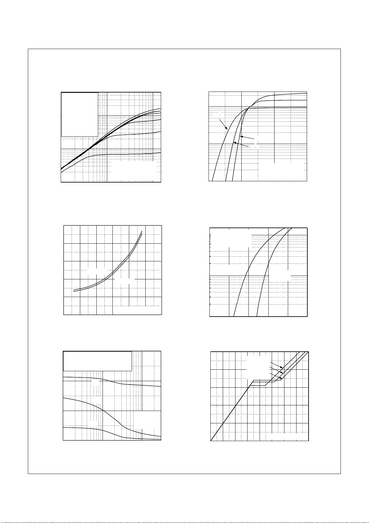
Typical Performance Characteristics
Figure 1. On-Region Characteristics Figure 2. Transfer Characteristics
500
100
V
Top : 15.0 V
10.0 V
8.0 V
7.0 V
6.5 V
6.0 V
Bottom : 5.5 V
GS
10
,Drain Current[A]
D
I
* Notes :
1. 250
µs Pulse Test
2. T
= 25oC
1
0.1 1 10
VDS,Drain-Source Voltage[V]
C
Figure 3. On-Resistance Variation vs. Figure 4. Body Diode Forward Voltage
Drain Current and Gate Voltage Variation vs. Source Current
and Temperatue
0.07
0.06
250
100
150oC
10
,Drain Current[A]
D
I
1
46810
25oC
-55oC
* Notes :
1. V
DS
2. 250
= 20V
µs Pulse Test
VGS,Gate-Source Voltage[V]
150
* Notes :
100
1. V
=0V
GS
2. 250
µs Pulse Test
FDPF2710T 250V N-Channel PowerTrench MOSFET
0.05
[Ω],
0.04
DS(ON)
R
VGS = 10V
VGS = 20V
0.03
Drain-Source On-Resistance
0.02
0 255075100125150
* Note : TJ = 25oC
ID, Drain Current [A]
10
, Reverse Drain Current [A]
S
I
TA = 150oC
1
0.20.40.60.81.01.2
TA = 25oC
VSD, Body Diode Forward Voltage [V]
Figure 5. Capacitance Characteristics Figure 6. Gate Charge Characteristics
Capacitances [pF]
9000
6000
3000
C
= Cgs + Cgd (Cds = shorted)
iss
C
= Cds + C
oss
C
= C
rss
gd
0
-1
10
VDS, Drain-Source Voltage [V]
gd
C
iss
C
oss
* Note:
1. V
= 0V
C
rss
0
10
GS
2. f = 1MHz
1
10
30
10
VDS = 50V
V
= 125V
8
V
DS
DS
= 200V
6
4
, Gate-Source Voltage [V]
GS
V
2
0
0 1020304050607080
* Note : ID = 50A
Qg, Total Gate Charge [nC]
FDPF2710T Rev. A
3 www.fairchildsemi.com
Page 4

Typical Performance Characteristics (Continued)
Figure 7. Breakdown Voltage Variation Figure 8. On-Resistance Variation
vs. Temperature vs. Temperature
1.2
2.5
FDPF2710T 250V N-Channel PowerTrench MOSFET
1.1
2
1.0
, [Normalized]
DSS
BV
0.9
* Notes :
Drain-Source Breakdown Voltage
1. V
2. I
0.8
-100 -50 0 50 100 150 200
TJ, Junction Temperature [oC]
= 0V
GS
= 250µA
D
, [Normalized]
1
DS(on)
r
Drain-Source On-Resistance
0
-100 -50 0 50 100 150 200
* Notes :
1. V
2. I
TJ, Junction Temperature [oC]
Figure 9. Maximum Safe Operating Area Figure 10. Maximum Drain Current
vs. Case Temperature
100
10
[A]
D
Operation in This Area
1
is Limited by R
Drain Current, I
0.1
0.01
* Notes :
= 25oC
1. T
C
= 150oC
2. T
J
3. Single Pulse
110100
Drain-Source Voltage, VDS [V]
DS(on)
30
100µs
1ms
10 ms
DC
400
20
10
, Drain Current [A]
D
I
0
25 50 75 100 125 150
T
, Case Temperature [oC]
C
GS
= 25A
D
= 10V
Figure 11. Transient Thermal Response Curve
0
10
]
0.5
θJC
FDPF2710T Rev. A
0.2
0.1
-1
10
0.05
0.02
0.01
-2
10
Thermal Response [Z
Single pulse
-3
10
-5
10
-4
10
-3
10
-2
10
10
Rectangular Pulse Duration [sec]
4 www.fairchildsemi.com
P
DM
* Notes :
1. Z
θJC
2. Duty Factor, D=t
3. TJM - TC = PDM * Z
-1
10
t
1
(t) = 2.0oC/W Max.
0
t
2
1/t2
(t)
θJC
1
10
2
10
Page 5

Gate Charge Test Circuit & Waveform
Resistive Switching Test Circuit & Waveforms
FDPF2710T 250V N-Channel PowerTrench MOSFET
FDPF2710T Rev. A
Unclamped Inductive Switching Test Circuit & Waveforms
5 www.fairchildsemi.com
Page 6

Peak Diode Recovery dv/dt Test Circuit & Waveforms
FDPF2710T 250V N-Channel PowerTrench MOSFET
FDPF2710T Rev. A
6 www.fairchildsemi.com
Page 7

Package Dimensions
FDPF2710T 250V N-Channel PowerTrench MOSFET
TO-220F Potted
* Front/Back Side Isolation Voltage : AC 2500V
FDPF2710T Rev. A
Dimensions in Millimeters
7
www.fairchildsemi.com
Page 8

TRADEMARKS
®
The following are registered and unregistered trademarks and service marks Fairchild Semiconductor owns or is authorized to use and is
not intended to be an exhaustive list of all such trademarks.
®
ACEx
Build it Now™
CorePLUS™
CROSSVOLT™
CTL™
Current Transfer Logic™
EcoSPARK
Fairchild
®
®
Fairchild Semiconductor
FACT Quiet Series™
®
FACT
®
FAST
FastvCore™
FPS™
®
FRFET
Global Power Resource
Green FPS™
Green FPS™ e-Series™
GTO™
i-Lo™
IntelliMAX™
ISOPLANAR™
MegaBuck™
MICROCOUPLER™
®
MicroFET™
MicroPak™
MillerDrive™
Motion-SPM™
OPTOLOGIC
OPTOPLANAR
®
SM
PDP-SPM™
Power220
®
®
®
Power247
POWEREDGE
Power-SPM™
PowerTrench
Programmable Active Droop™
QFET
QS™
QT Optoelectronics™
Quiet Series™
RapidConfigure™
SMART START™
SPM
STEALTH™
SuperFET™
SuperSOT™-3
SuperSOT™-6
®
®
®
®
SuperSOT™-8
SyncFET™
The Power Franchise
TinyBoost™
TinyBuck™
TinyLogic
®
®
TINYOPTO™
TinyPower™
®
TinyPWM™
TinyWire™
µSerDes™
®
UHC
UniFET™
VCX™
FDPF2710T 250V N-Channel PowerTrench MOSFET
DISCLAIMER
FAIRCHILD SEMICONDUCTOR RESERVES THE RIGHT TO MAKE CHANGES WITHOUT FURTHER NOTICE TO ANY PRODUCTS
HEREIN TO IMPROVE RELIABILITY, FUNCTION, OR DESIGN. FAIRCHILD DOES NOT ASSUME ANY LIABILITY ARISING OUT OF THE
APPLICATION OR USE OF ANY PRODUCT OR CIRCUIT DESCRIBED HEREIN; NEITHER DOES IT CONVEY ANY LICENSE UNDER
ITS PATENT RIGHTS, NOR THE RIGHTS OF OTHERS. THESE SPECIFICATIONS DO NOT EXPAND THE TERMS OF FAIRCHILD’S
WORLDWIDE TERMS AND CONDITIONS, SPECIFICALLY THE WARRANTY THEREIN, WHICH COVERS THESE PRODUCTS.
LIFE SUPPORT POLICY
FAIRCHILD’S PRODUCTS ARE NOT AUTHORIZED FOR USE AS CRITICAL COMPONENTS IN LIFE SUPPORT DEVICES OR
SYSTEMS WITHOUT THE EXPRESS WRITTEN APPROVAL OF FAIRCHILD SEMICONDUCTOR CORPORATION.
As used herein:
1. Life support devices or systems are devices or systems
which, (a) are intended for surgical implant into the body or (b)
support or sustain life, and (c) whose failure to perform when
properly used in accordance with instructions for use provided
2. A critical component in any component of a life support,
device, or system whose failure to perform can be reasonably
expected to cause the failure of the life support device or
system, or to affect its safety or effectiveness.
in the labeling, can be reasonably expected to result in a
significant injury to the user.
PRODUCT STATUS DEFINITIONS
Definition of Terms
Datasheet Identification Product Status Definition
Advance Information Formative or In Design
This datasheet contains the design specifications for product
development. Specifications may change in any manner without notice.
This datasheet contains preliminary data; supplementary data will be pub-
Preliminary First Production
lished at a later date. Fairchild Semiconductor reserves the right to make
changes at any time without notice to improve design.
No Identification Needed Full Production
This datasheet contains final specifications. Fairchild Semiconductor reserves
the right to make changes at any time without notice to improve design.
This datasheet contains specifications on a product that has been discontin-
Obsolete Not In Production
ued by Fairchild Semiconductor. The datasheet is printed for reference information only.
Rev. I31
FDPF2710T Rev. A
8 www.fairchildsemi.com
 Loading...