

Page 1
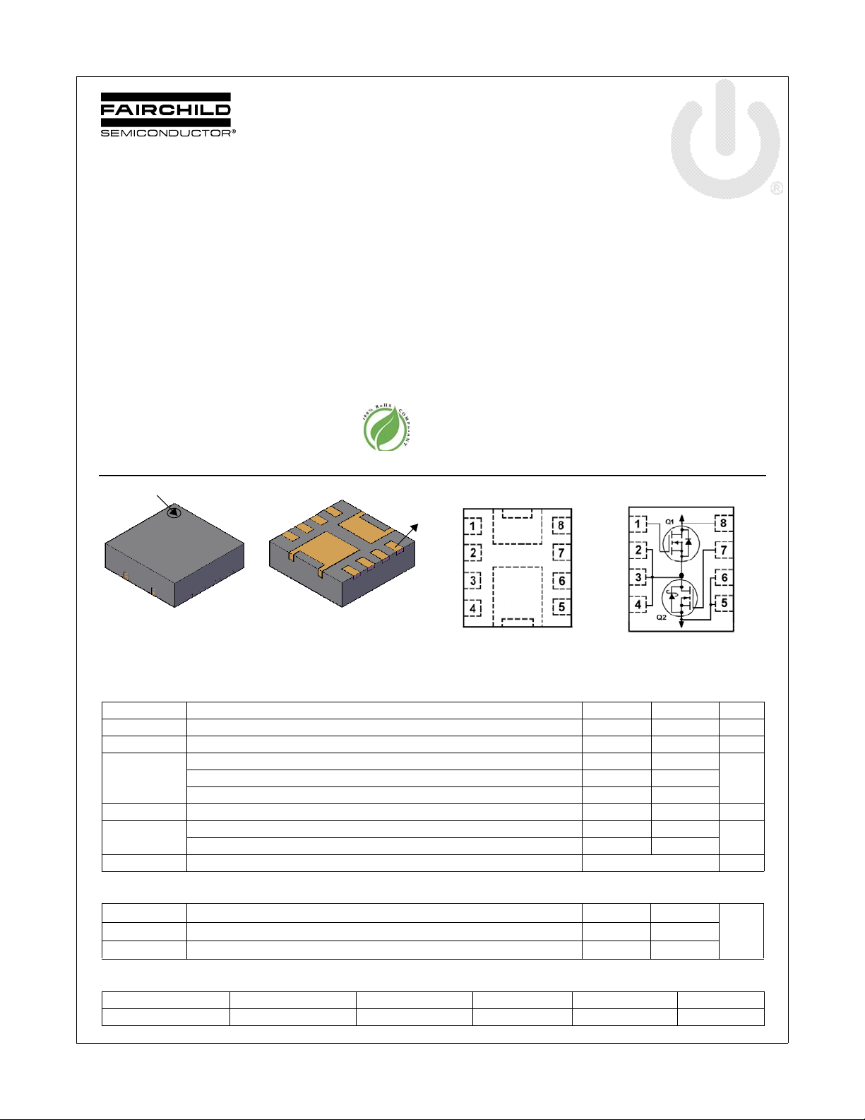
FDPC8013S
PowerTrench
30 V Asymmetric Dual N-Channel MOSFET
Features
Q1: N-Channel
Max r
Q2: N-Channel
Max r
Low inductance packaging shortens rise/fall times, resulting in
lower switching losses
MOSFET integration enables optimum layout for lower circuit
inductance and reduced switch node ringing
RoHS Compliant
= 9.6 mΩ at VGS = 4.5 V, ID = 10 A
DS(on)
= 2.7 mΩ at VGS = 4.5 V, ID = 22 A
DS(on)
®
Power Clip
General Description
This device includes two specialized N-Channel MOSFETs in a
dual package. The switch node has been internally connected to
enable easy placement and routing of synchronous buck
converters. The control MOSFET (Q1) and synchronous
TM
SyncFET
(Q2) have been designed to provide optimal power
efficiency.
Applications
Computing
Communications
General Purpose Point of Load
April 2012
FDPC8013S PowerTrench
®
Power Clip
Pin 1
GND
Top
3.3 mm x 3.3 mm
MOSFET Maximum Ratings T
GND
LS
V+
V+
(HSD
GND
(LSS
SW
SW
Bottom
= 25 °C unless otherwise noted
A
SW
Pin 1
HSG
HSG
SW
SW
SW
PAD9
V+(HSD)
PAD10
GND(LSS)
V+
LSG
GND
GND
HSG
SW
SW
SW
SW
Symbol Parameter Q1 Q2 Units
V
DS
V
GS
Drain to Source Voltage 30 30 V
Gate to Source Voltage (Note 4) ±20 ±20 V
Drain Current -Continuous (Package limited) TC = 25 °C 20 55
I
D
= 25 °C 13
A
1a
26
1b
-Pulsed 40 100
E
AS
P
D
TJ, T
STG
Single Pulse Avalanche Energy (Note 3) 21 97 mJ
Power Dissipation for Single Operation TA = 25 °C 1.6
Power Dissipation for Single Operation T
= 25 °C 0.8
A
1a
1c
2.0
0.9
1b
1d
Operating and Storage Junction Temperature Range -55 to +150 °C
Thermal Characteristics
R
θJA
θJA
R
θJC
Thermal Resistance, Junction to Ambient 77
Thermal Resistance, Junction to Ambient 151
Thermal Resistance, Junction to Case 5.0 3.5
1a
1c
63
135
1b
1d
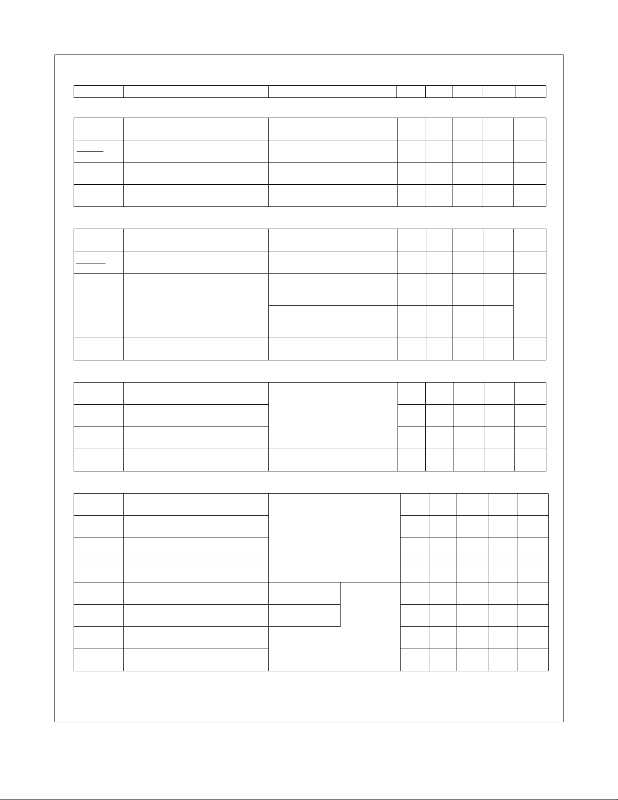
Package Marking and Ordering Information
V+
LSG
GND
GND
A -Continuous T
W
°C/WR
Device Marking Device Package Reel Size Tape Width Quantity
13CF/15CF FDPC8013S Power Clip 33 13 ” 12 mm 3000 units
©2012 Fairchild Semiconductor Corporation
FDPC8013S Rev.C1
1
www.fairchildsemi.com
Page 2
FDPC8013S PowerTrench
Electrical Characteristics T
= 25 °C unless otherwise noted
J
Symbol Parameter Test Conditions Type Min Typ Max Units
Off Characteristics
BV
ΔBV
ΔT
I
DSS
I
GSS
DSS
DSS
J
Drain to Source Breakdown Voltage
Breakdown Voltage Temperature
Coefficient
Zero Gate Voltage Drain Current
Gate to Source Leakage Current,
Forward
= 250 μA, VGS = 0 V
D
I
= 1 mA, VGS = 0 V
D
ID = 250 μA, referenced to 25 °C
I
= 10 mA, referenced to 25 °C
D
V
DS
V
DS
= 24 V, V
= 24 V, V
GS
GS
= 0 V
= 0 V
VGS = 20 V, VDS= 0 V
V
= 20 V, VDS= 0 V
GS
Q1Q230
30
Q1
Q2
Q1
Q2
Q1
Q2
V
16
20
500
100
100
mV/°C
1
I
On Characteristics
V
V
GS(th)
ΔV
ΔT
r
DS(on)
g
FS
GS(th)
J
Gate to Source Threshold Voltage
Gate to Source Threshold Voltage
Temperature Coefficient
Drain to Source On Resistance
Forward Transconductance
= VDS, ID = 250 μA
GS
V
= VDS, ID = 1 mA
GS
ID = 250 μA, referenced to 25 °C
I
= 10 mA, referenced to 25 °C
D
V
= 10 V, ID = 13 A
GS
V
= 4.5 V, ID = 10 A
GS
V
= 10 V, ID = 13 A,TJ =125 °C
GS
V
= 10 V, ID = 26 A
GS
V
= 4.5 V, ID = 22 A
GS
V
= 10 V, ID = 26 A ,TJ =125 °C
GS
V
= 5 V, ID = 13 A
DS
V
= 5 V, ID = 26 A
DS
Q1Q21.2
1.2
Q1
Q2
Q1
Q2
Q1
Q2
1.5
1.7
-5
-6
4.6
6.7
6.6
1.4
2.0
1.9
53
168
3.0
3.0
mV/°C
6.4
9.6
9.2
1.9
2.7
2.6
μA
μA
nA
nA
V
mΩ
S
®
Power Clip
Dynamic Characteristics
C
iss
C
oss
C
rss
R
g
Input Capacitance
Output Capacitance
Reverse Transfer Capacitance
Gate Resistance
Switching Characteristics
t
d(on)
t
r
t
d(off)
t
f
Q
Q
Q
Q
g
g
gs
gd
Turn-On Delay Time
Rise Time
Turn-Off Delay Time
Fall Time
Total Gate Charge V
Total Gate Charge V
Gate to Source Gate Charge
Gate to Drain “Miller” Charge
Q1:
= 15 V, VGS = 0 V, f = 1 MHZ
V
DS
Q2:
= 15 V, VGS = 0 V, f = 1 MHZ
V
DS
Q1
Q2
Q1
Q2
Q1
Q2
Q1
Q2
827
2785
333
997
44
128
0.5
0.5
pF
pF
pF
Ω
6
11
2
5
16
30
2
4
13
44
6
21
2.2
7.2
1.9
6.6
ns
ns
ns
ns
nC
nC
nC
nC
Q1:
= 15 V, ID = 13 A, R
V
DD
Q2:
V
= 15 V, ID = 26 A, R
DD
= 0 V to 10 V
GS
= 0 V to 4.5 V
GS
= 6 Ω
GEN
= 6 Ω
GEN
Q1
V
= 15 V,
DD
I
= 13 A
D
Q2
VDD = 15 V,
I
= 26 A
D
Q1
Q2
Q1
Q2
Q1
Q2
Q1
Q2
Q1
Q2
Q1
Q2
Q1
Q2
Q1
Q2
©2012 Fairchild Semiconductor Corporation
FDPC8013S Rev.C1
2
www.fairchildsemi.com
Page 3
FDPC8013S PowerTrench
Electrical Characteristics T
= 25 °C unless otherwise noted
J
Symbol Parameter Test Conditions Type Min Typ Max Units
Drain-Source Diode Characteristics
V
= 0 V, IS = 13 A (Note 2)
V
SD
t
rr
Q
rr
Notes:
1.R
is determined with the device mo un ted on a 1 in2 pad 2 oz copper pad on a 1.5 x 1.5 in. bo ard of FR-4 material. R
θJA
the user's board design.
Source to Drain Diode Forward Voltage
Reverse Recovery Time
Reverse Recovery Charge
a. 77 °C/W when mounted on
a 1 in2 pad of 2 oz copper
SS
SF
DS
DF
G
GS
V
= 0 V, IS = 26 A (Note 2)Q1Q2
GS
Q1
= 13 A, di/dt = 100 A/μs
I
F
Q2
I
= 26 A, di/dt = 300 A/μs
F
G
DF
DS
SF
Q1
Q2
Q1
Q2
is guaranteed by design while R
θJC
b. 63 °C/W when mounted on
a 1 in
SS
0.80
0.77
2
pad of 2 oz copper
22
29
30
1.2
1.2
7
is determined by
θCA
ns
nC
V
®
Power Clip
c. 151 °C/W when mounted on a
minimum pad of 2 oz copper
SS
SF
DS
DF
SS
SF
DS
DF
G
2 Pulse Test: Pulse Width < 300 μs, Duty cycle < 2.0%.
of 21 mJ is based on starting TJ = 25 oC; N-ch: L = 1.2 mH, IAS = 6 A, VDD = 23 V, VGS = 10 V. 100% test at L= 0.1 mH, IAS = 14.5 A.
3. Q1 :E
AS
Q2: EAS of 97 mJ is based on starting TJ = 25 oC; N-ch: L = 0.6 mH, IAS = 18 A, VDD = 23 V, VGS = 10 V. 100% test at L= 0.1 mH, IAS = 32.9 A.
4. As an N-ch device, the negat i ve V
rating is for low duty cycle pulse occurence only. No continuous rating is implied.
gs
G
d. 135 °C/W when mounted on a
minimum pad of 2 oz copper
©2012 Fairchild Semiconductor Corporation
FDPC8013S Rev.C1
3
www.fairchildsemi.com
Page 4
FDPC8013S PowerTrench
0.0 0.3 0.6 0.9 1.2 1.5
0
10
20
30
40
V
GS
= 3 V
V
GS
= 3.5 V
V
GS
= 10 V
V
GS
= 6 V
V
GS
= 4.5 V
PULSE DURATION = 80 μs
DUTY CYCLE = 0.5% MAX
I
D
, DRAIN CURRENT (A)
V
DS
, DRAIN TO SOURCE VOLTAGE (V)
0 10203040
0.5
1.0
1.5
2.0
2.5
3.0
3.5
4.0
VGS = 3 V
VGS = 6 V
VGS = 4.5 V
PULSE DURATION = 80 μs
DUTY CYCLE = 0.5% MAX
NORMALIZED
DRAIN TO SOURCE ON-RESISTA NCE
I
D
, DRAIN CURRENT (A)
VGS = 3.5 V
V
GS
= 10 V
-75 -50 -25 0 25 50 75 100 125 150
0.6
0.8
1.0
1.2
1.4
1.6
ID = 13 A
V
GS
= 10 V
NORMALIZED
DRAIN TO SOURCE ON-RESISTANCE
T
J
, JUNCTION TEMPER ATURE (
o
C)
2345678910
0
7
14
21
28
35
TJ = 125 oC
ID = 13 A
TJ = 25 oC
V
GS
, GATE TO SO U RCE VOLTAGE (V)
r
DS(on)
,
DRAIN TO
SOURCE ON-RESISTANCE
(mΩ)
PULSE DURATION = 80 μs
DUTY CYCLE = 0.5% MAX
1.0 1.5 2.0 2.5 3.0 3.5
0
10
20
30
40
TJ = 150 oC
V
DS
= 5 V
PULSE DURATION = 80 μs
DUTY CYCLE = 0.5% MAX
TJ = -55 oC
TJ = 25 oC
I
D
, DRAIN CURRENT (A)
VGS, GATE TO SOURCE VOLTAGE (V)
0.0 0.2 0.4 0.6 0.8 1.0 1.2
0.01
0.1
1
10
40
TJ = -55 oC
TJ = 25 oC
TJ = 150 oC
V
GS
= 0 V
I
S
, REVERSE DRAIN CURRENT (A)
VSD, BODY DIODE FORWARD VOLTAGE (V)
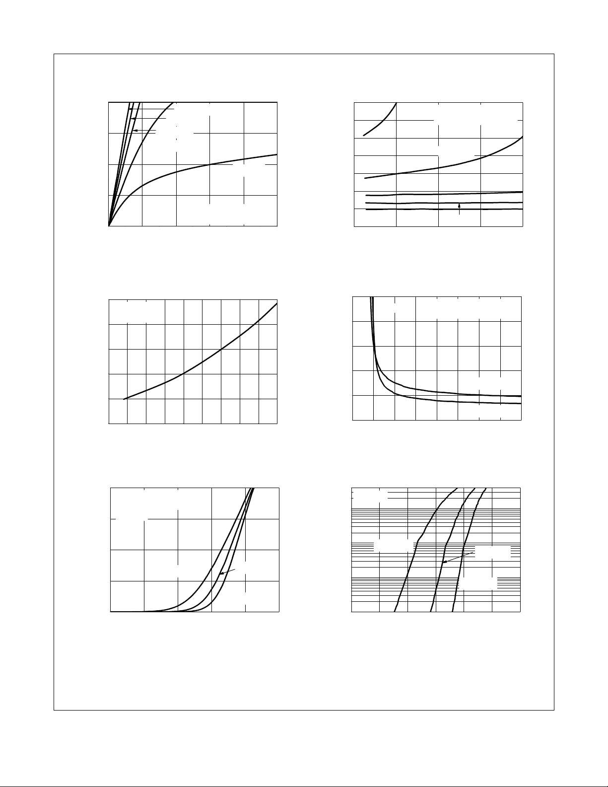
Typical Characteristics (Q1 N-Channel) T
Figure 1.
On Region Characteristics Figure 2.
= 25 °C unless otherwise noted
J
Normali z e d O n - R e s i stance
vs Drain Current and Gate Voltage
®
Power Clip
Fig u r e 3. Nor m a lized On R esistan c e
vs Junction Temperature
©2012 Fairchild Semiconductor Corporation
FDPC8013S Rev.C1
Figure 5. Transfer Characteristics
Figure 4.
On-Resistance vs Gate to
Source Voltage
Figure 6.
Source to D rain Diode
Forward Voltage vs Source Current
4
www.fairchildsemi.com
Page 5

FDPC8013S PowerTrench
03691215
0
2
4
6
8
10
ID = 13 A
V
DD
= 15 V
V
DD
= 10 V
V
GS
, GATE TO SOURCE VOLTAGE (V)
Qg, GATE CHARGE (nC)
VDD = 20 V
0.1 1 10 30
10
100
1000
2000
f = 1 MHz
V
GS
= 0 V
CAPACITANCE (pF)
VDS, DRAIN TO SOURCE VOLTAGE (V)
C
rss
C
oss
C
iss
0.001 0.01 0.1 1 10 50
1
10
50
TJ = 100 oC
TJ = 25 oC
TJ = 125 oC
tAV, TIME IN AVALANCHE (ms)
I
AS
, AVALANCHE CURRENT (A)
25 50 75 100 125 150
0
10
20
30
40
50
60
R
θJC
= 5.0 oC/W
V
GS
= 4.5 V
Limited by Package
V
GS
= 10 V
I
D
, DRAIN CURRENT (A)
T
C
, CASE TEMPERATURE (
o
C)
0.01 0.1 1 10 100
0.01
0.1
1
10
100
100 μs
DC
100 ms
10 ms
1 ms
1s
I
D
, DRAIN CURRENT (A)
VDS, DRAIN to SOURCE VOLTAGE (V)
THIS AR E A IS
LIMITED BY r
DS(on)
SINGLE PULSE
T
J
= MAX RATED
R
θJA
= 151
o
C/W
T
A
= 25
o
C
10s
10-410-310-210-110010
1
100 1000
0.5
1
10
100
1000
SINGLE PULSE
R
θJA
= 151 oC/W
P(
PK
), PEAK TRANSIENT POWER (W)
t, PULSE WIDTH (sec)
Typical Characteristics (Q1 N-Channel) T
Figure 7.
Gate Charge Characteristics Figure 8.
= 25 °C unless otherwise noted
J
Capa c i t a nce v s D r ain
to Source Voltage
®
Power Clip
Figure 9.
Unclamped Inductive
Switching Capability
©2012 Fairchild Semiconductor Corporation
FDPC8013S Rev.C1
Figure 11.
Forward Bias Safe
Operating Area
Figure 10. Maximum Continuous Drain
Current vs. Ambient Temperature
Figure 12.
Single Pu l s e M a x imum
Power Dissipation
5
www.fairchildsemi.com
Page 6

FDPC8013S PowerTrench
10
-4
10
-3
10
-2
10
-1
10
0
10
1
100 1000
0.001
0.01
0.1
1
2
SINGLE PULSE
R
θJA
= 151 oC/W
(Note 1b)
DUTY CYCLE-DESCENDING ORDER
NORMALIZED THERMAL
IMPEDANCE,
Z
θJA
t, RECTANGULAR PULSE DURATION (sec)
D = 0.5
0.2
0.1
0.05
0.02
0.01
P
DM
t
1
t
2
NOTES:
DUTY FACTOR: D = t1/t
2
PEAK TJ = PDM x Z
θJA
x R
θJA
+ T
A
Typical Characteristics (Q1 N-Channel) T
Figure 13.
Junction-to-Ambient Transient Thermal Response Curve
= 25 °C unless otherwise noted
J
®
Power Clip
©2012 Fairchild Semiconductor Corporation
FDPC8013S Rev.C1
6
www.fairchildsemi.com
Page 7

FDPC8013S PowerTrench
0.0 0.2 0.4 0.6 0.8 1.0
0
20
40
60
80
100
V
GS
= 3 V
V
GS
= 3.5 V
V
GS
= 10 V
V
GS
= 6 V
V
GS
= 4.5 V
PULSE DURATION = 80 μs
DUTY CYCLE = 0.5% MAX
I
D
, DRAIN CURRENT (A)
V
DS
, DRAIN TO SOURCE VOLTAGE (V)
020406080100
0
1
2
3
4
5
6
VGS = 3 V
VGS = 4.5 V
PULSE DURA TION = 80 μs
DUTY CYCLE = 0.5% MAX
NORMALIZED
DRAIN TO SOURCE ON-RESISTA NCE
I
D
, DRAIN CURRENT (A)
V
GS
= 3.5 V
VGS = 6 V
V
GS
= 10 V
-75 -50 -25 0 25 50 75 100 125 150
0.6
0.8
1.0
1.2
1.4
1.6
ID = 26 A
V
GS
= 10 V
NORMALIZED
DRAIN TO SOURCE ON-RESISTANCE
T
J
, JUNCTION TE M P E R ATURE (
o
C)
246810
0
1
2
3
4
5
6
7
TJ = 125 oC
ID = 26 A
TJ = 25 oC
V
GS
, GATE TO SOURCE VOLTAGE (V)
r
DS(on)
,
DRAIN TO
SOURCE ON-RESISTANCE
(mΩ)
PULSE DURATION = 80 μs
DUTY CYCLE = 0.5% MAX
1.01.52.02.53.03.5
0
20
40
60
80
100
TJ = 125 oC
V
DS
= 5 V
PULSE DURATION = 80 μs
DUTY CYCLE = 0.5% MAX
TJ = -55 oC
TJ = 25 oC
I
D
, DRAIN CURRENT (A)
VGS, GATE TO SOURCE VOLTAGE (V)
0.0 0.2 0.4 0.6 0.8 1.0
0.001
0.01
0.1
1
10
100
TJ = -55 oC
TJ = 25 oC
TJ = 125 oC
V
GS
= 0 V
I
S
, REVERSE DRAIN CURRENT (A)
VSD, BODY DIODE FORWARD VOLTAGE (V)
Typical Characteristics (Q2 N-Channel) T
Figure 14. On-Region Characteristics
= 25 oC unlenss otherwise noted
J
Figure 15. Normalized on-Resistance vs Drain
Current and Gate Voltage
®
Power Clip
Figure 16. Normalized On-Resistance
vs Junction Temperature
©2012 Fairchild Semiconductor Corporation
FDPC8013S Rev.C1
Figure 18. Transfer Characteristics
Figure 17. On-Resistance vs Gate to
Source Voltage
Figure 19. Source to Drain Diode
Forward Voltage vs Source Current
7
www.fairchildsemi.com
Page 8

0 1020304050
0
2
4
6
8
10
ID = 26 A
V
DD
= 20 V
V
DD
= 10 V
V
GS
, GATE TO SOURCE VOLTAGE (V)
Qg, GATE CHARGE (nC)
VDD = 15 V
0.1 1 10 30
50
100
1000
10000
f = 1 MHz
V
GS
= 0 V
CAPACITANCE (pF)
VDS, DRAIN TO SOURCE VOLTAGE (V)
C
rss
C
oss
C
iss
0.001 0.01 0.1 1 10 100 1000
1
10
100
TJ = 100 oC
TJ = 25 oC
TJ = 125 oC
tAV, TIME IN AVALANCHE (ms)
I
AS
, AVALANCHE CURRENT (A)
25 50 75 100 125 150
0
20
40
60
80
100
120
R
θJC
= 3.5 oC/W
V
GS
= 4.5 V
Limited by Package
V
GS
= 10 V
I
D
, DRAIN CURRENT (A)
T
C
, CASE TEMPERATURE (
o
C)
0.01 0.1 1 10 100
0.01
0.1
1
10
100
200
100 μs
DC
100 ms
10 ms
1 ms
1s
I
D
, DRAIN CURRENT (A)
VDS, DRAIN to SOURCE VOLTAGE (V)
THIS AREA IS
LIMITED BY r
DS(on)
SINGLE PULSE
T
J
= MAX RATED
R
θJA
= 135
o
C/W
T
A
= 25
o
C
10s
10-410-310-210-110010
1
100 1000
0.5
1
10
100
1000
3000
SINGLE PULSE
R
θJA
= 135 oC/W
P(
PK
), PEAK TRANSIENT POWER (W)
t, PULSE WIDTH (sec)
FDPC8013S PowerTrench
Typical Characteristics (Q2 N-Channel) T
Figure 20. Gate Charge Characteristics
= 25 oC unlenss otherwise noted
J
Figure 21. Capacitance vs Drain
to Source Voltage
®
Power Clip
Figure 22. Unclamped Inductive
itching Capability
Sw
©2012 Fairchild Semiconductor Corporation
FDPC8013S Rev.C1
Figure 24. Forward Bias Safe
Operating Area
Figure 23. Maximum Continouns Drain
Current vs Ambient Temperature
Figure 25. Single Pulse Maximum
Power Dissipation
8
www.fairchildsemi.com
Page 9

FDPC8013S PowerTrench
10
-4
10
-3
10
-2
10
-1
10
0
10
1
100 1000
1E-4
1E-3
0.01
0.1
1
2
SINGLE PULSE
R
θJA
= 135 oC/W
(Note 1b)
DUTY CYCLE-DESCENDING ORDER
NORMALIZED THERMAL
IMPEDANCE, Z
θJA
t, RECTANGULAR PULSE DURATION (sec)
D = 0.5
0.2
0.1
0.05
0.02
0.01
P
DM
t
1
t
2
NOTES:
DUTY FACTOR: D = t1/t
2
PEAK TJ = PDM x Z
θJA
x R
θJA
+ T
A
Typical Characteristics (Q2 N-Channel) T
= 25 oC unlenss otherwise noted
J
Figure 26. Junction-to-Ambient Transient Thermal Response Curve
®
Power Clip
©2012 Fairchild Semiconductor Corporation
FDPC8013S Rev.C1
9
www.fairchildsemi.com
Page 10

100 150 200 250 300 350 400
-5
0
5
10
15
20
25
30
CURRENT (A)
TIME (ns)
di/dt = 300 A/μs
0 5 10 15 20 25 30
1
10
10
2
10
3
10
4
TJ = 125 oC
TJ = 100 oC
TJ = 25 oC
I
DSS
, REVERSE LEAKAGE CURRENT (uA)
VDS, REVERSE VOLTAGE (V)
Typical Characteristics (continued)
SyncFETTM Schottky body diode
Characteristics
FDPC8013S PowerTrench
Fairchild’s SyncFETTM process embeds a Schottky diode in
parallel with PowerTrench MOSFET. This diode exhibits similar
characteristics to a discrete external Schottky diode in parallel
with a MOSFET. Figure 27 shows the reverse recovery
characteristic of the FDPC8013S.
Figure 27. FDPC8013S SyncFET
TM
body
diode reverse recovery characteristic
Schottky barrier diodes exhibit significant leakage at high temperature and high reverse voltage. This will increase the power
in the device.
Figure 28. SyncFET
TM
body diode reverse
leakage versus drain-source voltage
®
Power Clip
©2012 Fairchild Semiconductor Corporation
FDPC8013S Rev.C1
10
www.fairchildsemi.com
Page 11

Dimensional Outline and Pad Layout
FDPC8013S PowerTrench
®
Power Clip
©2012 Fairchild Semiconductor Corporation
FDPC8013S Rev.C1
11
www.fairchildsemi.com
Page 12

TRADEMARKS
®
™
tm
tm
The following includes registered and unregistered trademarks a nd service marks, owned by Fairch ild Semiconductor and/ or its global subsidiaries, and is n ot
intended to be an exhaustive list of all such trademarks.
2Cool™
AccuPower™
AX-CAP™*
®
BitSiC
Build it Now™
CorePLUS™
CorePOWER™
CROSSVOLT™
CTL™
Current Transfer Logic™
DEUXPEED
Dual Cool™
EcoSPARK
EfficentMax™
®
®
ESBC™
®
Fairchild
Fairchild Semiconductor
FACT Quiet Series™
®
FACT
®
FAST
FastvCore™
FETBench™
FlashWriter
®
*
FPS™
®
F-PFS™
®
FRFET
Global Power Resource
Green Bridge™
Green FPS™
Green FPS™ e-Series™
Gmax™
GTO™
IntelliMAX™
ISOPLANAR™
Marking Small Speakers Sound Louder
and Better™
MegaBuck™
MICROCOUPLER™
MicroFET™
MicroPak™
MicroPak2™
MillerDrive™
MotionMax™
Motion-SPM™
mWSaver™
OptoHiT™
OPTOLOGIC
OPTOPLANAR
®
®
®
SM
PowerTrench
PowerXS™
Programmable Active Droop™
QFET
QS™
Quiet Series™
RapidConfigure™
Saving our world, 1mW/W/kW at a time™
SignalWise™
SmartMax™
SMART START™
Solutions for Your Success™
SPM
STEALTH™
SuperFET
SuperSOT™-3
SuperSOT™-6
SuperSOT™-8
SupreMOS
SyncFET™
Sync-Lock™
®
®
®
®
®
®*
The Power Franchise
TinyBoost™
TinyBuck™
TinyCalc™
TinyLogic
TINYOPTO™
TinyPower™
TinyPWM™
TinyWire™
TranSiC
TriFault Detect™
TRUECURRENT
μSerDes™
UHC
Ultra FRFET™
UniFET™
VCX™
VisualMax™
VoltagePlus™
®
®
®
®
XS™
®
®
*
*Trademarks of System General Corporation, used under license by Fairchild Semiconductor.
DISCLAIMER
FAIRCHILD SEMICONDUCTOR RESERVES THE RIGHT TO MAKE CHANGES WITHOUT FURTHER NOTICE TO ANY PRODUCTS HEREIN TO IMPROVE
RELIABILITY, FUNCTION, OR DESIGN. FAIRCHILD DOES NOT ASSUME ANY LIABILITY ARISING OUT OF THE APPLICATION OR USE OF ANY
PRODUCT OR CIRCUIT DESCRIBED HEREIN; NEITHER DOES IT CONVEY ANY LICENSE UNDER ITS PATENT RIGHTS, NOR THE RIGHTS OF OTHERS.
THESE SPECIFICATIONS DO NOT EXPAND THE TERMS OF FAIRCHILD’S WORLDWIDE TERMS AND CONDITIONS, SPECIFICALLY THE WARRANTY
THEREIN, WHICH COVERS THESE PRODUCTS.
FDPC8013S PowerTrench
®
Power Clip
LIFE SUPPORT POLICY
FAIRCHILD’S PRODUCTS ARE NOT AUTHORIZED FOR USE AS CRITICAL COMPONENTS IN LIFE SUPPORT DEVICES OR SYSTEMS WITHOUT THE
EXPRESS WRITTEN APPROVAL OF FAIRCHILD SEMICONDUCTOR CORPORATION.
As used here in:
1. Life support devices or systems are devices or systems which, (a) are
intended for surgical implant into the bo dy or (b ) support or su stain life,
and (c) whose failure to perform when properly used in accordan ce with
instructions for use provided in the labeling, can be reasonably
2. A critical component in any component of a life support, device, or
system whose failure to perform can be reasonably expected to cause
the failure of the life support device or system, or to affect its safety or
effectiveness.
expected to result in a significant injury of the user.
ANTI-COUNTERFEITING POLICY
Fairchild Semiconductor Corporation’s Anti-Counterfeiting Policy. Fairchild’s Anti-Counterfeiting Policy is also stated on our external website,
www.Fairchildsemi.com, under Sales Support
Counterfeiting of semiconductor parts is a growing problem in the industry. All manufactures of semiconductor products are exper iencing counterfeiting of their
parts. Customers who inadvertently purchase counterfeit part s expe rience many problems such as loss of brand repu tation, substa ndar d pe rformance, fail ed
application, and increased cost of production and manufacturing delays. Fairchild is taki ng st ron g measures to prote ct ourselves and our custo mers from the
proliferation of counterfeit parts. Fairchild strongl y encourages customers t o purchase Fairchil d parts either d irectly from Fairchild o r from Authorized Fairchi ld
Distributors who are listed by country on our web page cited above. Products customers buy either from Fairchild directly or from Authorized Fairchild
Distributors are genuine parts, have full traceability, meet Fairchild’s quality standards for handing and storage and provide access to Fairchild’s full range of
up-to-date technical and product information. Fairchild and our Authorized Distributors will stand behind all warranties and will appropriately address and
warranty issues that may arise. Fairchild will not provide any warranty coverage or other assistance for parts bought from Unauthorized Sources. Fairchild is
committed to combat this global problem and encourage our customers to do their part in stopping this practi ce by buying direct or fr om authorized distributors.
PRODUCT STATUS DEFINITIONS
Definition of Terms
.
Datasheet Identification Product Status Definition
Advance Information Formative / In Design
Preliminary First Production
No Identification Needed Full Production
Obsolete Not In Production
Datasheet contains the design specifications for product development. Specifications
may change in any manner without notice.
Datasheet contains preliminary data; supplementa ry data will be published at a later
date. Fairchild Semiconductor reserves the right to make changes at any time without
notice to improve design.
Datasheet contains final specifications. Fairchild Semiconductor reserves the right to
make changes at any time without notice to improve the design.
Datasheet contains specifications on a product that is discontinued by Fairchild
Semiconductor. The datasheet is for reference information only.
Rev. I61
©2012 Fairchild Semiconductor Corporation
FDPC8013S Rev.C1
12
www.fairchildsemi.com
 Loading...