

Page 1
FDP8876
N-Channel PowerTrench® MOSFET
30V, 71A, 8.5mΩ
FDP8876 N-Channel PowerTrench
November 2005
General Descriptions
This N-Channel MOSFET has been designed specifically to
improve the overall efficiency of DC/DC converters using
either synchronous or conventional switching PWM
controllers. It has been optimized for low gate charge, low
r
and fast switching speed.
DS(ON)
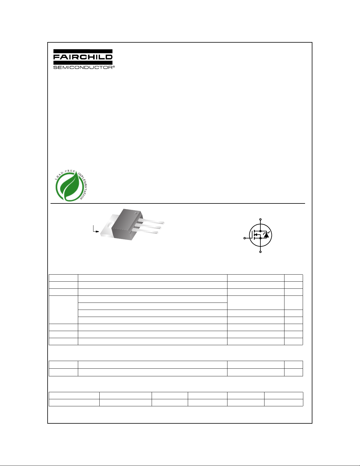
DRAIN
(FLANGE)
TO-220AB
FDP SERIES
MOSFET Maximum Ratings T
Symbol Parameter Ratings Units
V
DSS
V
GS
I
D
E
AS
P
D
, T
T
J
STG
Drain to Source Voltage 30 V
Gate to Source Voltage ±20 V
Drain Current
Continuous (T
Continuous (T
Pulsed Figure 4 A
Single Pulse Avalanche Energy (Note 1) 180 mJ
Power dissipation 70 W
Operating and Storage Temperature -55 to 175
= 25oC, VGS = 10V)
C
= 25oC, VGS = 4.5V) 64 A
C
A
SOURCE
DRAIN
GATE
= 25°C unless otherwise noted
Features
r
r
High performance trench technology for extremely low
Low gate charge
High power and current handling capability
RoHS Compliant
DS(ON)
DS(ON)
r
DS(ON)
= 8.5mΩ, V
= 10.3mΩ, V
= 10V, ID = 40A
GS
= 4.5V, ID = 40A
GS
G
D
S
70 A
®
MOSFET
o
C
Thermal Characteristics
R
θJC
R
θJA
Thermal Resistance Junction to Case TO-263 2.14
Thermal Resistance Junction to Ambient TO-263,1in2copper pad area 62
Package Marking and Ordering Information
Device Marking Device Package Reel Size Tape Width Quantity
FDP8876 FDP8876 TO-220AB Tube N/A 50 units
©2005 Fairchild Semiconductor Corporation
FDP8876 Rev. A
o
C/W
o
C/W
www.fairchildsemi.com1
Page 2
FDP8876 N-Channel PowerTrench
Electrical Characteristics T
= 25°C unless otherwise noted
A
Symbol Parameter Test Conditions Min Typ Max Units
Off Characteristics
B
I
DSS
I
GSS
VDSS
Drain to Source Breakdown Voltage ID = 250µA, VGS = 0V 30 - - V
Zero Gate Voltage Drain Current
VDS = 24V 1 µA
VGS = 0V TA = 150oC - - 250
Gate to Source Leakage Current VGS = ±20V - - ±100 nA
On Characteristics
V
GS(TH)
r
DS(ON)
Gate to Source Threshold Voltage VGS = VDS, ID = 250µA 1.2 - 2.5 V
ID = 40A, VGS = 10V - 6.1 8.7
Drain to Source On Resistance
ID = 40A, VGS = 4.5V - 7.7 10.5
ID = 40, VGS = 10V,
TA = 175oC
- 11 14
Dynamic Characteristics
C
ISS
C
OSS
C
RSS
R
G
Q
g(TOT)
Q
g(5)
Q
g(TH)
Q
gs
Q
gs2
Q
gd
Input Capacitance
Output Capacitance - 340 - pF
Reverse Transfer Capacitance - 210 - pF
VDS = 15V, VGS = 0V,
f = 1MHz
- 1700 - pF
Gate Resistance VGS=0.5V, f = 1MHz - 2.3 - Ω
Total Gate Charge at 10V VGS = 0V to 10V
Total Gate Charge at 5V VGS = 0V to 5V - 17 24 nC
Threshold Gate Charge VGS = 0V to 1V - 1.6 2.4 nC
VDD = 15V
ID = 40A
Ig = 1.0mA
- 32 45 nC
Gate to Sourse Gate Charge - 4.7 - nC
Gate Charge Threshold to Plateau - 3.1 - nC
Gate to Drain “Miller” Charge - 7.0 - nC
mΩ
®
MOSFET
Switching Characteristics (V
t
ON
t
d(ON)
t
r
t
d(OFF)
t
f
t
OFF
Turn-On Time
Turn-On Delay Time - 9 - ns
Rise Time - 97 - ns
Turn-Off Delay Time - 51 - ns
Fall Time - 39 - ns
Turn-Off Time - - 135 ns
GS
= 10V)
Drain-Source Diode Characteristic
V
SD
t
rr
Q
RR
Notes:
1: Starting TJ=25OC,L=1mH,IAS=19A,VDD=27V,VGS=10V
2: Pulse width=100s
Source to Drain Diode Voltage
Reverse Recovery Time ISD = 40A, dISD/dt=100A/µs - - 22 ns
Reverse Recovered Charge ISD = 40A, dISD/dt=100A/µs - - 9 nC
- - 189 ns
VDD = 15V, ID = 40A
VGS = 10V, RGS = 10Ω
I
= 40A - - 1.25 V
SD
ISD = 3.2A - - 1.0 V
FDP8876 Rev. A
www.fairchildsemi.com2
Page 3

FDP8876 N-Channel PowerTrench
Typical Characteristics T
= 25°C unless otherwise noted
A
100
VGS=10V
80
60
VGS=4.5V
VGS=3.5V
40
,DRAIN DURRENT(A)
D
I
20
PULSE DURATION=80µS
0
0.0 0.5 1.0 1.5 2.0 2.5
VDS,DRAIN TO SOURSE VOLTAGE(V)
DUTY CYCLE=0.5 %MAX
Figure 1. On Region Characteristics
1.6
ID = 40A
VGS = 10V
1.4
1.2
, NORMALIZED
1.0
DS(ON)
R
0.8
DRAIN-SOURCE ON-RESISTANCE
0.6
-80 -40 0 40 80 120 160 200
PULSE DURATION=80µ S
DUTY CYCLE=0.5%MAX
TJ, JUNCTION TEMPERATURE (oC)
VGS=3V
TC=25oC
2.6
2.4
PULSE DURATION = 80µs
DUTY CYCLE = 0.5% MAX
2.2
2.0
1.8
1.6
, NORMALIZED
1.4
1.2
DS(ON)
R
1.0
0.8
DRAIN TO SOURCE ON-RESISTANCE
0.6
10 20 30 40 50 60 70 80
ID,DRAIN CURRENT
Figure 2.
On-Resistance Variation with Drain
Current and Gate Voltage
, ON-RESISTANCE (OHM)
R
DS(ON)
0.016
0.014
0.012
0.010
0.008
0.006
PULSE DURATION=80µS
DUTY CYCLE=0.5%MAX
TA = 125oC
TA = 25oC
345678910
VGS, GATE TO SOURCE VOLTAGE (V)
3v
3.5v
4v
4.5v
5v
10v
®
MOSFET
ID=40A
Figure 3.
160
PULSE DURATION = 80ms
DUTY CYCLE = 0.5% MAX
V
120
80
, DRAIN CURRENT (A)
D
40
I
0
1.5 2.0 2.5 3.0 3.5 4.0 4.5
Figure 5. Transfer Characteristics
FDP8876 Rev. A
On Resistance Variation with
Temperature
= 15V
DD
TJ = 175oC
TJ = 25oC
VGS, GATE TO SOURCE VOLTAGE (V)
TJ = -55oC
Figure 4.
On-Resistance Variation with
Gate-to-Source Votlage
100
VGS=0V
10
125oC
1
25oC
0.1
, REVERSE DRAIN CURRENT (A)
S
I
0.01
0.00.20.40.60.81.01.21.4
Figure 6.
VSD, BODY DIODE FORWARD VOLTAGE (V)
Body Diode Forward Voltage Variation
-25oC
With Source Current and Temperature
www.fairchildsemi.com3
Page 4

Typical Characteristics T
= 25°C unless otherwise noted
A
FDP8876 N-Channel PowerTrench
10
VDD=15V
8
6
4
,GATE TO SOURCE VOLTAGE(V)
2
GS
V
0
0 5 10 15 20 25 30 35
Figure 7.
100
10
STARTING TJ = 150oC
, AVALANCHE CURRENT (A)
If R = 0
AS
I
tAV = (L)(IAS)/(1.3*RATED BV
≠
0
If R
= (L/R)ln[(IAS*R)/(1.3*RATED BV
t
AV
1
0.001 0.01 0.1 1 10 100
Qg,GATE CHARGE(nC)
Gate Charge characteristics Figure 8.
tAV, TIME IN AVALANCHE (ms)
WAVEFORMS IN
DESCENDING ORDER:
=40A,ID=5A
I
D
STARTING TJ = 25oC
- VDD)
DSS
- VDD) +1]
DSS
Figure 9. Unclamped Inductive Switching
Capability
5000
1000
C
=
C
RSS
V
= 0V, f = 1MHz
GS
GD
C, CAPACITANCE (pF)
100
0.1 1 10
VDS, DRAIN TO SOURCE VOLTAGE (V)
Saturation characteristics
1000
100
10
OPERATION IN THIS
AREA MAY BE
D
1
0.1
LIMITED BY r
SINGLE PULSE
TJ = MAX RATED
T
= 25oC
C
1
Figure 10.
DS(ON)
VDS, DRAIN TO SOURCE VOLTAGE (V)
10
Safe Operating Area
, DRAIN CURRENT (A)
I
C
=
CGS + C
ISS
C
OSS
GD
≅
C
+ C
DS
GD
30
®
MOSFET
10µs
100µs
1ms
10ms
DC
60
80
60
40
20
, DRAIN CURRENT (A)
D
I
0
25 50 75 100 125 150 175
VGS = 10V
VGS = 4.5V
TC, CASE TEMPERATURE (oC)
Figure 11. Maximum Continuous Drain Current vs
Case Temperature
FDP8876 Rev. A
, PEAK TRANSIENT POWER (W)
P
800
100
(PK)
60
-5
10
-4
10
-3
10
-2
10
t, PULSE WIDTH (s)
SINGLE PULSE
R
θ
JC
= 25oC
T
J
-1
10
= 2.14oC/W
0
10
10
Figure 12. Normalized Drain to Source Breake
Down Voltage vs Junction Temperature
www.fairchildsemi.com4
1
Page 5

Typical Characteristics T
2
DUTY CYCLE - DESCENDING ORDER
0.5
1
0.2
0.1
0.05
0.02
0.01
0.1
, NORMALIZED
θJC
Z
THERMAL IMPEDANCE
SINGLE PULSE
0.01
-5
10
-4
10
= 25°C unless otherwise noted
A
-3
10
t, RECTANGULAR PULSE DURATION (s)
-2
10
NOTES:
DUTY FACTOR: D = t
PEAK TJ = PDM x Z
-1
10
qJC
FDP8876 N-Channel PowerTrench
P
DM
t
1
t
2
1/t2
x R
+ T
qJC
C
0
10
1
10
Figure 13.
Normolized Maximum Transient Thermal Impedance
®
MOSFET
FDP8876 Rev. A
www.fairchildsemi.com5
Page 6

TRADEMARKS
The following are registered and unregistered trademarks Fairchild Semiconductor owns or is authorized to use and is
not intended to be an exhaustive list of all such trademarks.
ACEx™
ActiveArray™
Bottomless™
FPS™
Build it Now™
CoolFET™
CROSSVOLT™
DOME™
EcoSPARK™
2
E
CMOS™
EnSigna™
FACT™
FACT Quiet Series™
Across the board. Around the world.™
The Power Franchise
Programmable Active Droop™
DISCLAIMER
FAIRCHILD SEMICONDUCTOR RESERVES THE RIGHT TO MAKE CHANGES WITHOUT FURTHER NOTICE T O ANY
PRODUCTS HEREIN TO IMPROVE RELIABILITY , FUNCTION OR DESIGN. FAIRCHILD DOES NOT ASSUME ANY LIABILITY
ARISING OUT OF THE APPLICATION OR USE OF ANY PRODUCT OR CIRCUIT DESCRIBED HEREIN; NEITHER DOES IT
CONVEY ANY LICENSE UNDER ITS PA TENT RIGHTS, NOR THE RIGHTS OF OTHERS.
LIFE SUPPORT POLICY
®
FAST
FAST r™
LittleFET™
FRFET™
GlobalOptoisolator™
GTO™
HiSeC™
2
I
C™
i-Lo™
ImpliedDisconnect™
IntelliMAX™
®
ISOPLANAR™
MICROCOUPLER™
MicroFET™
MicroPak™
MICROWIRE™
MSX™
MSXPro™
OCX™
OCXPro™
OPTOLOGIC
®
OPTOPLANAR™
PACMAN™
POP™
Power247™
PowerEdge™
PowerSaver™
PowerTrench
®
QFET
®
QS™
QT Optoelectronics™
Quiet Series™
RapidConfigure™
RapidConnect™
μSerDes™
ScalarPump™
SILENT SWITCHER
SMART ST ART™
SPM™
Stealth™
SuperFET™
SuperSOT™-3
SuperSOT™-6
SuperSOT™-8
SyncFET™
TinyLogic
TINYOPTO™
TruTranslation™
UHC™
UltraFET
UniFET™
VCX™
®
Wire™
®
®
FAIRCHILD’S PRODUCTS ARE NOT AUTHORIZED FOR USE AS CRITICAL COMPONENTS IN LIFE SUPPORT
DEVICES OR SYSTEMS WITHOUT THE EXPRESS WRITTEN APPROVAL OF FAIRCHILD SEMICONDUCTOR CORPORA TION.
As used herein:
1. Life support devices or systems are devices or
systems which, (a) are intended for surgical implant into
the body, or (b) support or sustain life, or (c) whose
failure to perform when properly used in accordance
with instructions for use provided in the labeling, can be
reasonably expected to result in significant injury to the
user.
PRODUCT STA TUS DEFINITIONS
Definition of Terms
Datasheet Identification Product Status Definition
Advance Information
Preliminary
No Identification Needed
Formative or
In Design
First Production
Full Production
2. A critical component is any component of a life
support device or system whose failure to perform can
be reasonably expected to cause the failure of the life
support device or system, or to affect its safety or
effectiveness.
This datasheet contains the design specifications for
product development. Specifications may change in
any manner without notice.
This datasheet contains preliminary data, and
supplementary data will be published at a later date.
Fairchild Semiconductor reserves the right to make
changes at any time without notice in order to improve
design.
This datasheet contains final specifications. Fairchild
Semiconductor reserves the right to make changes at
any time without notice in order to improve design.
Obsolete
Not In Production
This datasheet contains specifications on a product
that has been discontinued by Fairchild semiconductor.
The datasheet is printed for reference information only.
Rev. I17
 Loading...