

Page 1
tm
FDP5800
N-Channel Logic Level PowerTrench
60V,80A, 6mΩ
®
MOSFET
FDP5800 N-Channel Logic Level PowerTrench
November 2006
Features
•R
• High performance trench technology for extermly low Rdson
• Low gate Charge
• High power and current handing capability
•RoHs Compliant
= 4.6mΩ (Typ.), VGS = 10V, ID = 80A
DS(on)
Applications
• Motor/ Body Load Control
• Power Train Management
• Injection Systems
• DC-AC Converters and UPS
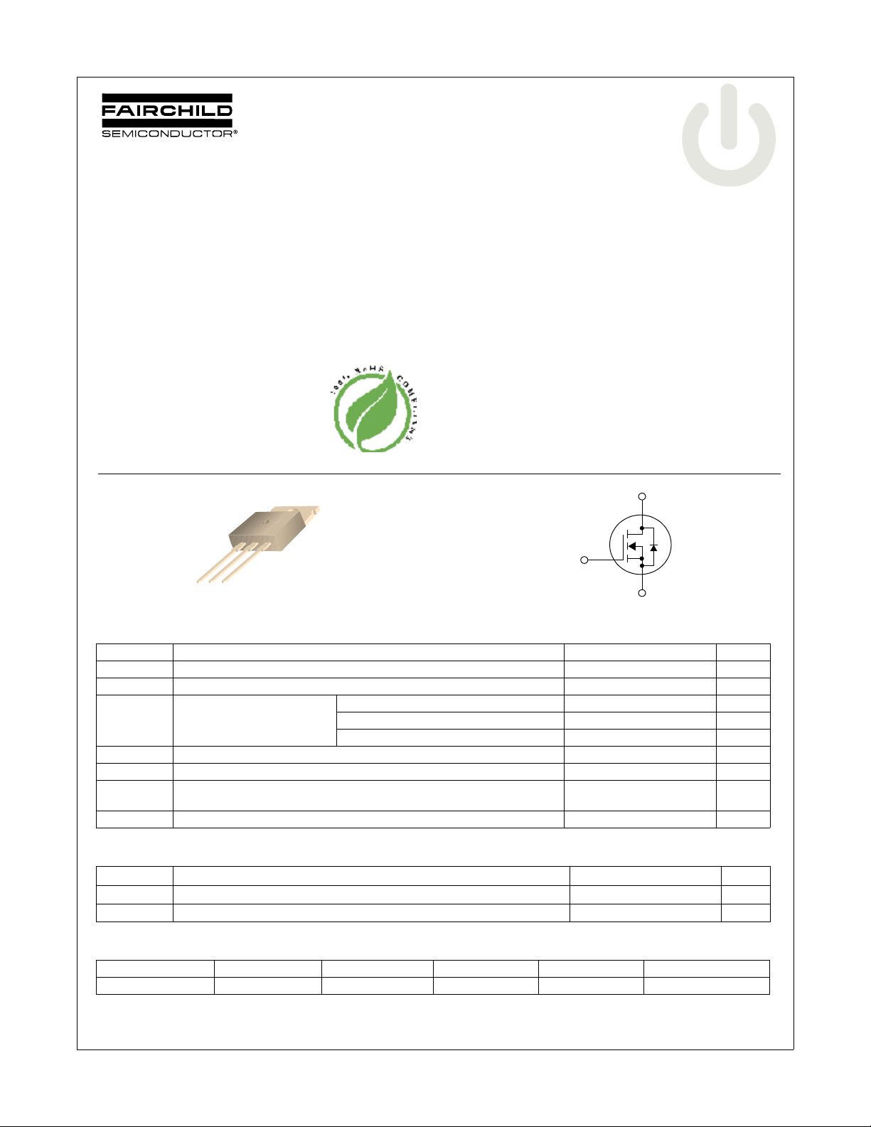
G
D
TO-220
S
D
G
MOSFET Maximum Ratings T
Symbol Parameter Ratings Units
V
DSS
V
GSS
I
D
I
DM
E
AS
P
D
, T
T
J
STG
*Drain current limited by package
Drain-Source Voltage 60 V
Gate-Source Voltage ±20 V
D r a i n C u r r e n t
Drain Current - Pulsed 320 A
Single Pulsed Avalanche Energy (Note 1) 652 mJ
Power Dissipation (TC = 25oC)
- Derate above 25
Operating and Storage Temperature Range -55 to +175 °C
FDP Series
= 25°C unless otherwise noted*
C
-Continuous (T
-Continuous (T
-Continuous (T
= 25oC) 80 A
C
= 100oC) A 80*
C
= 25oC) 14 A
A
o
C
S
242
1.61
Thermal Characteristics
R
θJC
R
θJA
R
θJA
Thermal Resistance , Junction to Case 0.62 °C/W
Thermal Resistance , Junction to Ambient, 1in2 copper pad area 43 °C/W
Thermal Resistance , Junction to Ambient 62.5 °C/W
®
MOSFET
W
W/°C
Package Marking and Ordering Information
Device Marking Device Package Reel Size Tape Width Quantity
FDP5800 FDP5800 TO220 -- -- 50
©2006 Fairchild Semiconductor Corporation
FDP5800 Rev. A
www.fairchildsemi.com1
Page 2
FDP5800 N-Channel Logic Level PowerTrench
Electrical Characteristics T
= 25°C unless otherwise noted
C
Symbol Parameter Conditions Min Typ Max Units
Off Characteristics
B
I
DSS
I
GSS
VDSS
Drain-Source Breakdown Voltage ID = 250µA, VGS = 0V, TJ =25oC60 -- --V
V
= 48V
Zero Gate Voltage Drain Current
DS
V
= 0V
GS
Gate-Body Leakage Current, Forward VGS = ±20V, V
= 150°C -- -- 500 µA
T
J
= 0V -- -- ±100 nA
DS
-- -- 1 µA
On Characteristics
V
GS(th)
R
DS(on)
Gate Threshold Voltage VGS = VDS, ID = 250µA1.0--2.5V
= 10V , ID = 80A -- 4.6 6.0 mΩ
V
GS
=4.5V , ID = 80A -- 5.9 7.2 mΩ
V
Static Drain-Source On Resistance
GS
= 5V , ID = 80A -- 5.6 7.0 mΩ
V
GS
=10V, ID = 80A
V
GS
T
= 175oC
J
-- 10.4 12.6 mΩ
Dynamic Characteristics
C
iss
C
oss
C
rss
R
G
Q
g(TOT)
Q
g(TH)
Q
g(TH)
Q
gs
Q
gs2
Q
gd
Input Capacitance
Output Capacitance -- 750 1000 pF
Reverse Transfer Capacitance -- 295 445 pF
= 15V,VGS = 0V
V
DS
f = 1MHz
Gate Resistance VGS = 0.5V, f = 1MHz -- 1.2 -- Ω
Total Gate Charge at 10V VGS = 0V to 10V
Total Gate Charge at 5V VGS = 0V to 5V -- 58 -- nC
Threshold Gate Charge VGS = 0V to 1V -- 7.0 -- nC
Gate to Source Gate Charge -- 23 -- nC
Gate Charge Threshold to Plateau -- 13 -- nC
V
DS
I
D
I
g
= 30V
= 80A
= 1mA
Gate to Drain “Miller” Charge -- 18 -- nC
-- 6890 9160 pF
-- 112 145 nC
®
MOSFET
Switching Characteristics
t
ON
t
d(on)
t
r
t
d(off)
t
f
t
OFF
Turn-On Time
Turn-On Delay Time -- 18 46 ns
Turn-On Rise Time -- 19 47 ns
Turn-Off Delay Time -- 55 120 ns
Turn-Off Fall Time -- 9 28 ns
Turn-Off Time -- 64 138 ns
(VGS = 10V)
Drain-Source Diode Characteristics
V
SD
t
rr
Q
rr
Notes:
1: L = 1mH, IAS = 36A, VDD = 54V, VGS = 10V, RG = 25Ω, Starting TJ = 25oC
Drain-Source Diode Forward Voltage
Reverse Recovery Time
Reverse Recovery Charge -- 106 -- nC
= 30V, ID = 80A
V
DD
V
= 10V, R
GS
V
= 0V, I
GS
= 0V, I
V
GS
V
= 0V, I
GS
dI
/dt = 100A/µs
F
-- 37 85 ns
= 1.5Ω
GEN
= 80A -- -- 1.25 V
SD
= 40A -- -- 1.0 V
SD
SD
= 60A
-- 58 -- ns
FDP5800 Rev. A
2
www.fairchildsemi.com
Page 3
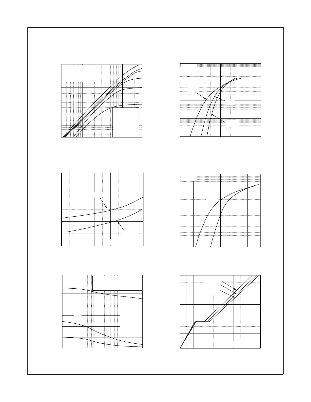
Typical Performance Characteristics
FDP5800 N-Channel Logic Level PowerTrench
Figure 1. On-Region Characteristics Figure 2. Transfer Characteristics
400
* Notes :
µs Pulse Test
1. 250
= 25oC
2. T
C
100
,Drain Current[A]
D
I
10
5
0.03
0.1 1
VDS,Drain-Source Voltage[V]
V
Top : 10.0 V
5.0 V
4.5 V
4.0 V
3.5 V
Bottom : 3.0 V
GS
1000
VDS = 6V
100
150oC
10
3
,Drain Current[A]
D
I
1
0.1
12345
VGS,Gate-Source Voltage[V]
25oC
-55oC
Figure 3. On-Resistance Variation vs. Figure 4. Body Diode Forward Voltage
Drain Current and Gate Voltage Variation vs. Source Current
and Temperatue
5.5
5.0
VGS = 10V
1000
100
VGS = 0V
150oC
®
MOSFET
[mΩ],
DS(ON)
4.5
R
Drain-Source On-Resistance
4.0
0 40 80 120 160 200
* Note : TJ = 25oC
ID, Drain Current [A]
VGS = 20V
10
, Reverse Drain Current [A]
S
I
1
0.2 0.4 0.6 0.8 1.0 1.2 1.4
VSD, Body Diode Forward Voltage [V]
25oC
Figure 5. Capacitance Characteristics Figure 6. Gate Charge Characteristics
10000
9000
7500
6000
4500
3000
Capacitances [pF]
1500
100
C
= Cgs + Cgd (Cds = shorted)
iss
C
= Cds + C
C
iss
oss
C
rss
= C
gd
gd
C
oss
C
rss
-1
10
0
10
VDS, Drain-Source Voltage [V]
* Note:
1. V
= 0V
GS
2. f = 1MHz
1
10
30
10
8
VDS = 25V
V
= 35V
DS
= 50V
V
DS
6
4
, Gate-Source Voltage [V]
GS
V
2
0
0 20406080100120
* Note : ID = 80A
Qg, Total Gate Charge [nC]
FDP5800 Rev. A
3
www.fairchildsemi.com
Page 4

Typical Performance Characteristics (Continued)
Figure 7. Breakdown Voltage Variation Figure 8. On-Resistance Variation
vs. Temperature vs. Temperature
1.2
2.4
FDP5800 N-Channel Logic Level PowerTrench
1.1
2.0
1.6
1.0
, [Normalized]
DSS
BV
0.9
Drain-Source Breakdown Voltage
0.8
-100 -50 0 50 100 150 200
TJ, Junction Temperature [oC]
* Notes :
1. V
GS
2. I
= 250µA
D
= 0V
, [Normalized]
1.2
DS(on)
r
0.8
Drain-Source On-Resistance
0.4
-80 -40 0 40 80 120 160 200
TJ, Junction Temperature [oC]
Figure 9. Maximum Safe Operating Area Figure 10. Maximum Drain Current
vs. Case Temperature
3
10
2
10
Operation in This Area
, Drain Current [A]
1
D
is Limited by R
I
10
0
10
0
10
DS(on)
* Notes :
= 25oC
1. T
C
2. T
= 175oC
J
3. Single Pulse
1
VDS, Drain-Source Voltage [V]
10
20µs
100µs
1ms
10ms
DC
10
2
125
CURRENT LIMITED
100
BY PACKAGE
75
50
, Drain Current [A]
D
I
25
0
25 50 75 100 125 150 175
TC, Case Temperature [oC]
Figure 11. Transient Thermal Response Curve
1
D = 0.5
* Notes :
1. V
GS
2. I
= 80A
D
= 10V
®
MOSFET
FDP5800 Rev. A
(t),Thermal Response
θJC
Z
0.1
0.01
1E-3
10
0.2
0.1
0.05
0.02
0.01
-5
Single pulse
-4
10
* Notes :
1. Z
2. Duty Factor, D=t
3. TJM - TC = PDM * Z
10
-3
10
-2
10
-1
10
t1, Square Wave Pulse Duration [sec]
4
P
DM
t
1
(t) = 0.62oC/W Max.
θJC
0
10
t
2
1/t2
(t)
θJC
1
10
2
www.fairchildsemi.com
Page 5

Gate Charge Test Circuit & Waveform
Resistive Switching Test Circuit & Waveforms
FDP5800 N-Channel Logic Level PowerTrench
Unclamped Inductive Switching Test Circuit & Waveforms
®
MOSFET
FDP5800 Rev. A
5
www.fairchildsemi.com
Page 6

Peak Diode Recovery dv/dt Test Circuit & Waveforms
g
p
g
p
+
+
V
V
DS
DS
_
_
L
LL
Sam e Type
Sam e Type
as DU T
as DU T
• dv/dt controlled by R
• dv/dt controlled by R
•ISDcontrolled by pulse period
•ISDcontrolled by pulse period
G
G
V
V
GS
GS
R
R
Driver
Driver
G
G
DUT
DUT
I
I
SD
SD
V
V
DD
DD
FDP5800 N-Channel Logic Level PowerTrench
®
MOSFET
V
V
GS
GS
( D riv e r )
( D riv e r )
I
I
SD
SD
( D U T )
( D U T )
V
V
DS
DS
( DUT )
( DUT )
G ate P ulse W idth
G ate P ulse W idth
G ate P ulse W idth
--------------------------
--------------------------
--------------------------
D =
D =
D =
Gate Pulse Period
Gate Pulse Period
Gate Pulse Period
IFM, B ody D iode Forw ard C urrent
IFM, B ody D iode Forw ard C urrent
I
I
RM
RM
Body D iode Reverse C urrent
Body D iode Reverse C urrent
Body D iode R ecovery dv/dt
Body D iode R ecovery dv/dt
V
V
SD
SD
Body Diode
Body Diode
Forw ard Volta
Forw ard Volta
e D ro
e D ro
di/dt
di/dt
10V
10V
V
V
DD
DD
FDP5800 Rev. A
6
www.fairchildsemi.com
Page 7

Mechanical Dimensions
FDP5800 N-Channel Logic Level PowerTrench
TO-220
(1.70)
9.20 ±0.2013.08 ±0.20
1.30 ±0.10
(1.46)
(1.00)
1.27 ±0.10
9.90 ±0.20
(8.70)
ø3.60 ±0.10
(3.70)(3.00)
(45°)
1.52 ±0.10
2.80 ±0.1015.90 ±0.20
18.95MAX.
4.50 ±0.20
+0.10
1.30
–0.05
®
MOSFET
FDP5800 Rev. A
2.54TYP
±0.20]
[2.54
10.00 ±0.20
0.80 ±0.10
2.54TYP
±0.20]
[2.54
10.08 ±0.30
+0.10
0.50
–0.05
7
2.40 ±0.20
www.fairchildsemi.com
Page 8

TRADEMARKS
The following are registered and unregistered trademarks Fairchild Semiconductor owns or is authorized to use and is not
intended to be an exhaustive list of all such trademarks.
ACEx™
ActiveArray™
Bottomless™
Build it Now™
CoolFET™
CROSSVOLT™
DOME™
EcoSPARK™
2
E
CMOS™
EnSigna™
®
FACT
®
FAST
FASTr™
FPS™
FRFET™
FACT Quiet Series™
GlobalOptoisolator™
GTO™
HiSeC™
2
I
C™
i-Lo™
ImpliedDisconnect™
IntelliMAX™
ISOPLANAR™
LittleFET™
MICROCOUPLER™
MicroFET™
MicroPak™
MICROWIRE™
MSX™
MSXPro™
Across the board. Around the world.™
The Power Franchise
®
OCX™
OCXPro™
OPTOLOGIC
®
OPTOPLANAR™
PACMAN™
POP™
Power247™
PowerEdge™
PowerSaver™
PowerTrench
QFET
®
®
QS™
QT Optoelectronics™
Quiet Series™
RapidConfigure™
RapidConnect™
µSerDes™
ScalarPump™
SILENT SWITCHER
SMART START™
SPM™
Stealth™
SuperFET™
SuperSOT™-3
SuperSOT™-6
SuperSOT™-8
SyncFET™
TCM™
TinyBoost™
TinyBuck™
TinyPWM™
TinyPower™
TinyLogic
®
TINYOPTO™
TruTranslation™
®
UHC
Programmable Active Droop™
DISCLAIMER
FAIRCHILD SEMICONDUCTOR RESERVES THE RIGHT TO MAKE CHANGES WITHOUT FURTHER NOTICE TO ANY PRODUCTS HEREIN TO
IMPROVE RELIABILITY, FUNCTION OR DESIGN. FAIRCHILD DOES NOT ASSUME ANY LIABILITY ARISING OUT OF THE APPLICATION OR USE
OF ANY PRODUCT OR CIRCUIT DESCRIBED HEREIN; NEITHER DOES IT CONVEY ANY LICENSE UNDER ITS PATENT RIGHTS, NOR THE
RIGHTS OF OTHERS. THESE SPECIFICATIONS DO NOT EXPAND THE TERMS OF FAIRCHILD’S WORLDWIDE TERMS AND CONDITIONS,
SPECIFICALLY THE WARRANTY THEREIN, WHICH COVERS THESE PRODUCTS.
LIFE SUPPORT POLICY
FAIRCHILD’S PRODUCTS ARE NOT AUTHORIZED FOR USE AS CRITICAL COMPONENTS IN LIFE SUPPORT DEVICES OR SYSTEMS WITHOUT
THE EXPRESS WRITTEN APPROVAL OF FAIRCHILD SEMICONDUCTOR CORPORATION.
As used herein:
1. Life support devices or systems are devices or systems which,
(a) are intended for surgical implant into the body, or (b) support
or sustain life, or (c) whose failure to perform when properly used
in accordance with instructions for use provided in the labeling,
can be reasonably expected to result in significant injury to the
2. A critical component is any component of a life support device
or system whose failure to perform can be reasonably expected
to cause the failure of the life support device or system, or to
affect its safety or effectiveness.
user.
®
UniFET™
UltraFET
VCX™
Wire™
®
FDP5800 N-Channel Logic Level PowerTrench
®
MOSFET
PRODUCT STATUS DEFINITIONS
Definition of Terms
Datasheet Identification Product Status Definition
Advance Information Formative or In
Design
This datasheet contains the design specifications for
product development. Specifications may change in
any manner without notice.
Preliminary First Production This datasheet contains preliminary data, and
supplementary data will be published at a later date.
Fairchild Semiconductor reserves the right to make
changes at any time without notice in order to improve
design.
No Identification Needed Full Production This datasheet contains final specifications. Fairchild
Semiconductor reserves the right to make changes at
any time without notice in order to improve design.
Obsolete Not In Production This datasheet contains specifications on a product
that has been discontinued by Fairchild semiconductor.
The datasheet is printed for reference information only.
FDP5800 Rev. A
Rev. I21
www.fairchildsemi.com8
 Loading...