

Page 1
FDMS7692A
N-Channel PowerTrench® MOSFET
30 V, 8 mΩ
FDMS7692A N-Channel PowerTrench
June 2009
Features
Max r
Max r
Advanced Package and Silicon combination for low r
and high efficiency
Next generation enhanced body diode technology, engineered
for soft recovery.
MSL1 robust package design
100% UIL tested
RoHS Compliant
= 8 mΩ at VGS = 10 V, ID = 13 A
DS(on)
= 14 mΩ at VGS = 4.5 V, ID = 10 A
DS(on)
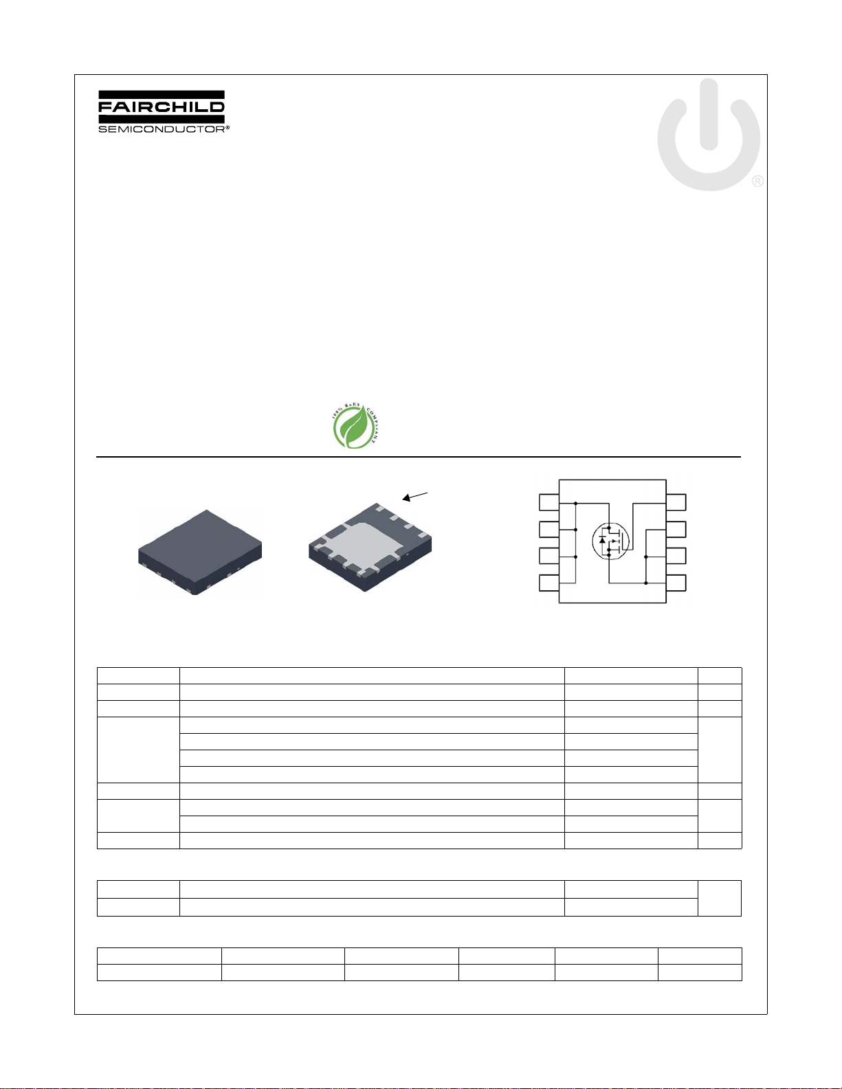
Top
Power 56
DS(on)
Bottom
S
D
D
D
D
General Description
This N-Channel MOSFET has been designed specifically to
improve the overall efficiency and to minimize switch node
ringing of DC/DC converters using either synchronous or
conventional switching PWM controllers. It has been optimized
for low gate charge, low r
diode reverse recovery performance.
fast switching speed and body
DS(on),
Applications
IMVP Vcore Switching for Notebook
VRM Vcore Switching for Desktop and Server
OringFET / Load Switch
DC-DC Conversion
Pin 1
S
S
G
D
5
D
6
D
7
8
D
4
3
2
1
®
MOSFET
G
S
S
S
MOSFET Maximum Ratings T
Symbol Parameter Ratings Units
V
DS
V
GS
I
D
E
AS
P
D
, T
T
J
STG
Drain to Source Voltage 30 V
Gate to Source Voltage ±20 V
Drain Current -Continuous (Package limited) TC = 25 °C 28
-Continuous (Silicon limited) T
-Continuous T
-Pulsed 50
Single Pulse Avalanche Energy (Note 3) 21 mJ
Power Dissipation TC = 25 °C 27
Power Dissipation T
Operating and Storage Junction Temperature Range -55 to +150 °C
A
Thermal Characteristics
R
θJC
R
θJA
Thermal Resistance, Junction to Case 4.6
Thermal Resistance, Junction to Ambient (Note 1a) 50
Package Marking and Ordering Information
Device Marking Device Package Reel Size Tape Width Quantity
FDMS7692A FDMS7692A Power 56 13 ’’ 12 mm 3000 units
©2009 Fairchild Semiconductor Corporation
FDMS7692A Rev.B
= 25 °C unless otherwise noted
= 25 °C 45
C
= 25 °C (Note 1a) 13.5
A
= 25 °C (Note 1a) 2.5
A
1
A
W
°C/W
www.fairchildsemi.com
Page 2
FDMS7692A N-Channel PowerTrench
Electrical Characteristics T
= 25 °C unless otherwise noted
J
Symbol Parameter Test Conditions Min Typ Max Units
Off Characteristics
BV
∆BV
∆T
I
DSS
I
GSS
DSS
DSS
J
Drain to Source Breakdown Voltage ID = 250 µA, VGS = 0 V 30 V
Breakdown Voltage Temperature
Coefficient
Zero Gate Voltage Drain Current VDS = 24 V, V
Gate to Source Leakage Current, Forward VGS = 20 V, V
I
= 250 µA, referenced to 25 °C 13 mV/°C
D
= 0 V 1 µA
GS
= 0 V 100 nA
DS
On Characteristics
V
GS(th)
∆V
∆T
r
DS(on)
g
FS
GS(th)
J
Gate to Source Threshold Voltage VGS = VDS, ID = 250 µA 1.0 2.0 3.0 V
Gate to Source Threshold Voltage
Temperature Coefficient
Static Drain to Source On Resistance
I
= 250 µA, referenced to 25 °C -6 mV/°C
D
V
= 10 V, ID = 13 A 6.8 8
GS
= 4.5 V, ID = 10 A 10 14
GS
= 10 V, ID = 13 A, TJ = 125 °C 9.5 12
V
GS
Forward Transconductance VDS = 5 V, ID = 13 A 68 S
Dynamic Characteristics
C
iss
C
oss
C
rss
R
g
Input Capacitance
Output Capacitance 325 435 pF
Reverse Transfer Capacitance 45 65 pF
Gate Resistance 1.5 3.0 Ω
Switching Characteristics
t
d(on)
t
r
t
d(off)
t
f
Q
Q
Q
Q
g
g
gs
gd
Turn-On Delay Time
Rise Time 2.7 10 ns
Turn-Off Delay Time 17 31 ns
Fall Time 2.3 10 ns
Total Gate Charge VGS = 0 V to 10 V
Total Gate Charge VGS = 0 V to 4.5 V 7 10 nC
Gate to Source Charge 3.4 nC
Gate to Drain “Miller” Charge 1.9 nC
= 15 V, VGS = 0 V,
V
DS
f = 1 MHz
= 15 V, ID = 13 A,
V
DD
V
= 10 V, R
GS
GEN
= 6 Ω
V
DD
I
= 13 A
D
= 15 V,
1015 1350 pF
816ns
15 22 nC
mΩV
®
MOSFET
Drain-Source Diode Characteristics
V
SD
t
rr
Q
rr
t
rr
Q
rr
Notes:
1. R
is determined with the device mounted on a 1i n2 pad 2 oz copper pad on a 1.5 x 1.5 in. board of FR-4 material. R
θJA
the user's board design.
2. Pulse Test: Pulse Width < 300 µs, Duty cycle < 2.0%.
3. Starting TJ = 25 °C, L = 0.3 mH, IAS = 12 A, VDD = 27 V, VGS = 10 V.
©2009 Fairchild Semiconductor Corporation
FDMS7692A Rev.B
Source to Drain Diode Forward Voltage
Reverse Recovery Time
Reverse Recovery Charge 6 12 nC
Reverse Recovery Time
Reverse Recovery Charge 12 21 nC
a. 50 °C/W when mounted on a
2
1 in
pad of 2 oz copper.
V
= 0 V, IS = 2.1 A (Note 2) 0.75 1.1
GS
= 0 V, IS = 13 A (Note 2) 0.84 1.2
V
GS
= 13 A, di/dt = 100 A/µs
I
F
= 13 A, di/dt = 300 A/µs
I
F
2
θJC
21 34 ns
17 31 ns
is guaranteed by design while R
b. 125 °C/W when mounted on a
minimum pad of 2 oz copper.
V
is determined by
θCA
www.fairchildsemi.com
Page 3
FDMS7692A N-Channel PowerTrench
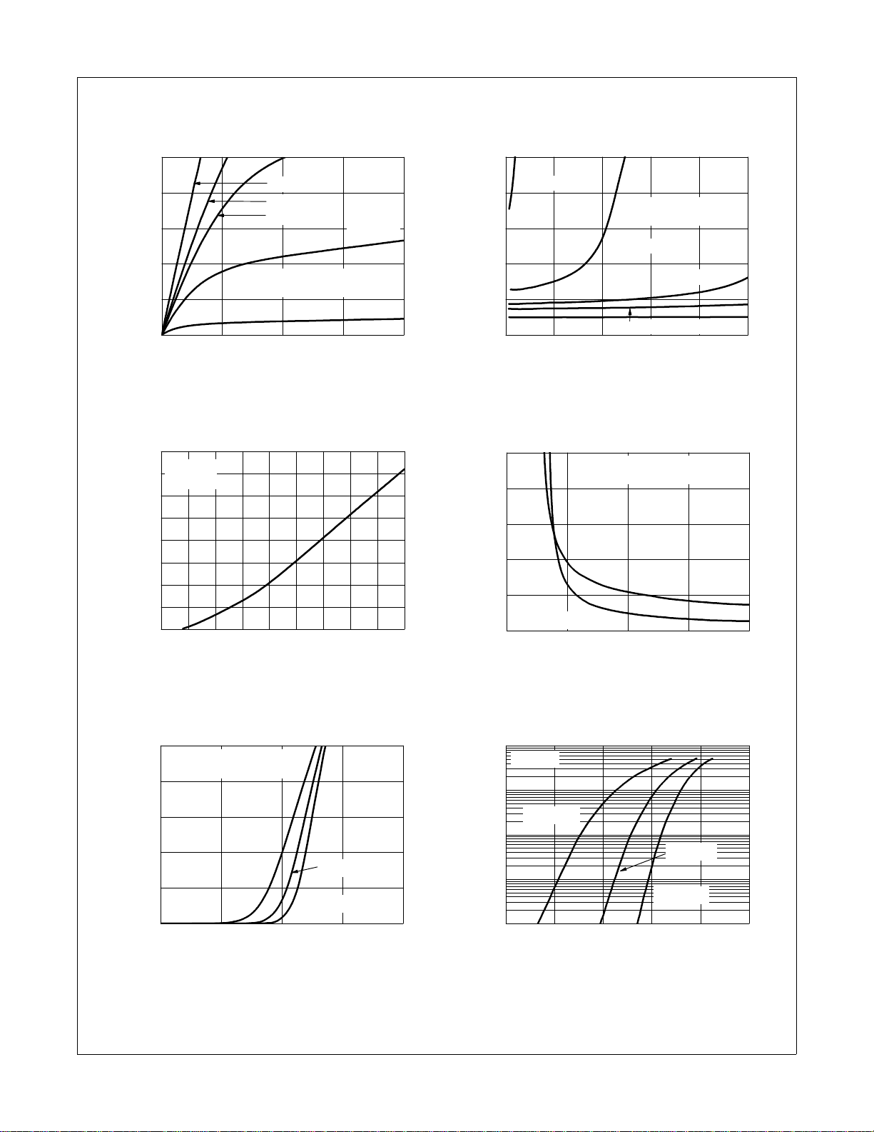
Typical Characteristics T
50
40
30
20
DRAIN CURRENT (A)
,
10
D
I
0
0.0 0.5 1.0 1.5 2.0
V
,
DRAIN TO SOURCE VOLTAGE (V)
DS
Figure 1.
On Region Characteristics Figure 2.
1.6
ID = 13 A
1.5
V
= 10 V
GS
1.4
1.3
1.2
1.1
NORMALIZED
1.0
0.9
DRAIN TO SOURCE ON-RESISTANCE
0.8
-75 -50 -25 0 25 50 75 100 125 150
T
,
JUNCTION TEMPERATURE
J
VGS = 10 V
VGS = 4.5 V
VGS = 4.0 V
PULSE DURATION = 80 µs
DUTY CYCLE = 0.5% MAX
= 25 °C unless otherwise noted
J
VGS = 3.5 V
VGS = 3.0 V
o
(
C
)
10
VGS = 3.0 V
NORMALIZED
8
6
4
PULSE DURATION = 80 µs
DUTY CYCLE = 0.5% MAX
VGS = 3.5 V
VGS = 4.0 V
2
DRAIN TO SOURCE ON-RESISTANCE
0
0 1020304050
VGS = 4. 5 V
I
,
DRAIN CURRENT (A)
D
V
= 10 V
GS
Norma li zed On -R esi st ance
vs Drain Current and Gate Voltage
30
)
Ω
m
25
(
ID = 13 A
20
DRAIN TO
,
15
DS(on)
r
10
SOURCE ON-RESISTANCE
5
246810
TJ = 25 oC
V
,
GATE TO SOURCE VOLTAGE (V)
GS
PULSE DURATION = 80 µs
DUTY CYCLE = 0.5% MAX
TJ = 125 oC
®
MOSFET
Fi gu re 3. Normalized O n R es istance
vs Junction Temperature
50
PULSE DURATION = 80 µs
DUTY CYCLE = 0.5% MAX
40
V
= 5 V
DS
30
20
, DRAIN CURRENT (A)
10
D
I
0
12345
TJ = 150 oC
VGS, GATE TO SOURC E V OLTAGE (V)
Figure 5. Transfer Characteristics
©2009 Fairchild Semiconductor Corporation
FDMS7692A Rev.B
TJ = 25 oC
TJ = -55 oC
Figure 4.
On-Resistance vs Gate to
Source Voltage
100
V
= 0 V
GS
10
TJ = 150 oC
1
TJ = 25 oC
0.1
, REVERSE DRAIN CURRENT (A)
S
I
0.01
0.2 0.4 0.6 0.8 1.0 1.2
VSD, BODY DIODE FORWARD VOLTAGE (V)
Figure 6.
Sou rce to Dr ain Diode
TJ = -55 oC
Forward Voltage vs Source Current
3
www.fairchildsemi.com
Page 4

FDMS7692A N-Channel PowerTrench
Typical Characteristics T
10
ID = 13 A
8
V
= 15 V
DD
6
4
2
, GATE TO SOURCE VOLTAGE (V)
GS
V
0
0481216
Figure 7.
50
10
, AVALANCHE CURRENT (A)
AS
I
1
0.001 0.01 0.1 1 10 100
VDD = 10 V
Qg, GATE CHARGE (nC)
Gate Charge Characteristics Figure 8.
TJ = 25 oC
TJ = 125 oC
tAV, TIME IN AVALANCHE (ms )
= 25 °C unless otherwise noted
J
VDD = 20 V
TJ = 100 oC
2000
1000
100
CAPACITANCE (pF)
f = 1 MHz
V
= 0 V
GS
10
0.1 1 10 30
VDS, DRAIN TO SOURCE VOL TA G E (V)
Cap ac ita nce vs Dra in
to Source Voltage
50
40
30
20
DRAIN CURRENT (A)
Limited by Package
,
D
I
10
R
= 4.6 oC/W
θ
JC
0
25 50 75 100 125 150
T
,
CASE TEMPERATURE
C
V
= 4.5 V
GS
o
(
C
C
iss
C
oss
C
rss
®
MOSFET
V
= 10 V
GS
)
Figure 9.
Unc lam ped Ind u ct i ve
Switching Capability
100
10
1
, DRAIN CURRENT (A)
D
I
THIS AREA IS
LIMITED BY r
0.1
0.01
0.01 0.1 1 10 100
DS(on)
SINGLE PULSE
= MAX RATED
T
J
= 125 oC/W
R
θ
JA
= 25 oC
T
A
VDS, DRAIN to SOURCE VOLTAGE (V)
Figure 11. Forward Bias Safe
Operating Area
©2009 Fairchild Semiconductor Corporation
FDMS7692A Rev.B
Figure 10.
Ma xim um Contin uous Drai n
Current vs Case Temperature
300
100
100 us
1 ms
10 ms
100 ms
1 s
10 s
DC
200
10
PEAK TRANSIENT POWER (W)
,
)
PK
(
P
0.5
VGS = 10 V
1
10-410-310-210
t, PULSE WIDTH (sec)
Figure 12.
Single Pulse Maximum
-1
SINGLE PULSE
R
= 125 oC/W
θ
JA
= 25 oC
T
A
110
100 1000
Power Dissipation
4
www.fairchildsemi.com
Page 5

FDMS7692A N-Channel PowerTrench
Typical Characteristics T
2
DUTY CYCLE-DESCENDING ORDER
1
D = 0.5
0.2
JA
θ
Z
0.1
IMPEDANCE,
0.01
NORMALIZED THERMAL
0.001
14
12
10
8
6
4
CURRENT (A)
2
0
-2
0 20406080100
Figure 14.
0.1
0.05
0.02
0.01
-4
10
-3
10
Figure 13.
di/dt = 300 A/µs
TIME (ns)
Bo dy Diode Re verse
Recovery Characteristics
= 25 °C unless otherwise noted
J
NOTES:
SINGLE PULSE
= 125 oC/W
R
θ
JA
-2
10
-1
10
t, RECTANGULAR PULSE DURATION (sec)
110
DUTY FACTOR: D = t
PEAK TJ = PDM x Z
Junction-to-Ambient Transient Thermal Response Curve
Figure 15.
P
DM
t
1
t
2
1/t2
x R
+ T
θJA
θJA
A
100 1000
®
MOSFET
©2009 Fairchild Semiconductor Corporation
FDMS7692A Rev.B
5
www.fairchildsemi.com
Page 6

Dimensional Outline and Pad Layout
FDMS7692A N-Channel PowerTrench
®
MOSFET
©2009 Fairchild Semiconductor Corporation
FDMS7692A Rev.B
6
www.fairchildsemi.com
Page 7

TRADEMARKS
tm
®
tm
tm
The following includes registered and unregistered trademarks and service marks, owned by Fairchild Semicond uctor and/or its gl obal subsidiaries, a nd is not
intended to be an exhaustive list of all such trademarks.
Auto-SPM™
Build it Now™
CorePLUS™
CorePOWER™
CROSSVOLT™
CTL™
Current Transfer Logic™
EcoSPARK
EfficentMax™
EZSWITCH™ *
™*
Fairchild
Fairchild Semiconductor
FACT Quiet Series™
FACT
FAST
FastvCore™
FETBench™
FlashWriter
FPS™
®
®
®
®
®
*
®
F-PFS™
FRFET
Global Power Resource
Green FPS™
Green FPS™ e-Series™
Gmax™
GTO™
IntelliMAX™
ISOPLANAR™
MegaBuck™
MICROCOUPLER™
MicroFET™
MicroPak™
MillerDrive™
MotionMax™
Motion-SPM™
OPTOLOGIC
OPTOPLANAR
®
PDP SPM™
Power-SPM™
®
SM
PowerTrench
PowerXS™
Programmable Active Droop™
QFET
QS™
Quiet Series™
RapidConfigure™
Saving our world, 1mW /W /kW at a time™
SmartMax™
SMART START™
SPM
STEALTH™
SuperFET™
®
®
SuperSOT™-3
SuperSOT™-6
SuperSOT™-8
SupreMOS™
SyncFET™
Sync-Lock™
®
®
™
®
The Power Franchise
TinyBoost™
TinyBuck™
TinyLogic
TINYOPTO™
TinyPower™
TinyPWM™
TinyWire™
TriFault Detect™
TRUECURRENT™*
®
®
®
µSerDes™
®
UHC
Ultra FRFET™
UniFET™
VCX™
VisualMax™
®*
XS™
*Trademarks of System General Corporation, used under license by Fairchild Semiconductor.
DISCLAIMER
FAIRCHILD SEMICONDUCTOR RESERVES THE RIGHT TO MAKE CHANGES WITHOUT FURTHER NOTICE TO ANY PRODUCTS HEREIN TO IMPROVE
RELIABILITY, FUNCTION, OR DESIGN. FAIRCHILD DOES NOT ASSUME ANY LIABILITY ARISING OUT OF THE APPLICATION OR USE OF ANY
PRODUCT OR CIRCUIT DESCRIBED HEREIN; NEITHER DOES IT CONVEY ANY LICENSE UNDER ITS PATENT RIGHTS, NOR THE RIGHTS OF OTHERS.
THESE SPECIFICATIONS DO NOT EXPAND THE TERMS OF FAIRCHILD’S WORLDWIDE TERMS AND CONDITIONS, SPECIFICALLY THE WARRANTY
THEREIN, WHICH COVERS THESE PRODUCTS.
FDMS7692A N-Channel PowerTrench
®
MOSFET
LIFE SUPPORT POLICY
FAIRCHILD’S PRODUCTS ARE NOT AUTHORIZED FOR USE AS CRITICAL COMPONENTS IN LIFE SUPPORT DEVICES OR SYSTEMS WITHOUT THE
EXPRESS WRITTEN APPROVAL OF FAIRCHILD SEMICONDUCTOR CORPORATION.
As used herein:
1. Life support devices or systems are devices or systems which, (a) are
intended for surgical implant into the bo dy or (b ) sup port or sust ain li fe,
and (c) whose failure to perform when properly used in accordance with
instructions for use provided in the labeling, can be reasonably
expected to result in a significant injury of the user.
ANTI-COUNTERFEITING POLICY
Fairchild Semiconductor Corporation’s Anti-Counterfeiting Policy. Fairchild’s Anti-Counterfeiting Policy is also stated on our external website,
www.Fairchildsemi.com, under Sales Support
Counterfeiting of semiconductor parts is a growing problem in the industry. Al l manufactures of semiconductor products are exper iencing counterfeiting of th eir
parts. Customers who inadvertently purchase counterfeit parts experience many probl ems such a s loss of b rand rep uta tion, subst an dar d perf orman ce, fai led
application, and increased cost of production and manufacturing delays. Fairchi ld is t aking stro ng measures to protect ourselves and our customers from the
proliferation of counterfeit parts. Fairchild st rongly encour ages customers to purcha se Fairchild parts either directly from Fairchild or from Authorized Fairchild
Distributors who are listed by country on our web page cited above. Products customers buy either from Fairchild directly or from Authorized Fairchild
Distributors are genuine parts, have full traceability, meet Fairchild’s quality standards for handing and storage and provide access to Fairchild’s full range of
up-to-date technical and product information. Fairchild and our Authorized Distributors will stand behind all warranties and will appropriately address and
warranty issues that may arise. Fairchild will not provide any warranty coverage or other assistance for part s bought from Unauthorized Sources. Fairchild is
committed to combat this global problem and encourage our customers to do their part in stopping this practi ce by buying direct or from authorized distributors.
PRODUCT STATUS DEFINITIONS
Definition of Terms
.
2. A critical component in any component of a life support, device, or
system whose failure to perform can be reasonably expected to cause
the failure of the life support device or system, or to affect its safety or
effectiveness.
Datasheet Identification Product Status Definition
Advance Information Formative / In Design
Preliminary First Production
No Identification Needed Full Production
Obsolete Not In Production
Datasheet contains the design specifications for product development. Specifications
may change in any manner without notice.
Datasheet contains preliminary data; supplementary data will be published at a later
date. Fairchild Semiconductor reserves the right to make changes at any time without
notice to improve design.
Datasheet contains final specifications. Fairchild Semiconductor reserves the right to
make changes at any time without notice to improve the design.
Datasheet contains specifications on a product that is discontinued by Fairchild
Semiconductor. The datash eet is for reference information only.
Rev. I40
©2009 Fairchild Semiconductor Corporation 7 www.fairchildsemi.com
FDMS7692A Rev.B
 Loading...