

Page 1
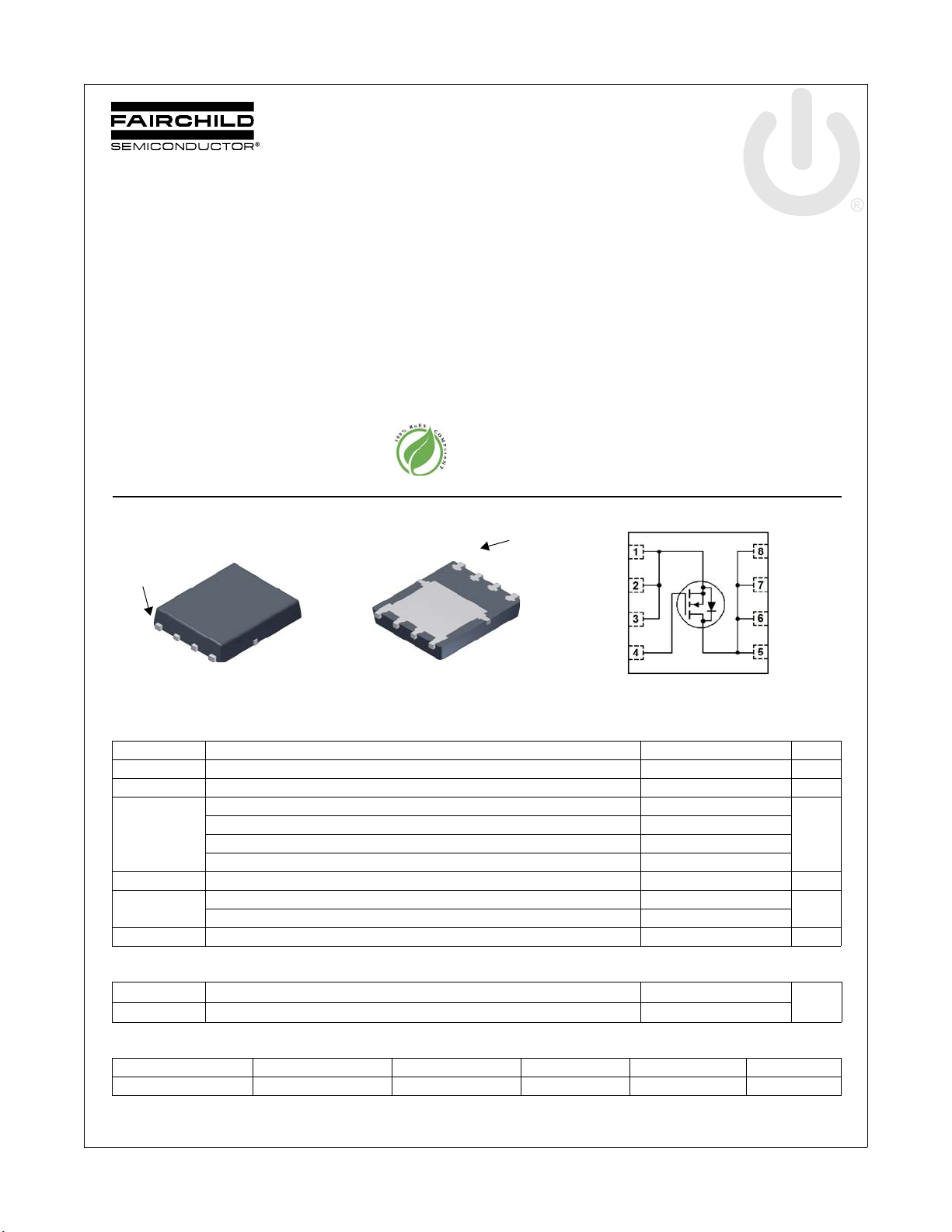
FDMS7678
Power 56
D
D
D
D
G
S
S
S
Pin 1
Bottom
Top
D
D
D
D
S
S
S
G
Pin 1
N-Channel Power Trench® MOSFET
30 V, 26 A, 5.5 mΩ
Features
Max r
Max r
High performance technology for extremely low r
Termination is Lead-free
RoHS Compliant
= 5.5 mΩ at VGS = 10 V, ID = 17.5 A
DS(on)
= 6.8 mΩ at VGS = 4.5 V, ID = 15 A
DS(on)
DS(on)
General Description
This N-Channel MOSFET is produced using Fairchild
Semiconductor’s advanced Power
been especially tailored to minimize the on-state resistance.
device is well suited for Power Management and load switching
applications common in Notebook Computers and Portable
Battery Packs.
Applications
DC - DC Buck Converters
Notebook battery power management
Load switch in Notebook
FDMS7678 N-Channel Power Trench
April 2012
Trench® process that has
This
®
MOSFET
MOSFET Maximum Ratings T
Symbol Parameter Ratings Units
V
DS
V
GS
I
D
E
AS
P
D
, T
T
J
STG
Drain to Source Voltage 30 V
Gate to Source Voltage (Note 3) ±20 V
Drain Current -Continuous (Package limited) TC = 25 °C 26
Drain Current -Continuous (Silicon limited) T
-Continuous T
-Pulsed 70
Single Pulse Avalanche Energy (Note 4) 54 mJ
Power Dissipation TC = 25 °C 41
Power Dissipation T
Operating and Storage Junction Temperature Range -55 to +150 °C
= 25 °C unless otherwise noted
A
= 25 °C 72
C
= 25 °C (Note 1a) 17.5
A
= 25 °C (Note 1a) 2.3
A
A
W
Thermal Characteristics
R
θJC
R
θJA
Package Marking and Ordering Information
Device Marking Device Package Reel Size Tape Width Quantity
FDMS7678 FDMS7678 Power 56 13 ’’ 12 mm 3000 units
©2012 Fairchild Semiconductor Corporation
FDMS7678 Rev. C1
Thermal Resistance, Junction to Case 3
Thermal Resistance, Junction to Ambient (Note 1a) 50
1
°C/W
www.fairchildsemi.com
Page 2
Electrical Characteristics T
= 25 °C unless otherwise noted
J
Symbol Parameter Test Conditions Min Typ Max Units
Off Characteristics
BV
ΔBV
ΔT
I
DSS
I
GSS
DSS
DSS
J
Drain to Source Breakdown Voltage ID = 250 μA, VGS = 0 V 30 V
Breakdown Voltage Temperature
Coefficient
Zero Gate Voltage Drain Current VDS = 24 V, V
Gate to Source Leakage Current, Forward VGS = 20 V, V
I
= 250 μA, referenced to 25 °C 21 mV/°C
D
= 0 V 1 μA
GS
= 0 V 100 nA
DS
On Characteristics
V
GS(th)
ΔV
ΔT
r
DS(on)
g
FS
GS(th)
J
Gate to Source Threshold Voltage VGS = VDS, ID = 250 μA 1.2 1.5 3.0 V
Gate to Source Threshold Voltage
Temperature Coefficient
Static Drain to Source On Resistance
I
= 250 μA, referenced to 25 °C -5 mV/°C
D
V
= 10 V, ID = 17.5 A 4.7 5.5
GS
= 4.5 V, ID = 15 A 5.6 6.8
GS
= 10 V, ID = 17.5 A TJ = 125 °C 6.3 7.4
V
GS
Forward Transconductance VDD = 5 V, ID = 17.5 A 90 S
Dynamic Characteristics
C
iss
C
oss
C
rss
R
g
Input Capacitance
Output Capacitance 620 820 pF
Reverse Transfer Capacitance 75 110 pF
= 15 V, VGS = 0 V
V
DS
f = 1 MHz
Gate Resistance 0.1 0.7 2.5 Ω
1810 2410 pF
FDMS7678 N-Channel Power Trench
mΩV
®
MOSFET
Switching Characteristics
t
d(on)
t
r
t
d(off)
t
f
Q
g(TOT)
Q
gs
Q
gd
Turn-On Delay Time
Rise Time 410ns
Turn-Off Delay Time 26 41 ns
= 15 V, ID = 17.5 A
V
DD
V
= 10 V, R
GS
GEN
= 6 Ω
Fall Time 310ns
Total Gate Charge VGS = 0 V to 10 V
Total Gate Charge V
= 0 V to 4.5 V 14 19 nC
GS
Gate to Source Charge 4.4 nC
Gate to Drain “Miller” Charge 3.9 nC
Drain-Source Diode Characteristics
V
= 0 V, IS = 1.9 A (Note 2) 0.7 1.2
V
SD
t
rr
Q
rr
NOTES:
1. R
is determined with the device mounted on a 1 in2 pad 2 oz copper pad on a 1.5 x 1.5 in. board of FR-4 material. R
θJA
the user's board design.
Source to Drain Diode Forward Voltage
Reverse Recovery Time
Reverse Recovery Charge 13 23 nC
a. 50 °C/W when mounted on
2
a 1 i n
GS
= 0 V, IS = 17.5 A (Note 2) 0.8 1.2
V
GS
= 17.5 A, di/dt = 100 A/μs
I
F
p a d o f 2 o z c o p p e r
= 15 V
V
DD
I
= 17.5 A
D
10 19 ns
28 39 nC
30 49 ns
is guaranteed by design while R
θJC
b.125 °C/W when mounted on
a minimum pad of 2 oz copper
is determined by
θCA
V
DS
DF
G
2. Pulse Test: Pulse Width < 300 μs, Duty cycle < 2.0 %.
3. As an N-ch device, the negative V
4. E
of 54 mJ is based on starting TJ = 25 oC, L = 0.3 mH, IAS = 19 A, VDD = 27 V, VGS = 10 V.
AS
©2012 Fairchild Semiconductor Corporation
FDMS7678 Rev. C1
rating is for low duty cycle pulse occurence only. No continuous rating is implied.
GS
SF
SS
SF
SS
DS
DF
G
2
www.fairchildsemi.com
Page 3
FDMS7678 N-Channel Power Trench
0.0 0.5 1.0 1.5 2.0
0
10
20
30
40
50
60
70
VGS = 3 V
VGS = 3.5 V
VGS = 4.5 V
PULSE DURATION = 80 μs
DUTY CYCLE = 0.5% MAX
VGS = 6 V
VGS = 10 V
I
D
, DRAIN CURRENT (A)
V
DS
, DRAIN TO SOURCE VOLTAGE (V)
0 10203040506070
0
1
2
3
4
VGS = 3 V
VGS = 6 V
PULSE DURATION = 80 μs
DUTY CYCLE = 0.5% MAX
NORMALIZED
DRAIN TO SOURCE ON-RESISTANCE
I
D
, DRAIN CURRENT (A)
VGS = 3.5 V
VGS = 4.5 V
V
GS
= 10 V
-75 -50 -25 0 25 50 75 100 125 150
0.7
0.8
0.9
1.0
1.1
1.2
1.3
1.4
1.5
ID = 17.5 A
V
GS
= 10 V
NORMALIZED
DRAIN TO SOURCE ON-RESISTANCE
T
J
, JUNCTION TEMPERATURE (
o
C)
246810
3
6
9
12
15
TJ = 125 oC
ID = 17.5 A
TJ = 25 oC
V
GS
, GATE TO SOURCE VOLTAGE (V)
r
DS(on)
,
DRAIN TO
SOURCE ON-RESISTANCE
(mΩ)
PULSE DURATION = 80 μs
DUTY CYCLE = 0.5% MAX
1.0 1.5 2.0 2.5 3.0 3.5
0
10
20
30
40
50
60
70
TJ = 150 oC
V
DS
= 5 V
PULSE DURATION = 80 μs
DUTY CYCLE = 0.5% MAX
TJ = -55 oC
TJ = 25 oC
I
D
, DRAIN CURRENT (A)
VGS, GATE TO SOURCE VOLTAG E (V)
0.0 0.2 0 .4 0.6 0.8 1.0 1.2
0.001
0.01
0.1
1
10
100
TJ = -55 oC
TJ = 25 oC
TJ = 150 oC
V
GS
= 0 V
I
S
, REVERSE DRAIN CURRENT (A)
VSD, BODY DIODE FORWARD VOLTAGE (V)
Typical Characteristics T
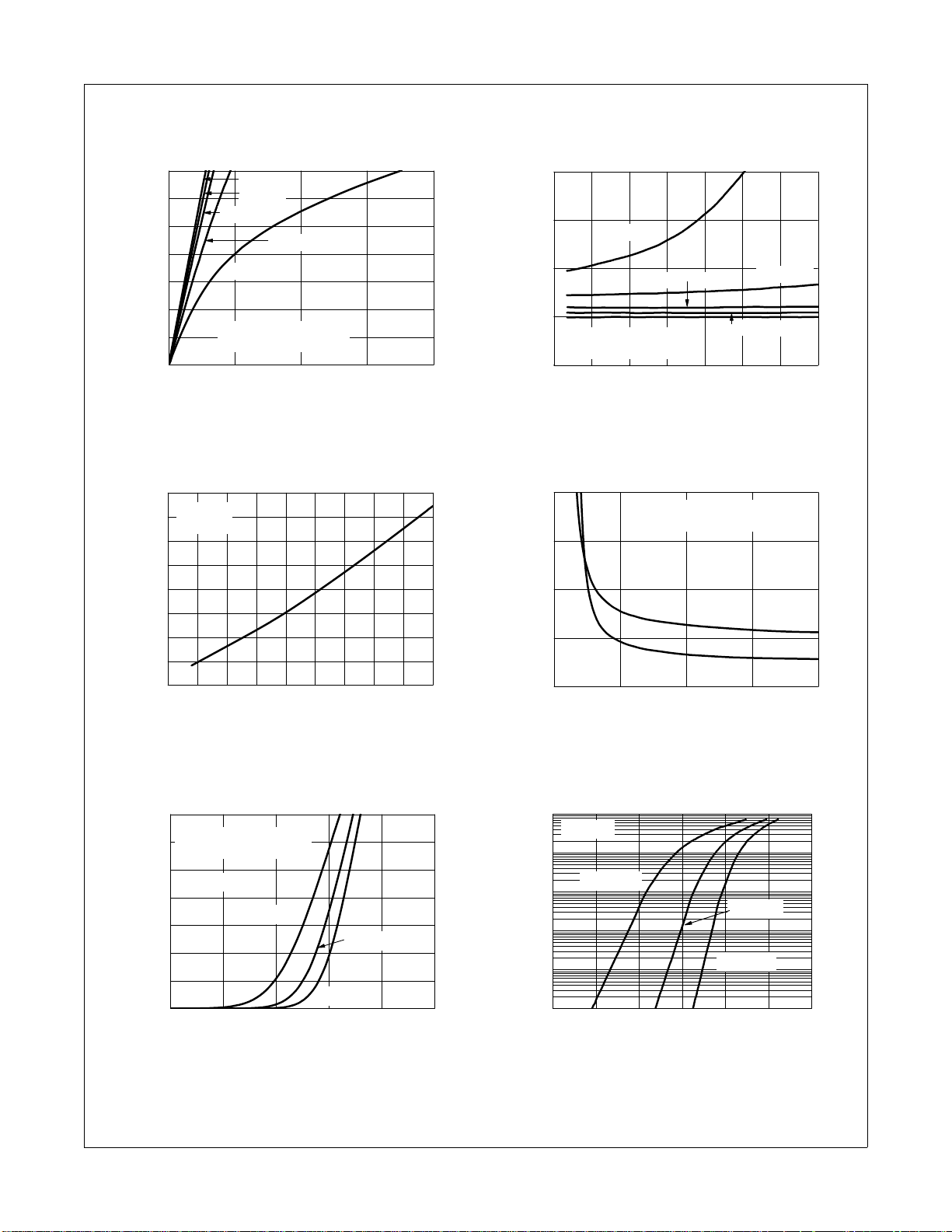
Figure 1.
On Region Characteristics
= 25 °C unless otherwise noted
J
Figure 2.
Normalized On-Resista nc e
vs Drain Current and Gate Voltage
®
MOSFET
Fi g ure 3 . Norm a l ized O n Res i stan c e
vs Junction Temperature
©2012 Fairchild Semiconductor Corporation
FDMS7678 Rev. C1
Figure 5. Transfer Characteristics
Figure 4.
On-Resi stance vs Gate to
Source Voltage
Figure 6.
Sou rce t o Drain Diode
Forward Voltage vs Source Current
3
www.fairchildsemi.com
Page 4

FDMS7678 N-Channel Power Trench
0 5 10 15 20 25 30
0
2
4
6
8
10
ID = 17.5 A
VDD = 20 V
V
DD
= 10 V
V
GS
, GATE TO SOURCE VOLTAGE (V)
Qg, GATE CHARGE (nC)
VDD = 15 V
0.1 1 10 30
30
100
1000
3000
f = 1 MHz
V
GS
= 0 V
CAPACITANCE (pF)
VDS, DRAIN TO SOURCE VOLTAGE (V)
C
rss
C
oss
C
iss
0.001 0.01 0.1 1 10 100
1
10
30
TJ = 100 oC
TJ = 25 oC
TJ = 125 oC
tAV, TIME IN AVALANCHE (ms)
I
AS
, AVALANCHE CURRENT (A)
25 50 75 100 125 150
0
20
40
60
80
Limited by Package
V
GS
= 4.5 V
R
θJC
= 3.0 oC/W
V
GS
= 10 V
I
D
, DRAIN CURRENT (A)
T
C
, CASE TEMPERATURE (
o
C)
0.01 0.1 1 10 100200
0.01
0.1
1
10
100
100 μs
10 ms
10 s
100 ms
DC
1 s
1 ms
I
D
, DRAIN CURRENT (A)
VDS, DRAIN to SOURCE VOLTAGE (V)
THIS AREA IS
LIMITED BY r
DS(on)
SINGLE PULSE
T
J
= MAX RATED
R
θJA
= 125
o
C/W
T
A
= 25
o
C
10-410-310-210
-1
110
100 1000
0.5
1
10
100
1000
SINGLE PULSE
R
θJA
= 125
o
C/W
T
A
= 25
o
C
P(
PK
), PEAK TRANSIENT POWER (W)
t, PULSE WIDTH (sec)
Typical Characteristics T
Figure 7.
Gate Charge Characteristics Figure 8.
= 25 °C unless otherwise noted
J
®
MOSFET
Capaci t a n c e v s Drain
to Source Voltage
Figure 9.
Unc l a m ped I n d uc t i v e
Switching Capability
©2012 Fairchild Semiconductor Corporation
FDMS7678 Rev. C1
Figure 11. Forward Bias Safe
Op
erating Area
Figure 10.
Ma ximum Con tin uou s Drai n
Current vs Case Temperature
Figure 12.
Single Pulse Ma ximum
Power Dissipation
4
www.fairchildsemi.com
Page 5

FDMS7678 N-Channel Power Trench
10
-4
10
-3
10
-2
10
-1
110
100 1000
0.001
0.01
0.1
1
2
D = 0.5
0.2
0.1
0.05
0.02
0.01
SINGLE PULSE
R
θJA
= 125 oC/W
DUTY CYCLE-DESCENDING ORDER
NORMALIZED THERMAL
IMPEDANCE,
Z
θJA
t, RECTANGULAR PULSE DURATION (sec)
P
DM
t
1
t
2
NOTES:
DUTY FACTOR: D = t1/t
2
PEAK TJ = PDM x Z
θJA
x R
θJA
+ T
A
Typical Characteristics T
Figure 13. Junction-to-Ambient Transient Thermal Response Curve
= 25 °C unless otherwise noted
J
®
MOSFET
©2012 Fairchild Semiconductor Corporation
FDMS7678 Rev. C1
5
www.fairchildsemi.com
Page 6

Dimensional Outline and Pad Layout
C
L
L
C
PKG
PKG
5.1 0
4.90
6.25
5.90
C
1.2 7
3.8 1
3.8 6
3.6 1
0.71
0.44
CHA MFE R
CORNER
AS PIN #1
IDEN T MAY
APPEAR AS
OPTIONAL
TOP VIEW
SIDE VIEW
BOTTOM VIEW
1.27
3.81
1.2 7
6.6 1
3.91
4.52
1.27
1234
8567
1
4
8
5
LAND PA TTERN
RECOMMENDATION
12 34
876
0.10 C A B
0.46
0.36
(8X)
4.2 9
4.0 9
5
0.71
0.44
0.77
A
B
(0.39)
0.61
NOTES: UNLESS OTHERWISE SPECIFIED
A) PACKAGE STANDARD REFE RENCE:
JEDEC MO-240, ISSUE A, VAR. AA,
DATED OCTOBER 2002.
B) ALL DIMENSIONS ARE IN MILLIMETERS.
C) DIMENSIONS DO NOT INCLUDE BURRS
OR MOLD FLASH. MOLD FLASH OR
BURRS DOES NOT EXCEED 0.10MM.
D) DIMENSIONING AND TOLERANCING PER
ASME Y14.5M-1994.
E) IT IS RECOMMENDED TO HAVE NO TRACES
OR VIAS WITHIN THE KEEP OUT AREA.
F) DRAWING FILE NAME: PQFN08AREV6.
SEE
DETAIL A
DETAIL A
SCALE: 2:1
0.05
0.00
0.30
0.20
0.08 C
6.25
5.90
5.85
5.65
5.1 0
4.90
6
OPTIONAL DRAFT
ANGLE MAY APPEAR
ON FOUR SIDES
OF THE PACKAGE
PIN #1
IDEN T MAY
APPEAR AS
OPTIONAL
SEATING
PLANE
0.10 C
1.10
0.90
OPTION - A (SAWN TYPE )
OPTION - B (PUNCHED TYPE)
KEEP OUT AREA
(1.19)
(1.81)
(0.50)
(3.40)
(0.52)
0.1 5 MAX (2 X)
5.10
3.7 5
FDMS7678 N-Channel Power Trench
©2012 Fairchild Semiconductor Corporation
FDMS7678 Rev. C1
6
®
MOSFET
www.fairchildsemi.com
Page 7

TRADEMARKS
®
™
tm
tm
The following includes registered and unregistered trademarks and service marks, owned by Fairchild Semiconductor and/or its global subsidiaries, and is not
intended to be an exhaustive list of all such trademarks.
2Cool™
AccuPower™
AX-CAP™*
®
BitSiC
Build it Now™
CorePLUS™
CorePOWER™
CROSSVOLT™
CTL™
Current Transfer Logic™
DEUXPEED
Dual Cool™
EcoSPARK
EfficentMax™
ESBC™
Fairchild
Fairchild Semiconductor
FACT Quiet Series™
FACT
FAST
FastvCore™
FETBench™
FlashWriter
FPS™
®
®
®
®
®
®
*
®
F-PFS™
®
FRFET
Global Power Resource
Green Bridge™
Green FPS™
Green FPS™ e-Series™
Gmax™
GTO™
IntelliMAX™
ISOPLANAR™
Marking Small Speakers Sound Louder
and Better™
MegaBuck™
MICROCOUPLER™
MicroFET™
MicroPak™
MicroPak2™
MillerDrive™
MotionMax™
Motion-SPM™
mWSaver™
OptoHiT™
OPTOLOGIC
OPTOPLANAR
®
®
®
SM
PowerTrench
PowerXS™
Programmable Active Droop™
QFET
QS™
Quiet Series™
RapidConfigure™
Saving our world, 1mW/W/kW at a time™
SignalWise™
SmartMax™
SMART START™
Solutions for Your Success™
SPM
STEALTH™
SuperFET
SuperSOT™-3
SuperSOT™-6
SuperSOT™-8
SupreMOS
SyncFET™
Sync-Lock™
®
®
®
®
®
®*
The Power Franchise
TinyBoost™
TinyBuck™
TinyCalc™
TinyLogic
TINYOPTO™
TinyPower™
TinyPWM™
TinyWire™
TranSiC
TriFault Detect™
TRUECURRENT
μSerDes™
UHC
Ultra FRFET™
UniFET™
VCX™
VisualMax™
VoltagePlus™
XS™
®
®
®
®
®
®
*
*Trademarks of System General Corporation, used under license by Fairchild Semiconductor.
DISCLAIMER
FAIRCHILD SEMICONDUCTOR RESERVES THE RIGHT TO MAKE CHANGES WITHOUT FURTHER NOTICE TO ANY PRODUCTS HEREIN TO IMPROVE
RELIABILITY, FUNCTION, OR DESIGN. FAIRCHILD DOES NOT ASSUME ANY LIABILITY ARISING OUT OF THE APPLICATION OR USE OF ANY
PRODUCT OR CIRCUIT DESCRIBED HEREIN; NEITHER DOES IT CONVEY ANY LICENSE UNDER ITS PATENT RIGHTS, NOR THE RIGHTS OF OTHERS.
THESE SPECIFICATIONS DO NOT EXPAND THE TERMS OF FAIRCHILD’S WORLDWIDE TERMS AND CONDITIONS, SPECIFICALLY THE WARRANTY
THEREIN, WHICH COVERS THESE PRODUCTS.
FDMS7678 N-Channel Power Trench
®
MOSFET
LIFE SUPPORT POLICY
FAIRCHILD’S PRODUCTS ARE NOT AUTHORIZED FOR USE AS CRITICAL COMPONENTS IN LIFE SUPPORT DEVICES OR SYSTEMS WITHOUT THE
EXPRESS WRITTEN APPROVAL OF FAIRCHILD SEMICONDUCTOR CORPORATION.
As used here in:
1. Life support devices or systems are devices or systems which, (a) are
intended for surgical implant into the body or (b) support or sustain life,
and (c) whose failure to perform when properly used in accordance with
instructions for use provided in the labeling, can be reasonably
expected to result in a significant injury of the user.
ANTI-COUNTERFEITING POLICY
Fairchild Semiconductor Corporation’s Anti-Counterfeiting Policy. Fairchild’s Anti-Counterfeiting Policy is also stated on our external website,
www.Fairchildsemi.com, under Sales Support
Counterfeiting of semiconductor parts is a growing problem in the industry. All manufactures of semiconductor products are experiencing counterfeiting of their
parts. Customers who inadvertently purchase counterfeit parts experience many problems such as loss of brand reputation, substandard performance, failed
application, and increased cost of production and manufacturing delays. Fairchild is taking strong measures to protect ourselves and our customers from the
proliferation of counterfeit parts. Fairchild strongly encourages customers to purchase Fairchild parts either directly from Fairchild or from Authorized Fairchild
Distributors who are listed by country on our web page cited above. Products customers buy either from Fairchild directly or from Authorized Fairchild
Distributors are genuine parts, have full traceability, meet Fairchild’s quality standards for handing and storage and provide access to Fairchild’s full range of
up-to-date technical and product information. Fairchild and our Authorized Distributors will stand behind all warranties and will appropriately address and
warranty issues that may arise. Fairchild will not provide any warranty coverage or other assistance for parts bought from Unauthorized Sources. Fairchild is
.
2. A critical component in any component of a life support, device, or
system whose failure to perform can be reasonably expected to cause
the failure of the life support device or system, or to affect its safety or
effectiveness.
committed to combat this global problem and encourage our customers to do their part in stopping this practice by buying direct or from authorized distributors.
PRODUCT STATUS DEFINITIONS
Definition of Terms
Datasheet Identification Product Status Definition
Advance Information Formative / In Design
Preliminary First Production
No Identification Needed Full Production
Obsolete Not In Production
Datasheet contains the design specifications for product development. Specifications
may change in any manner without notice.
Datasheet contains preliminary data; supplementary data will be published at a later
date. Fairchild Semiconductor reserves the right to make changes at any time without
notice to improve design.
Datasheet contains final specifications. Fairchild Semiconductor reserves the right to
make changes at any time without notice to improve the design.
Datasheet contains specifications on a product that is discontinued by Fairchild
Semiconductor. The datasheet is for reference information only.
Rev. I61
©2012 Fairchild Semiconductor Corporation 7 www.fairchildsemi.com
FDMS7678 Rev. C1
 Loading...