

Page 1
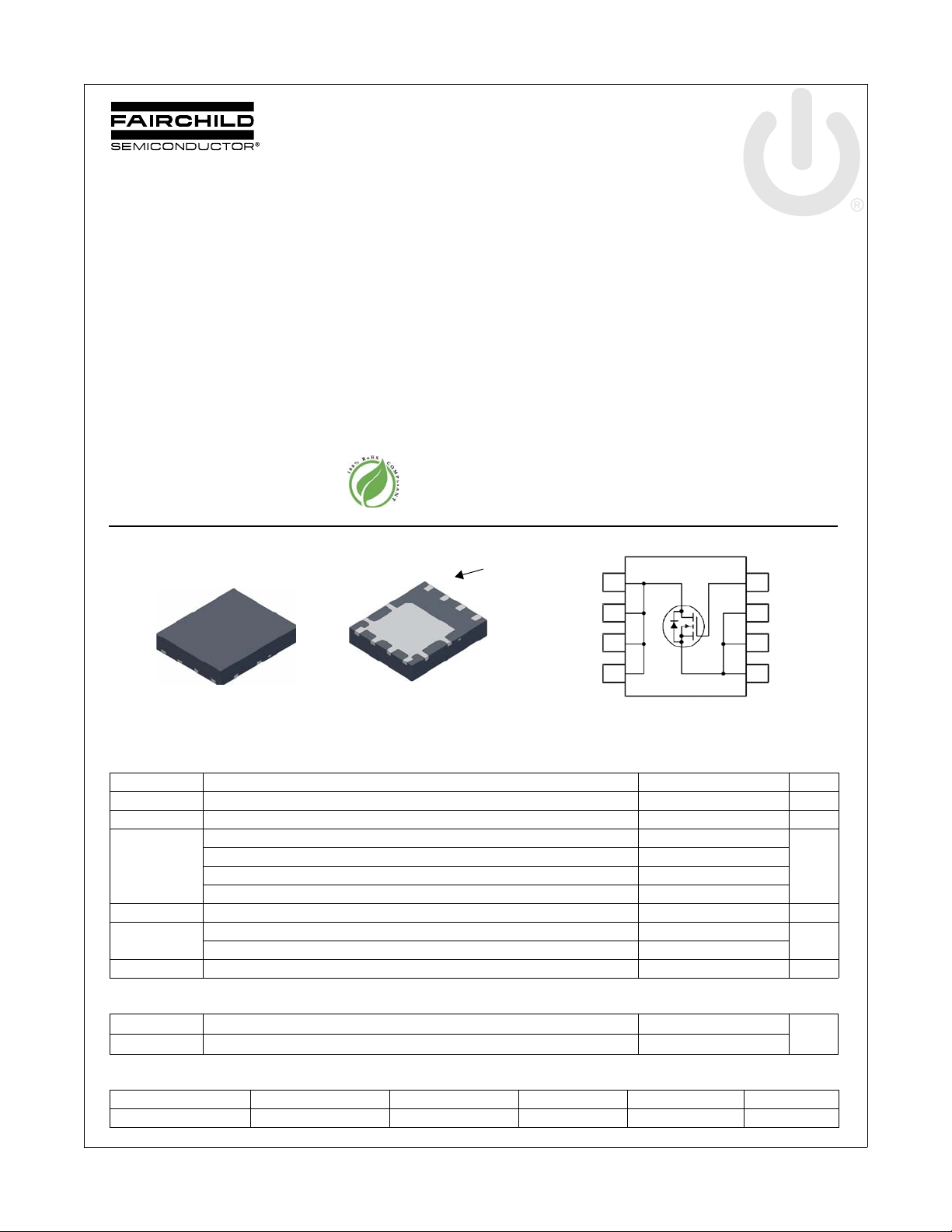
FDMS7670
Bottom
Power 56
Top
Pin 1
G
S
S
S
D
D
D
D
G
S
S
S
D
D
D
D
5
6
7
8
3
2
1
4
N-Channel PowerTrench® MOSFET
30 V, 3.8 mΩ
Features
Max r
Max r
Advanced Package and Silicon design for low r
efficiency
Next generation enhanced body diode technology, engineered
for soft recovery. Provides Schottky-like performance with
minimum EMI in sync buck converter applications
MSL1 robust package design
100% UIL tested
RoHS Compliant
= 3.8 mΩ at VGS = 10 V, ID = 21 A
DS(on)
= 5.0 mΩ at VGS = 4.5 V, ID = 17 A
DS(on)
DS(on)
and high
General Description
This N-Channel MOSFET has been designed specifically to
improve the overall efficiency and to minimize switch node
ringing of DC/DC converters using either synchronous or
conventional switching PWM controllers. It has been optimized
for low gate charge, low r
diode reverse recovery performance.
Applications
IMVP Vcore Switching for Notebook
VRM Vcore Switching for Desktop and Server
OringFET / Load Switch
DC-DC Conversion
July 2012
, fast switching speed and body
DS(on)
FDMS7670 N-Channel PowerTrench
®
MOSFET
MOSFET Maximum Ratings T
Symbol Parameter Ratings Units
V
DS
V
GS
I
D
E
AS
P
D
, T
T
J
STG
Drain to Source Voltage 30 V
Gate to Source Voltage (Note 4) ±20 V
Drain Current -Continuous (Package limited) TC = 25 °C 42
-Continuous (Silicon limited) T
-Continuous T
-Pulsed 150
Single Pulse Avalanche Energy (Note 3) 144 mJ
Power Dissipation TC = 25 °C 62
Power Dissipation T
Operating and Storage Junction Temperature Range -55 to +150 °C
= 25 °C unless otherwise noted
A
= 25 °C 105
C
= 25 °C (Note 1a) 21
A
= 25 °C (Note 1a) 2.5
A
A
W
Thermal Characteristics
R
θJC
R
θJA
Package Marking and Ordering Information
Device Marking Device Package Reel Size Tape Width Quantity
FDMS7670 FDMS7670 Power 56 13 ’’ 12 mm 3000 units
©2012 Fairchild Semiconductor Corporation
FDMS7670 Rev.D2
Thermal Resistance, Junction to Case 2.0
Thermal Resistance, Junction to Ambient (Note 1a) 50
1
°C/W
www.fairchildsemi.com
Page 2
Electrical Characteristics T
= 25 °C unless otherwise noted
J
Symbol Parameter Test Conditions Min Typ Max Units
Off Characteristics
BV
ΔBV
ΔT
I
DSS
I
GSS
DSS
DSS
J
Drain to Source Breakdown Voltage ID = 250 μA, VGS = 0 V 30 V
Breakdown Voltage Temperature
Coefficient
Zero Gate Voltage Drain Current VDS = 24 V, V
Gate to Source Leakage Current, Forward VGS = 20 V, V
I
= 250 μA, referenced to 25 °C 15 mV/°C
D
= 0 V 1 μA
GS
= 0 V 100 nA
DS
On Characteristics
V
GS(th)
ΔV
ΔT
r
DS(on)
g
FS
GS(th)
J
Gate to Source Threshold Voltage VGS = VDS, ID = 250 μA 1.25 1.9 3.0 V
Gate to Source Threshold Voltage
Temperature Coefficient
Static Drain to Source On Resistance
I
= 250 μA, referenced to 25 °C -7 mV/°C
D
V
= 10 V, ID = 21 A 2.9 3.8
GS
= 4.5 V, ID = 17 A 4.1 5.0
GS
= 10 V, ID = 21 A, TJ = 125 °C 4.0 5.3
V
GS
Forward Transconductance VDS = 5 V, ID = 21 A 136 S
Dynamic Characteristics
C
iss
C
oss
C
rss
R
g
Input Capacitance
Output Capacitance 990 1315 pF
Reverse Transfer Capacitance 75 115 pF
= 15 V, VGS = 0 V,
V
DS
f = 1 MHz
Gate Resistance 1.2 2.5 Ω
3085 4105 pF
FDMS7670 N-Channel PowerTrench
mΩV
®
MOSFET
Switching Characteristics
t
d(on)
t
r
t
d(off)
t
f
Q
Q
Q
Q
g
g
gs
gd
Turn-On Delay Time
Rise Time 612ns
Turn-Off Delay Time 31 50 ns
= 15 V, ID = 21 A,
V
DD
V
= 10 V, R
GS
GEN
Fall Time 510ns
Total Gate Charge VGS = 0 V to 10 V
Total Gate Charge VGS = 0 V to 4.5 V 17 24 nC
Gate to Source Charge 9.8 nC
Gate to Drain “Miller” Charge 4.4 nC
Drain-Source Diode Characteristics
V
= 0 V, IS = 2.1 A (Note 2) 0.7 0.95
V
SD
t
rr
Q
rr
t
a
t
b
S Softness (t
t
rr
Q
rr
Notes:
1. R
is determined with the device mounted on a 1 in2 pad 2 oz copper pad on a 1.5 x 1.5 in. board of FR- 4 mater ial. R
θJA
the user's board design.
Source to Drain Diode Forward Voltage
Reverse Recovery Time
Reverse Recovery Charge 19 34 nC
Reverse Recovery Fall Time 14 ns
Reverse Recovery Rise Time 24 ns
) 1.7
b/ta
Reverse Recovery Time
Reverse Recovery Charge 34 54 nC
a. 50 °C/W when mounted on a
1 in2 pad of 2 oz copper.
GS
= 0 V, IS = 21 A (Note 2) 0.8 1.1
V
GS
I
= 21 A, di/dt = 100 A/μs
F
= 21 A, di/dt = 300 A/μs
I
F
= 6 Ω
V
DD
I
= 21 A
D
= 15 V,
θJC
15 26 ns
40 56 nC
38 61 ns
32 51 ns
is guaranteed by design while R
b. 125 °C/W when mounted on a
minimum pad of 2 oz copper.
is determined by
θCA
V
2. Pulse Test: Pulse Width < 300 μs, Duty cycle < 2.0%.
3. EAS of 144 mJ is based on starting TJ = 25 °C, L = 1 mH, IAS = 17 A, VDD = 27 V, VGS = 10 V. 100% test at L = 0.3 mH, IAS = 22 A.
4. As an N-ch device, the negative Vgs rating is for low duty cycle pulse occurrence only. No continuous rating is implied.
©2012 Fairchild Semiconductor Corporation
FDMS7670 Rev.D2
2
www.fairchildsemi.com
Page 3
FDMS7670 N-Channel PowerTrench
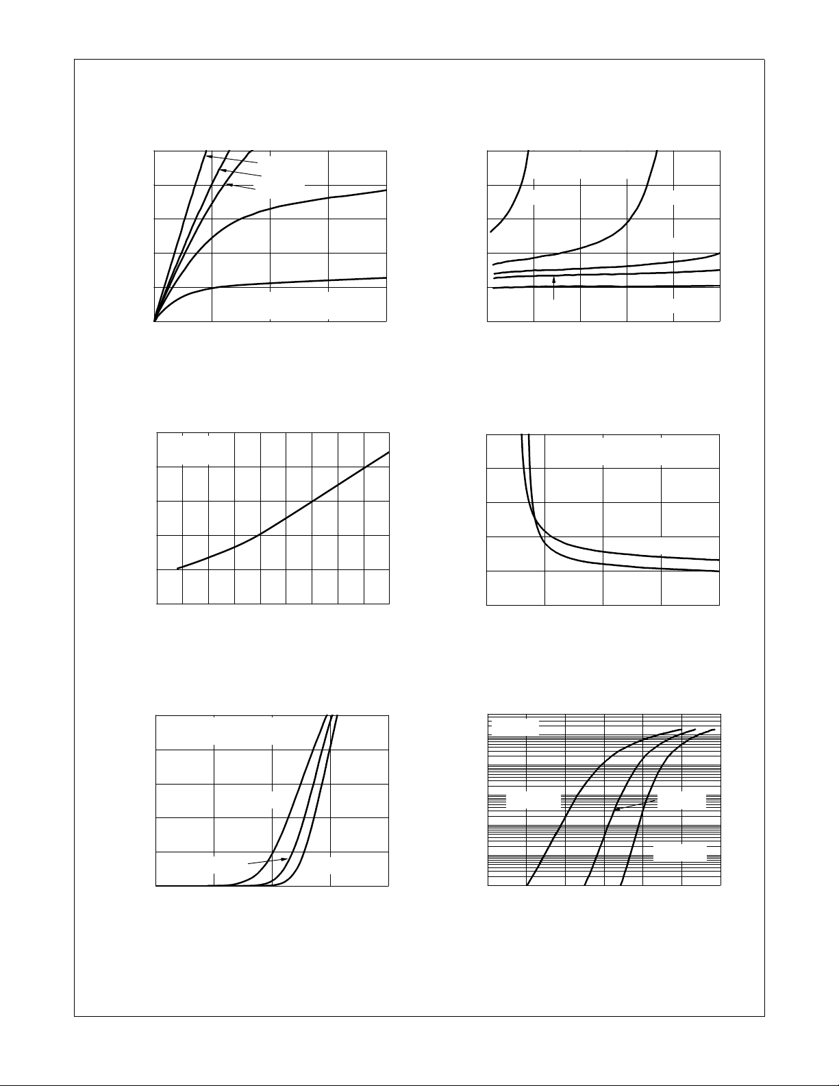
0.00.51.01.52.0
0
30
60
90
120
150
VGS = 3.5 V
VGS = 10 V
PULSE DURA TION = 80 μs
DUTY CYCLE = 0.5% MAX
VGS = 4 V
VGS = 5 V
VGS = 4.5 V
I
D
, DRAIN CURRENT (A)
V
DS
, DRAIN TO SOURCE VOLTAGE (V)
0306090120150
0
1
2
3
4
5
VGS = 3.5 V
PULSE DURATION = 80 μs
DUTY CYCLE = 0.5% MAX
NORMALIZED
DRAIN TO SOURCE ON-RESISTANCE
I
D
, DRAIN CURRENT (A)
V
GS
= 4 V
VGS = 4.5 V
VGS = 5 V
V
GS
= 10 V
-75 -50 -25 0 25 50 75 100 125 150
0.6
0.8
1.0
1.2
1.4
1.6
ID = 21 A
V
GS
= 10 V
NORMALIZED
DRAIN TO SOURCE ON-RESIST A NC E
T
J
, JUNCTION TEMPERATURE (
o
C)
246810
0
3
6
9
12
15
TJ = 125 oC
ID = 21 A
TJ = 25 oC
V
GS
, GATE TO S OURCE VOLTAGE (V)
r
DS(on)
,
DRAIN TO
SOURCE ON-RESISTANCE
(mΩ)
PULSE DURA TION = 80 μs
DUTY CYCLE = 0.5% MAX
12345
0
30
60
90
120
150
TJ = 150 oC
V
DS
= 5 V
PULSE DURATION = 80 μs
DUTY CYCLE = 0.5% MAX
TJ = -55 oC
TJ = 25 oC
I
D
, DRAIN CURRENT (A)
VGS, GATE TO SOURC E V OLTAGE (V)
0.0 0.2 0.4 0.6 0.8 1.0 1.2
0.001
0.01
0.1
1
10
100
TJ = -55 oC
TJ = 25 oC
TJ = 150 oC
V
GS
= 0 V
I
S
, REVERSE DRAIN CURRENT (A)
VSD, BODY DIODE FORWARD VOLTAGE (V)
500
Typical Characteristics T
Figure 1.
On Region Characteristics Figure 2.
= 25 °C unless otherwise noted
J
®
MOSFET
Nor m a l i z e d On-Resis t a n c e
vs Drain Current and Gate Voltage
Fi gure 3 . No r mali zed O n Res i sta n ce
vs Junction Temperature
©2012 Fairchild Semiconductor Corporation
FDMS7670 Rev.D2
Figure 5. Transfer Characteristics
Figure 4.
On-Re sistance v s Gate to
Source Voltage
Figure 6.
Sou rce to Drain Diode
Forward Voltage vs Source Current
3
www.fairchildsemi.com
Page 4

FDMS7670 N-Channel PowerTrench
0 10203040
0
2
4
6
8
10
ID = 21 A
VDD = 20 V
V
DD
= 10 V
V
GS
, GATE TO SOURCE VOLTAGE (V)
Qg, GATE CHARGE (nC)
VDD = 15 V
0.1 1 10
100
1000
50
f = 1 MHz
V
GS
= 0 V
CAPACITANCE (pF)
VDS, DRAIN TO SOURCE VOLTAGE (V)
C
rss
C
oss
C
iss
30
5000
0.01 0.1 1 10 100 1000
1
10
100
TJ = 100 oC
TJ = 25 oC
TJ = 125 oC
tAV, TIME IN AVALA NCHE (ms)
I
AS
, AVALANCHE CURRENT (A)
40
25 50 75 100 125 150
0
20
40
60
80
100
120
V
GS
= 4.5 V
Limited by Package
R
θJC
= 2.0 oC/W
V
GS
= 10 V
I
D
, DRAIN CURRENT (A)
T
C
, CASE TEMPERATURE (
o
C)
0.01 0.1 1 10 100
0.01
0.1
1
10
100
200
DERIVED FROM
TEST DATA
1 ms
1 s
10 ms
DC
10 s
100 ms
I
D
, DRAIN CURRENT (A)
VDS, DRAIN to SOURCE VOLTAGE (V)
THIS AREA IS
LIMITED BY r
DS(on)
SINGLE PULSE
T
J
= MAX RATED
R
θJA
= 125
o
C/W
T
A
= 25
o
C
10-410-310-210
-1
110
100 1000
0.5
1
10
100
1000
10000
SINGLE PULSE
R
θJA
= 125
o
C/W
T
A
= 25
o
C
VGS = 10 V
P(
PK
), PEAK TRANSIENT POWER (W)
t, PULSE WIDTH (sec)
Typical Characteristics T
Figure 7.
Gate Charge Characteristics Figure 8.
= 25 °C unless otherwise noted
J
®
MOSFET
Capacitance vs Drain
to Source Voltage
Figure 9.
Unc l a m p e d I ndu c t i v e
Switching Capability
©2012 Fairchild Semiconductor Corporation
FDMS7670 Rev.D2
Figure 11. Forward Bias Safe
Op
erating Area
Figure 10.
Ma xi mum Co nti nuous Drain
Current vs Case Temperature
Figure 12.
Single Pu ls e M aximum
Power Dissipation
4
www.fairchildsemi.com
Page 5

FDMS7670 N-Channel PowerTrench
10
-4
10
-3
10
-2
10
-1
110
100 1000
0.0005
0.001
0.01
0.1
1
2
SINGLE PULSE
R
θJA
= 125 oC/W
DUTY CYCLE-DESCENDING ORDER
NORMALIZED THERMAL
IMPEDANCE,
Z
θJA
t, RECTANGULAR PU L SE D U R ATION (sec)
D = 0.5
0.2
0.1
0.05
0.02
0.01
P
DM
t
1
t
2
NOTES:
DUTY FACTOR: D = t
1/t2
PEAK TJ = PDM x Z
θJA
x R
θJA
+ T
A
-120 -90 -60 -30 0 30 60
-5
0
5
10
15
20
25
di/dt = 300 A/μs
TIME (ns)
CURRENT (A)
0 30 60 90 120 150 180
-5
0
5
10
15
20
100
di/dt = 300 A/μs
TIME (ns)
CURRENT (A)
Typical Characteristics T
Figure 13.
= 25 °C unless otherwise noted
J
Junction-to-Ambient Transient Thermal Response Curve
Figure 15.
®
MOSFET
Figure 14.
Body Diode Reverse
Recovery Characteristics
©2012 Fairchild Semiconductor Corporation
FDMS7670 Rev.D2
5
www.fairchildsemi.com
Page 6

FDMS7670 N-Channel PowerTrench
Dimensional Outline and Pad Layout
®
MOSFET
©2012 Fairchild Semiconductor Corporation
FDMS7670 Rev.D2
6
www.fairchildsemi.com
Page 7

TRADEMARKS
tm
The following includes registered and unregistered trademarks and service marks, owned by Fairchild Semiconductor a nd/or its global subsid iaries, and is not
intended to be an exhaustive list of all such trademarks.
2Cool™
AccuPower™
AX-CAP™*
®
BitSiC
Build it Now™
CorePLUS™
CorePOWER™
CROSSVOLT™
CTL™
Current Transfer Logic™
DEUXPEED
Dual Cool™
EcoSPARK
EfficentMax™
ESBC™
Fairchild
Fairchild Semiconductor
FACT Quiet Series™
FACT
FAST
FastvCore™
FETBench™
FlashWriter
FPS™
®
®
®
®
®
®
*
®
F-PFS™
®
FRFET
Global Power Resource
Green Bridge™
Green FPS™
Green FPS™ e-Series™
Gmax™
GTO™
IntelliMAX™
ISOPLANAR™
Marking Small Speakers Sound Louder
and Better™
MegaBuck™
MICROCOUPLER™
MicroFET™
MicroPak™
MicroPak2™
MillerDrive™
MotionMax™
Motion-SPM™
mWSaver™
OptoHiT™
OPTOLOGIC
OPTOPLANAR
®
®
®
SM
PowerTrench
PowerXS™
Programmable Active Droop™
QFET
QS™
Quiet Series™
RapidConfigure™
Saving our world, 1mW/W/kW at a time™
SignalWise™
SmartMax™
SMART START™
Solutions for Your Success™
SPM
STEALTH™
SuperFET
SuperSOT™-3
SuperSOT™-6
SuperSOT™-8
SupreMOS
SyncFET™
Sync-Lock™
®
®
®
®
®
®*
The Power Franchise
TinyBoost™
TinyBuck™
TinyCalc™
®
TinyLogic
TINYOPTO™
TinyPower™
TinyPWM™
TinyWire™
®
TranSiC
TriFault Detect™
TRUECURRENT
μSerDes™
®
UHC
Ultra FRFET™
UniFET™
VCX™
VisualMax™
VoltagePlus™
XS™
®
®
®
*
*Trademarks of System General Corporation, used under license by Fairchild Semiconductor.
DISCLAIMER
FAIRCHILD SEMICONDUCTOR RESERVES THE RIGHT TO MAKE CHANGES WITHOUT FURTHER NOTICE TO ANY PRODUCTS HEREIN TO IMPROVE
RELIABILITY, FUNCTION, OR DESIGN. FAIRCHILD DOES NOT ASSUME ANY LIABILITY ARISING OUT OF THE APPLICATION OR USE OF ANY
PRODUCT OR CIRCUIT DESCRIBED HEREIN; NEITHER DOES IT CONVEY ANY LICENSE UNDER ITS PATENT RIGHTS, NOR THE RIGHTS OF OTHERS.
THESE SPECIFICATIONS DO NOT EXPAND THE TERMS OF FAIRCHILD’S WORLDWIDE TERMS AND CONDITIONS, SPECIFICALLY THE WARRANTY
THEREIN, WHICH COVERS THESE PRODUCTS.
FDMS7670 N-Channel PowerTrench
®
MOSFET
LIFE SUPPORT POLICY
FAIRCHILD’S PRODUCTS ARE NOT AUTHORIZED FOR USE AS CRITICAL COMPONENTS IN LIFE SUPPORT DEVICES OR SYSTEMS WITHOUT THE
EXPRESS WRITTEN APPROVAL OF FAIRCHILD SEMICONDUCTOR CORPORATION.
As used here in:
1. Life support devices or systems are devices or systems which, (a) are
intended for surgical implant into the body or (b) support or sustain life,
and (c) whose failure to perform when properly used in accordance with
instructions for use provided in the labeling, can be reasonably
expected to result in a significant injury of the user.
ANTI-COUNTERFEITING POLICY
Fairchild Semiconductor Corporation’s Anti-Counterfeiting Policy. Fairchild’s Anti-Counterfeiting Policy is also stated on our external website,
www.Fairchildsemi.com, under Sales Support
Counterfeiting of semiconductor parts is a growing problem in the industr y. All manufactures of semicondu ctor products are experiencing count erfeiting of their
parts. Customers who inadvertently purchase counterfeit parts experience ma ny problems such as lo ss of bran d reput ation, sub standard perf ormance, failed
application, and increased cost of production and manufacturing delays. Fairchild is taking strong measures to protect our selve s and our cu st omer s from the
proliferation of counterfeit parts. Fairchild stro ngly encourag es customers to purchase Fai rchild parts either directly from Fairchild or from Au thorized Fairchild
Distributors who are listed by country on our web page cited above. Products customers buy either from Fairchild directly or from Authorized Fairchild
Distributors are genuine parts, have full traceability, meet Fairchild’s quality standards for handing and storage and provide access to Fairchild’s full range of
up-to-date technical and product information. Fairchild and our Authorized Distributors will stand behind all warranties and will appropriately address and
warranty issues that may arise. Fairchild will not provide any warranty coverage or other assistance for parts bought from Unauthorized Sources. Fairchild is
.
2. A critical component in any component of a life support, device, or
system whose failure to perform can be reasonably expe cted to cause
the failure of the life support device or system, or to affect its safety or
effectiveness.
committed to combat this global problem and encourage our customers to do their part in stopping this practice by buying direct o r from authorized distr ibutors.
PRODUCT STATUS DEFINITIONS
Definition of Terms
Datasheet Identification Product Status Definition
Advance Information Formative / In Design
Preliminary First Production
No Identification Needed Full Production
Obsolete Not In Production
Datasheet contains the design specifications for product development. Specifications
may change in any manner without notice.
Datasheet contains preliminary data; supplementary data will be published at a later
date. Fairchild Semiconductor reserves the right to make changes at any time without
notice to improve design.
Datasheet contains final specifications. Fairchild Semiconductor reserves the right to
make changes at any time without notice to improve the design.
Datasheet contains specifications on a product that is discontinued by Fairchild
Semiconductor. The datasheet is for reference information only.
Rev. I61
©2012 Fairchild Semiconductor Corporation
FDMS7670 Rev.D2
7
www.fairchildsemi.com
 Loading...