

Page 1
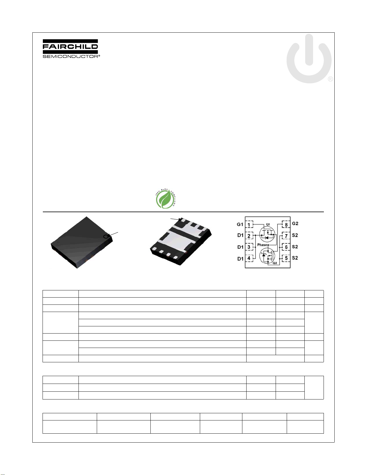
FDMS3624S
Power 56
G1
D1
D1
D1
G2
S2
S2
S2
D1
PHASE
(S1/D2)
Top Bottom
Pin 1
Pin 1
PowerTrench® Power Stage
25V Asymmetric Dual N-Channel MOSFET
FDMS3624S PowerTrench
December 2011
Features
Q1: N-Channel
Max r
Max r
Q2: N-Channel
Max r
Max r
Low inductance packaging shortens rise/fall times, resulting in
lower switching losses
MOSFET integration enables optimum layout for lower circuit
inductance and reduced switch node ringing
RoHS Compliant
= 5.0 mΩ at VGS = 10 V, ID = 17.5 A
DS(on)
= 5.7 mΩ at VGS = 4.5 V, ID = 16 A
DS(on)
= 1.8 mΩ at VGS = 10 V, ID = 30 A
DS(on)
= 2.2 mΩ at VGS = 4.5 V, ID = 27 A
DS(on)
General Description
This device includes two specialized N-Channel MOSFETs in a
dual PQFN package. The switch node has been internally
connected to enable easy placement and routing of synchronous
buck converters. The control MOSFET (Q1) and synchronous
SyncFET (Q2) have been designed to provide optimal power
efficiency.
Applications
Computing
Communications
General Purpose Point of Load
Notebook VCORE
®
Power Stage
MOSFET Maximum Ratings T
Symbol Parameter Q1 Q2 Units
V
DS
V
GS
I
D
E
AS
P
D
TJ, T
STG
Drain to Source Voltage 25 25 V
Gate to Source Voltage (Note 4) ±12 ±12 V
Drain Current -Continuous (Package limited) TC = 25 °C 30 60
-Pulsed 70 120
Single Pulse Avalanche Energy (Note 3) 29 86 mJ
Power Dissipation for Single Operation TA = 25 °C 2.2
Power Dissipation for Single Operation T
Operating and Storage Junction Temperature Range -55 to +150 °C
= 25 °C unless otherwise noted
A
= 25 °C 17.5
A
= 25 °C 1.0
A
1a
1a
1c
30
2.5
1.0
1b
1b
1d
A -Continuous T
W
Thermal Characteristics
R
θJA
θJA
R
θJC
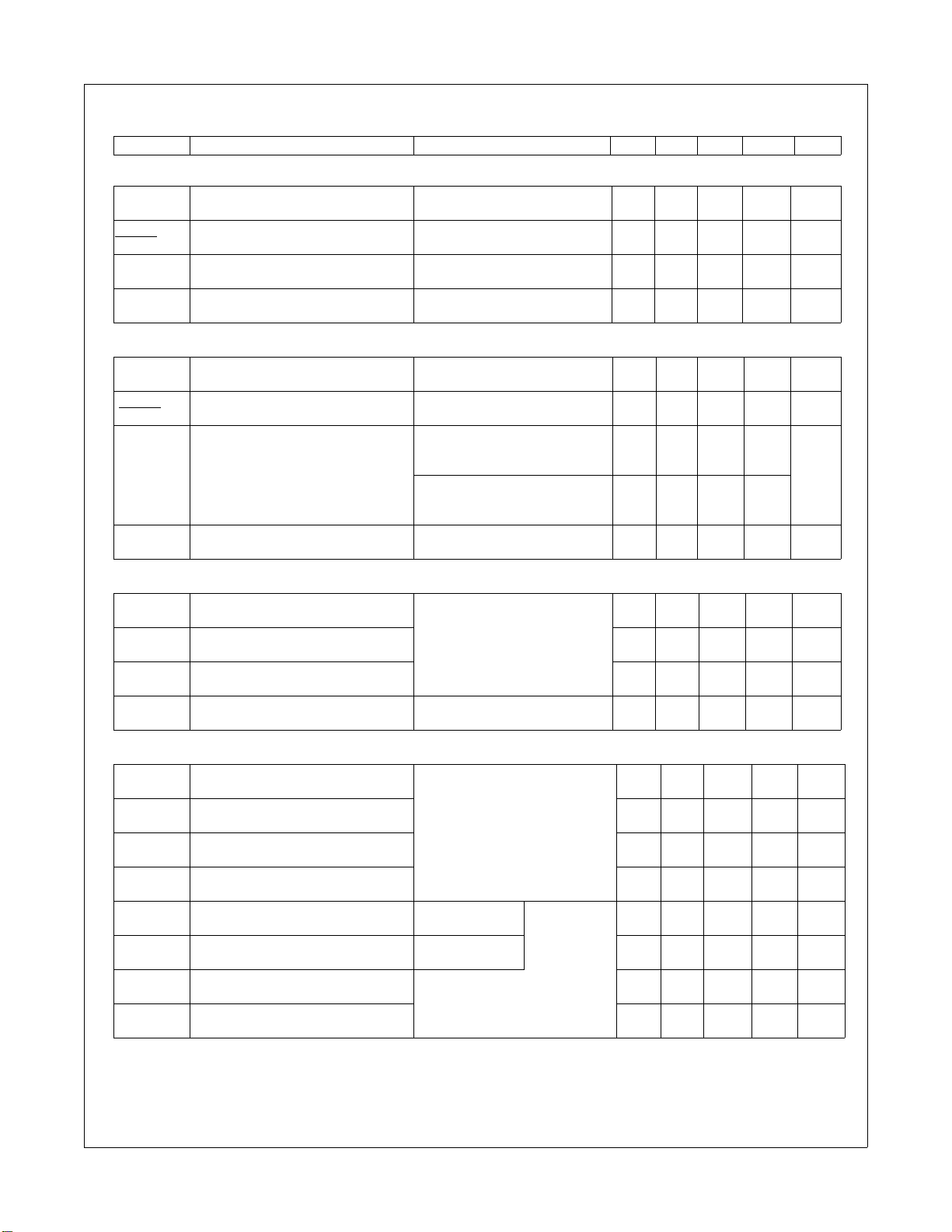
Package Marking and Ordering Information
Device Marking Device Package Reel Size Tape Width Quantity
©2011 Fairchild Semiconductor Corporation 1 www.fairchildsemi.com
FDMS3624S Rev.C2
Thermal Resistance, Junction to Ambient 57
Thermal Resistance, Junction to Ambient 125
Thermal Resistance, Junction to Case 3.0 2.2
08OD
07OD
FDMS3624S Power 56 13 ” 12 mm 3000 units
1a
1c
50
120
1b
1d
°C/WR
Page 2
FDMS3624S PowerTrench
Electrical Characteristics T
= 25 °C unless otherwise noted
J
Symbol Parameter Test Conditions Type Min Typ Max Units
Off Characteristics
BV
ΔBV
ΔT
I
DSS
I
GSS
DSS
DSS
J
= 250 μA, VGS = 0 V
Drain to Source Breakdown Voltage
Breakdown Voltage Temperature
Coefficient
Zero Gate Voltage Drain Current VDS = 20 V, V
D
I
= 1 mA, VGS = 0 V
D
ID = 250 μA, referenced to 25 °C
I
= 10 mA, referenced to 25 °C
D
= 0 V
GS
Gate to Source Leakage Current VGS = 12 V/-8 V, VDS= 0 V
Q1Q225
25
Q1
Q2
Q1
Q2
Q1
Q2
V
12
24
500
±100
±100nAnA
mV/°C
1
I
On Characteristics
V
V
GS(th)
ΔV
ΔT
r
DS(on)
g
FS
GS(th)
J
Gate to Source Threshold Voltage
Gate to Source Threshold Voltage
Temperature Coefficient
Drain to Source On Resistance
Forward Transconductance
= VDS, ID = 250 μA
GS
V
= VDS, ID = 1 mA
GS
ID = 250 μA, referenced to 25 °C
I
= 10 mA, referenced to 25 °C
D
= 10 V, ID = 17.5 A
V
GS
V
= 4.5 V, ID = 16 A
GS
V
= 10 V , ID = 17.5 A,TJ =125 °C
GS
V
= 10 V, ID = 30 A
GS
V
= 4.5 V, ID = 27 A
GS
V
= 10 V, ID =30 A ,TJ =125 °C
GS
V
= 5 V, ID = 17.5 A
DS
V
= 5 V, ID = 30 A
DS
Q1Q20.8
1.1
Q1
Q2
Q1
Q2
Q1
Q2
1.2
1.4
-4
-3
3.8
4.4
5.4
1.5
1.8
2.1
100
240
2.0
2.2
mV/°C
5.0
5.7
7.0
1.8
2.2
2.7
μA
μA
V
mΩ
S
®
Power Stage
Dynamic Characteristics
C
iss
C
oss
C
rss
R
g
Input Capacitance
Output Capacitance
Reverse Transfer Capacitance
Gate Resistance
Switching Characteristics
t
d(on)
t
r
t
d(off)
t
f
Q
Q
Q
Q
g
g
gs
gd
Turn-On Delay Time
Rise Time
Turn-Off Delay Time
Fall Time
Total Gate Charge V
Total Gate Charge V
Gate to Source Gate Charge
Gate to Drain “Miller” Charge
Q1:
= 13 V, VGS = 0 V, f = 1 MHZ
V
DS
Q2:
= 13 V, VGS = 0 V, f = 1 MHZ
V
DS
Q1
Q2
Q1
Q2
Q1
Q2
Q1
Q2
1570
4045
448
946
61
117
0.4
0.9
pF
pF
pF
Ω
7
11
2
5
23
39
2
4
26
59
12
27
3.3
8.2
2.7
7.6
ns
ns
ns
ns
nC
nC
nC
nC
Q1:
= 13 V , ID = 17.5 A, R
V
DD
Q2:
= 13 V, ID = 30A, R
V
DD
= 0 V to 10 V
GS
= 0 V to 4.5 V
GS
= 6 Ω
GEN
= 6 Ω
GEN
Q1
V
= 13 V,
DD
I
= 17.5 A
D
Q2
VDD = 13 V,
I
= 30 A
D
Q1
Q2
Q1
Q2
Q1
Q2
Q1
Q2
Q1
Q2
Q1
Q2
Q1
Q2
Q1
Q2
©2011 Fairchild Semiconductor Corporation 2 www.fairchildsemi.com
FDMS3624S Rev.C2
Page 3
FDMS3624S PowerTrench
Electrical Characteristics T
= 25 °C unless otherwise noted
J
Symbol Parameter Test Conditions Type Min Typ Max Units
Drain-Source Diode Characteristics
0.8
0.8
23
28
28
1.2
1.2
9
is determined by
θCA
V
= 0 V, IS = 17.5 A (Note 2)
V
SD
t
rr
Q
rr
Notes:
1.R
is determined with the device mo un ted on a 1 in2 pad 2 oz copper pad on a 1.5 x 1.5 in. boar d o f FR - 4 mat er i al. R
θJA
the user's board design.
Source to Drain Diode Forward Voltage
Reverse Recovery Time
Reverse Recovery Charge
a. 57 °C/W when mounted on
a 1 in2 pad of 2 oz copper
SF
SS
DS
DF
G
c. 125 °C/W when mounted on a
minimum pad of 2 oz copper
GS
V
= 0 V, IS = 30 A (Note 2)Q1Q2
GS
Q1
= 17.5 A, di/dt = 100 A/μs
I
F
Q2
I
= 30 A, di/dt = 300 A/μs
F
G
DF
DS
Q1
Q2
Q1
Q2
is guaranteed by design while R
θJC
b. 50 °C/W when mounted on
a 1 in
SS
SF
d. 120 °C/W when mounted on a
minimum pad of 2 oz copper
2
pad of 2 oz copper
ns
nC
V
®
Power Stage
SF
SS
DS
DF
G
2 Pulse Test: Pulse Width < 300 μs, Duty cycle < 2.0%.
of 29 mJ is based on starting TJ = 25 oC; N-ch: L = 1.2 mH, IAS = 7 A, VDD = 23 V, VGS = 10 V. 100% test at L = 0.1 mH, IAS = 16 A.
3. Q1 :E
AS
Q2: EAS of 86 mJ is based on starting TJ = 25 oC; N-ch: L = 0.6 mH, IAS = 17 A, VDD = 23 V, VGS = 10 V. 100% test at L = 0.1 mH, IAS = 31 A.
4. As an N-ch device, the negative Vgs rating is for low duty cycle pulse occurrence only. No continuous rating is implied.
G
SS
SF
DS
DF
©2011 Fairchild Semiconductor Corporation 3 www.fairchildsemi.com
FDMS3624S Rev.C2
Page 4
FDMS3624S PowerTrench
0.0 0 .3 0.6 0.9 1.2 1.5
0
10
20
30
40
50
60
70
V
GS
= 2.5 V
V
GS
= 3 V
V
GS
= 10 V
V
GS
= 4.5 V
V
GS
= 3.5 V
PULSE DURATION = 80 μs
DUTY CYCLE = 0.5% MAX
I
D
, DRAIN CURRENT (A)
V
DS
, DRAIN TO SOURCE VOLTAGE (V)
0 10203040506070
0.5
1.0
1.5
2.0
2.5
3.0
VGS = 2.5 V
VGS = 4.5 V
VGS = 3 V
PULSE DURATION = 80 μs
DUTY CYCLE = 0.5% MAX
NORMALIZED
DRAIN TO SOURCE ON-RESISTANCE
I
D
, DRAIN CURRENT (A)
VGS = 3.5 V
V
GS
= 10 V
-75 -50 -25 0 25 50 75 100 125 150
0.6
0.8
1.0
1.2
1.4
1.6
1.8
ID = 17.5 A
V
GS
= 10 V
NORMALIZED
DRAIN TO SOURCE ON-RESISTANC E
T
J
, JUNCTION TEMPERATURE (
o
C)
2345678910
0
4
8
12
16
20
TJ = 125 oC
ID = 17.5 A
TJ = 25 oC
V
GS
, GATE TO SOURCE VOLTA G E (V)
r
DS(on)
,
DRAIN TO
SOURCE ON-RESISTANCE
(mΩ)
PULSE DURATION = 80 μs
DUTY CYCLE = 0.5% MAX
0.5 1.0 1.5 2.0 2.5 3.0
0
10
20
30
40
50
60
70
TJ = 150 oC
V
DS
= 5 V
PULSE DURATION = 80 μs
DUTY CYCLE = 0.5% MAX
TJ = -55 oC
TJ = 25 oC
I
D
, DRAIN CURRENT (A)
VGS, GATE TO SOURCE VOLTAGE (V)
0.0 0.2 0.4 0.6 0.8 1.0 1.2
0.001
0.01
0.1
1
10
70
TJ = -55 oC
TJ = 25 oC
TJ = 150 oC
V
GS
= 0 V
I
S
, REVERSE DRAIN CURRENT (A)
VSD, BODY DIODE FORWARD VOLTAGE (V)
Typical Characteristics (Q1 N-Channel) T
Figure 1.
On Region Characteristics Figure 2.
= 25°C unless otherwise noted
J
Norma l i z ed On-Res i s t ance
vs Drain Current and Gate Voltage
®
Power Stage
Fig ure 3 . Norm aliz ed On Resis tanc e
vs Junction Temperature
©2011 Fairchild Semiconductor Corporation 4 www.fairchildsemi.com
FDMS3624S Rev.C2
Figure 5. Transfer Characteristics
Figure 4.
On-Resistanc e v s Gate to
Source Voltage
Figure 6.
Source to Dr ain Diode
Forward Voltage vs Source Current
Page 5

FDMS3624S PowerTrench
0 4 8 12 16 20 24 28
0
2
4
6
8
10
ID = 17.5 A
V
DD
= 15 V
V
DD
= 10 V
V
GS
, GATE TO SOURCE VOLTAGE (V)
Qg, GATE CHARGE (nC)
VDD = 13 V
0.1 1 10 30
10
100
1000
2000
f = 1 MHz
V
GS
= 0 V
CAPACITANCE (pF)
VDS, DRAIN TO SOURCE VOLTAGE (V)
C
rss
C
oss
C
iss
0.001 0.01 0.1 1 10 50
1
10
50
TJ = 100 oC
TJ = 25 oC
TJ = 125 oC
tAV, TIME IN AVALANCHE (ms)
I
AS
, AVALANCHE CURRENT (A)
25 50 75 100 125 150
0
10
20
30
40
50
60
70
80
R
θJC
= 3.0 oC/W
V
GS
= 4.5 V
Limited by Package
V
GS
= 10 V
I
D
, DRAIN CURRENT (A)
T
C
, CASE TEMPERATURE (
o
C)
0.01 0.1 1 10 100200
0.01
0.1
1
10
100
100 μs
DC
100 ms
10 ms
1 ms
1s
I
D
, DRAIN CURRENT (A)
VDS, DRAIN to SOURCE VOLTAGE (V)
THIS AREA IS
LIMITED BY r
DS(on)
SINGLE PULSE
T
J
= MAX RATED
R
θJA
= 125
o
C/W
T
A
= 25
o
C
10s
10-410-310-210
-1
110
100 1000
0.5
1
10
100
1000
SINGLE PULSE
R
θJA
= 125 oC/W
P(
PK
), PEAK TRANSIENT POWER (W)
t, PULSE WIDTH (sec)
Typical Characteristics (Q1 N-Channel) T
Figure 7.
Gate Charge Characteristics Figure 8.
= 25°C unless otherwise noted
J
Capacitance v s D r a i n
to Source Voltage
®
Power Stage
Figure 9.
Uncla m p e d I n d u c t i v e
Switching Capability
©2011 Fairchild Semiconductor Corporation 5 www.fairchildsemi.com
FDMS3624S Rev.C2
Figure 11. Forward Bias Safe
Op
erating Area
Figure 10.
Ma xim um Continuou s Dr ain
Current vs Case Temperature
Figure 12.
Si ngle Pul se Max imum
Power Dissipation
Page 6

FDMS3624S PowerTrench
10
-4
10
-3
10
-2
10
-1
110
100 1000
0.001
0.01
0.1
1
2
SINGLE PULSE
R
θJA
= 125 oC/W
(Note 1b)
DUTY CYCLE-DESCENDING ORDER
NORMALIZED THERMAL
IMPEDANCE,
Z
θJA
t, RECTANGULAR PU L SE DURATION (sec)
D = 0.5
0.2
0.1
0.05
0.02
0.01
P
DM
t
1
t
2
NOTES:
DUTY FACTOR: D = t1/t
2
PEAK TJ = PDM x Z
θJA
x R
θJA
+ T
A
Typical Characteristics (Q1 N-Channel) T
Figure 13.
Junction-to-Ambient Transient Thermal Response Curve
= 25°C unless otherwise noted
J
®
Power Stage
©2011 Fairchild Semiconductor Corporation 6 www.fairchildsemi.com
FDMS3624S Rev.C2
Page 7

FDMS3624S PowerTrench
0.0 0.3 0.6 0.9 1.2 1.5
0
20
40
60
80
100
120
V
GS
= 2.5 V
V
GS
= 3 V
V
GS
= 10 V
V
GS
= 4.5 V
V
GS
= 3.5 V
PULSE DURATION = 80 μs
DUTY CYCLE = 0.5% MAX
I
D
, DRAIN CURRENT (A)
V
DS
, DRAIN TO SOURCE VOLTAGE (V)
0 20406080100120
0
1
2
3
4
VGS = 2.5 V
VGS = 3.5 V
PULSE DURA TION = 80 μs
DUTY CYCLE = 0.5% MAX
NORMALIZED
DRAIN TO SOURCE ON-RESISTANCE
I
D
, DRAIN CURRENT (A)
V
GS
= 3 V
VGS = 4.5 V
V
GS
= 10 V
-75 -50 -25 0 25 50 75 100 125 150
0.6
0.8
1.0
1.2
1.4
1.6
ID = 30 A
V
GS
= 10 V
NORMALIZED
DRAIN TO SOURCE ON-RESISTANCE
T
J
, JUNCTION TEMPERATURE (
o
C)
246810
0
1
2
3
4
5
6
7
TJ = 125 oC
ID = 30 A
TJ = 25 oC
V
GS
, GATE TO SOURCE VOLTA G E (V)
r
DS(on)
,
DRAIN TO
SOURCE ON-RESISTANCE
(mΩ)
PULSE DURATION = 80 μs
DUTY CYCLE = 0.5% MAX
1.0 1.5 2.0 2.5 3.0
0
20
40
60
80
100
120
TJ = 125 oC
V
DS
= 5 V
PULSE DURATION = 80 μs
DUTY CYCLE = 0.5% MAX
TJ = -55 oC
TJ = 25 oC
I
D
, DRAIN CURRENT (A)
VGS, GATE TO SOURCE VOLTAGE (V)
0.0 0.2 0.4 0.6 0.8 1.0
0.001
0.01
0.1
1
10
100
200
TJ = -55 oC
TJ = 25 oC
TJ = 125 oC
V
GS
= 0 V
I
S
, REVERSE DRAIN CURRENT (A)
VSD, BODY DIODE FORWARD VOLTAGE (V)
Typical Characteristics (Q2 N-Channel) T
Figure 14.
On-Region Characteristics Figure 15. Normalized on-Resistance vs Drain
= 25 °C unless otherwise noted
J
Current and Gate Voltage
®
Power Stage
Figure 16. Normalized On-Resistance
vs Junction Temperature
©2011 Fairchild Semiconductor Corporation 7 www.fairchildsemi.com
FDMS3624S Rev.C2
Figure 18. Transfer Characteristics Figure 19. Source to Drain Diode
Figure 17. On-Resistance vs Gate to
Source Voltage
Forward Voltage vs Source Current
Page 8

FDMS3624S PowerTrench
0 102030405060
0
2
4
6
8
10
ID = 30 A
V
DD
= 15 V
V
DD
= 10 V
V
GS
, GATE TO SOURCE VOLTAGE (V)
Qg, GATE CHARGE (nC)
VDD = 13 V
0.1 1 10 30
10
100
1000
10000
f = 1 MH z
V
GS
= 0 V
CAPACITANCE (pF)
VDS, DRAIN TO SOURCE VOLTAGE (V)
C
rss
C
oss
C
iss
0.001 0.01 0.1 1 10 100 1000
1
10
100
TJ = 100 oC
TJ = 25 oC
TJ = 125 oC
tAV, TIME IN AVALANCHE (ms)
I
AS
, AVALANCHE CURRENT (A)
25 50 75 100 125 150
0
30
60
90
120
150
R
θJC
= 2.2 oC/W
V
GS
= 4.5 V
Limited by Package
V
GS
= 10 V
I
D
, DRAIN CURRENT (A)
T
C
, CASE TEMPERATURE (
o
C)
0.01 0.1 1 10 100
0.01
0.1
1
10
100
200
100 μs
DC
100 ms
10 ms
1 ms
1s
I
D
, DRAIN CURRENT (A)
VDS, DRAIN to SOURCE VOLTAGE (V)
THIS AREA IS
LIMITED BY r
DS(on)
SINGLE PULSE
T
J
= MAX RATED
R
θJA
= 120
o
C/W
T
A
= 25
o
C
10s
10-410-310-210
-1
110
100 1000
0.5
1
10
100
1000
3000
SINGLE PULSE
R
θJA
= 120 oC/W
P(
PK
), PEAK TRANSIENT POWER (W)
t, PULSE WIDTH (sec)
Typical Characteristics (Q2 N-Channel) T
Figure 20. Gate Charge Characteristics
= 25°C unless otherwise noted
J
Figure 21. Capacitance vs Drain
to Source Voltage
®
Power Stage
Figure 22. Unclamped Inductive
Switching Capability
©2011 Fairchild Semiconductor Corporation 8 www.fairchildsemi.com
FDMS3624S Rev.C2
Fi gure 24. Fo rward Bi as Safe
Operating Area
Figu r e 23. M a ximum C o ntinu o us Dra i n
Current vs Case Temperature
Figure 25. Single Pulse Maximum Power
Dissipation
Page 9

10
-4
10
-3
10
-2
10
-1
110
100 1000
0.0001
0.001
0.01
0.1
1
2
SINGLE PULSE
R
θJA
= 120 oC/W
(Note 1b)
DUTY CYCLE-DESCENDING ORDER
NORMALIZED THERMAL
IMPEDANCE,
Z
θJA
t, RECTANGULAR PULSE DURATION (sec)
D = 0.5
0.2
0.1
0.05
0.02
0.01
P
DM
t
1
t
2
NOTES:
DUTY FACTOR: D = t
1/t2
PEAK TJ = PDM x Z
θJA
x R
θJA
+ T
A
FDMS3624S PowerTrench
Typical Characteristics (Q2 N-Channel) T
Figure 26. Junction-to-Ambient Transient Thermal Response Curve
= 25 °C unless otherwise noted
J
®
Power Stage
©2011 Fairchild Semiconductor Corporation 9 www.fairchildsemi.com
FDMS3624S Rev.C2
Page 10

0 40 80 120 160 200 240 280 320 360
-5
0
5
10
15
20
25
30
35
CURRENT (A)
TIME (ns)
di/dt = 300 A/μs
0 5 10 15 20 25
10
-6
10
-5
10
-4
10
-3
10
-2
TJ = 125 oC
TJ = 100 oC
TJ = 25 oC
I
DSS
, REVERSE LEAKAGE CURRENT (A)
VDS, REVERSE VOLTAGE (V)
Typical Characteristics (continued)
SyncFET Schottky body diode
Characteristics
FDMS3624S PowerTrench
Fairchild’s SyncFET process embeds a Schottky diode in parallel
with PowerTrench MOSFET. This diode exhibits similar
characteristics to a discrete external Schottky diode in parallel
with a MOSFET. Figure 27 shows the reverse recovery
characteristic of the FDMS3624S.
Figure 27. FDMS3624S SyncFET body
diode reverse recovery characteristic
Schottky barrier diodes exhibit significant leakage at high temperature and high reverse voltage. This will increase the power
in the device.
Figure 28. SyncFET body diode reverse
leakage versus drain-source voltage
®
Power Stage
©2011 Fairchild Semiconductor Corporation 10 www.fairchildsemi.com
FDMS3624S Rev.C2
Page 11

Dimensional Outline and Pad Layout
C
L
L
CPKG
PKG
5.10
4.90
6.10
5.90
C
3.00
2.80
3.81
1.02
0.82
TOP VIEW
SIDE VIEW
BOTTOM VIEW
14
85
123
4
876
0.10 CAB
0.05
C
2.25
2.05
5
0.58
0.38
NOTES : UNLES S OTHERWISE SPECIFIE D
A) DOES NOT FULLY CO NFORM TO
JEDE C REGIS TRATI ON, MO-240,
ISSUE B DATED 10/2009.
B) ALL DIMENSIONS ARE IN
MILLIMETERS.
C) DIME NSIONS DO NO T INCLUDE
BURRS OR MOLD FLASH. MOLD
FLASH OR BURRS DOES NOT
EXCEED 0.10MM.
D) DIME NSI ONING AND TOLERANCI NG
PER ASME Y14.5M-1994.
E) IT IS RECOMMENDED TO HAVE NO
TRACES OR VIAS WITHIN THE KEEP
OUT AREA.
F) DRAWING FI L E NAME: PQN08EREV4.
SEE
DETAIL A
DETAIL A
(SCALE: 2X)
0.05
0.00
0.30
0.20
0.08
C
PIN #1
IDE N T M A Y
APPEAR AS
OPT IONAL
SEA TING
PLANE
0.10 C
1.10
0.90
RE C O M ME N DED LA ND P A TTE R N
0.65 TYP
1
2
3
4
5
6 7 8
1.27
1.32
1.12
A
0.10
C
2X
B
0.10 C
2X
0.00
0.00
1.60
2.52
1.21
2.31
1.18
1. 2 7 TY P
2.00
2.15
0.63
0.63
0.59
3.18
4.00
C
L
C
L
0.51
0.31
0.58
0.38
2.13
3.15
0.35
0.70
0.50
3.90
3.70
0.44
0.24
6X
0.71
0.61
KEEP
OUT
AREA
5.10
4.16
©2011 Fairchild Semiconductor Corporation 11 www.fairchildsemi.com
FDMS3624S Rev.C2
FDMS3624S PowerTrench
®
Power Stage
Page 12

TRADEMARKS
tm
®
™
tm
tm
The following includes registered and unregistered trademar ks and service marks, owned by Fair child Semicondu ctor and/or its glo bal subsidiaries, and is no t
intended to be an exhaustive list of all such trademarks.
2Cool™
AccuPower™
Auto-SPM™
AX-CAP™*
®
BitSiC
Build it Now™
CorePLUS™
CorePOWER™
CROSSVOLT™
CTL™
Current Transfer Logic™
DEUXPEED
Dual Cool™
EcoSPARK
EfficentMax™
®
®
ESBC™
®
Fairchild
Fairchild Semiconductor
FACT Quiet Series™
®
FACT
®
FAST
FastvCore™
FETBench™
FlashWriter
®
*
®
FPS™
F-PFS™
®
FRFET
Global Power Resource
GreenBridge™
Green FPS™
Green FPS™ e-Series™
Gmax™
GTO™
IntelliMAX™
ISOPLANAR™
Marking Small Speakers Sound Louder
and Better™
MegaBuck™
MICROCOUPLER™
MicroFET™
MicroPak™
MicroPak2™
MillerDrive™
MotionMax™
Motion-SPM™
mWSaver™
OptoHiT™
OPTOLOGIC
OPTOPLANAR
®
®
SM
®
PowerTrench
PowerXS™
Programmable Active Droop™
QFET
QS™
Quiet Series™
RapidConfigure™
®
®
Saving our world, 1mW/W/kW at a time™
SignalWise™
SmartMax™
SMART START™
Solutions for Your Success™
®
SPM
STEALTH™
SuperFET
SuperSOT™-3
SuperSOT™-6
SuperSOT™-8
SupreMOS
SyncFET™
Sync-Lock™
®
®
®*
The Power Franchise
TinyBoost™
TinyBuck™
TinyCalc™
TinyLogic
TINYOPTO™
TinyPower™
TinyPWM™
TinyWire™
TranSiC
TriFault Detect™
TRUECURRENT
μSerDes™
UHC
Ultra FRFET™
UniFET™
VCX™
VisualMax™
VoltagePlus™
XS™
®
®
®
®
®
®
*
FDMS3624S PowerTrench
®
Power Stage
*Trademarks of System General Corporation, used under license by Fairchild Semiconductor.
DISCLAIMER
FAIRCHILD SEMICONDUCTOR RESERVES THE RIGHT TO MAKE CHANGES WITHOUT FURTHER NOTICE TO ANY PRODUCTS HEREIN TO IMPROVE
RELIABILITY, FUNCTION, OR DESIGN. FAIRCHILD DOES NOT ASSUME ANY LIABILITY ARISING OUT OF THE APPLICATION OR USE OF ANY
PRODUCT OR CIRCUIT DESCRIBED HEREIN; NEITHER DOES IT CONVEY ANY LICENSE UNDER ITS PATENT RIGHTS, NOR THE RIGHTS OF OTHERS.
THESE SPECIFICATIONS DO NOT EXPAND THE TERMS OF FAIRCHILD’S WORLDWIDE TERMS AND CONDITIONS, SPECIFICALLY THE WARRANTY
THEREIN, WHICH COVERS THESE PRODUCTS.
LIFE SUPPORT POLICY
FAIRCHILD’S PRODUCTS ARE NOT AUTHORIZED FOR USE AS CRITICAL COMPONENTS IN LIFE SUPPORT DEVICES OR SYSTEMS WITHOUT THE
EXPRESS WRITTEN APPROVAL OF FAIRCHILD SEMICONDUCTOR CORPORATION.
As used here in:
1. Life support devices or systems are devices or systems which, (a) are
intended for surgical implant into the body or (b) support or sustain life,
and (c) whose failure to perform when properly used in accordance with
instructions for use provided in the labeling, can be reasonably
expected to result in a significant injury of the user.
ANTI-COUNTERFEITING POLICY
Fairchild Semiconductor Corporation’s Anti-Counterfeiting Policy. Fairchild’s Anti-Counterfeiting Policy is also stated on our external website,
www.Fairchildsemi.com, under Sales Support
Counterfeiting of semiconductor parts is a growing proble m in the industry. All manufactures of semicondu ctor products a re experiencing counterfe iting of their
parts. Customers who inadvertently purchase counterfeit parts experience many problems su ch as l oss of bra nd reput ation , su bstan dard per fo rmance, f ailed
application, and increased cost of production and manufacturing delays. Fairchild is taking st rong measures to protect ourselves and our customers from the
proliferation of counterfeit parts. Fairchild stro ngly encourages custo mers to purchase Fairchild parts eithe r directly fro m Fairchild or from A uthorized Fairchil d
Distributors who are listed by country on our web page cited above. Products customers buy either from Fairchild directly or from Authorized Fairchild
Distributors are genuine parts, have full traceabi lity, meet Fairchild’s quality standards for handing and storage and provide access to Fairchild’s full range of
up-to-date technical and product information. Fairchild and our Authorized Distributors will stand behind all warranties and will appropriately address and
warranty issues that may arise. Fairchild will not provide any warranty coverage or other assistance for parts bought from Unauthorized Sources. Fairchild is
.
2. A critical component in any component of a life support, device, or
system whose failure to perform can be reasonably expected to cause
the failure of the life support device or system, or to affect its safety or
effectiveness.
committed to combat this global problem and encourage our customers to do their part in stopping th is practice by buying direct or from authorized distribut ors.
PRODUCT STATUS DEFINITIONS
Definition of Terms
Datasheet Identification Product Status Definition
Advance Information Formative / In Design
Preliminary First Production
No Identification Needed Full Production
Obsolete Not In Production
Datasheet contains the design specifications for product development. Specifications
may change in any manner without notice.
Datasheet contains preliminary data; supplementary data will be published at a later
date. Fairchild Semiconductor reserves the right to make changes at any time without
notice to improve design.
Datasheet contains final specifications. Fairchild Semiconductor reserves the right to
make changes at any time without notice to improve the design.
Datasheet contains specifications on a product that is discontinued by Fairchild
Semiconductor. The datasheet is for reference information only.
Rev. I60
©2011 Fairchild Semiconductor Corporation 12 www.fairchildsemi.com
FDMS3624S Rev.C2
 Loading...