

Page 1
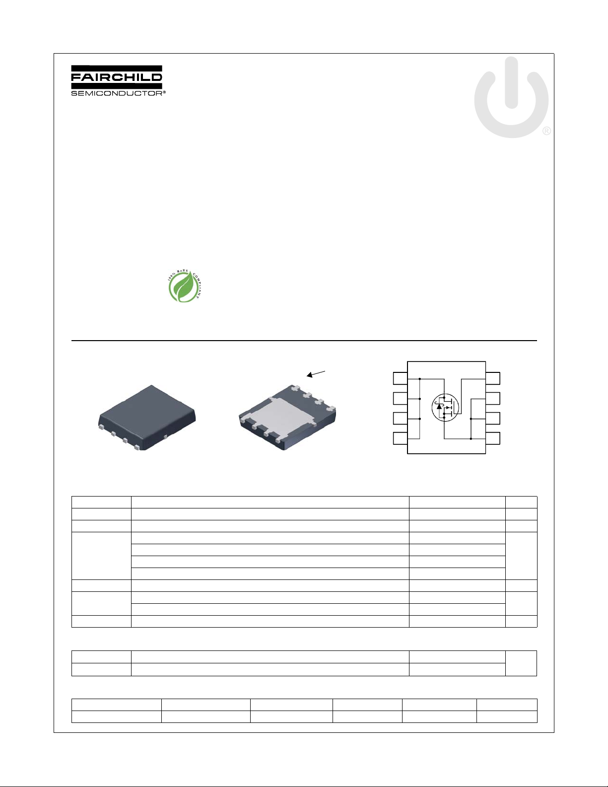
FDMS0312S
N-Channel PowerTrench® SyncFETTM
30 V, 42 A, 4.9 m:
FDMS0312S N-Channel PowerTrench
July 2011
Features
Max r
Max r
Advanced Package and Silicon combination for low r
and high efficiency
SyncFET Schottky Body Diode
MSL1 robust package design
100% UIL tested
RoHS Compliant
= 4.9 m: at V
DS(on)
= 5.8 m: at VGS = 4.5 V, ID = 14 A
DS(on)
Top
= 10 V, ID = 18 A
GS
Power 56
D
D
D
D
DS(on)
Bottom
General Description
The FDMS0312S has been designed to minimize losses in
power conversion application. Advancements in both silicon and
package technologies have been combined to offer the lowest
r
while maintaining excellent switching performance. This
DS(on)
device has the added benefit of an efficient monolithic Schottky
body diode.
Applications
Synchronous Rectifier for DC/DC Converters
Notebook Vcore/ GPU low side switch
Networking Point of Load low side switch
Desktop
Pin 1
S
S
S
G
D
5
D
6
D
7
D
8
G
4
S
3
S
2
S
1
®
SyncFET
TM
MOSFET Maximum Ratings T
Symbol Parameter Ratings Units
V
DS
V
GS
I
D
E
AS
P
D
, T
T
J
STG
Thermal Characteristics
R
TJC
R
TJA
Package Marking and Ordering Information
Device Marking Device Package Reel Size Tape Width Quantity
FDMS0312S FDMS0312S Power 56 3 ’’ 12 mm 3000 units
©2011 Fairchild Semiconductor Corporation
FDMS0312S Rev.D
Drain to Source Voltage 30 V
Gate to Source Voltage (Note 4) ±20 V
Drain Current -Continuous (Package limited) TC= 25 °C 42
-Continuous (Silicon limited) T
-Continuous T
-Pulsed 90
Single Pulse Avalanche Energy (Note 3) 60 mJ
Power Dissipation TC = 25 °C 46
Power Dissipation T
Operating and Storage Junction Temperature Range -55 to +150 °C
Thermal Resistance, Junction to Case 2.7
Thermal Resistance, Junction to Ambient (Note 1a) 50
= 25 °C unless otherwise noted
A
= 25 °C 83
C
= 25 °C (Note 1a) 19
A
= 25 °C (Note 1a) 2.5
A
1
A
W
°C/W
www.fairchildsemi.com
Page 2
FDMS0312S N-Channel PowerTrench
Electrical Characteristics T
= 25 °C unless otherwise noted
J
Symbol Parameter Test Conditions Min Typ Max Units
Off Characteristics
BV
DSS
'BV
DSS
'T
J
I
DSS
I
GSS
On Characteristics
V
GS(th)
'V
GS(th)
'T
J
r
DS(on)
g
FS
Drain to Source Breakdown Voltage ID = 1 mA, VGS = 0 V 30 V
Breakdown Voltage Temperature
Coefficient
Zero Gate Voltage Drain Current VDS = 24 V, V
Gate to Source Leakage Current, Forward VGS = 20 V, V
(Note 2)
I
= 10 mA, referenced to 25 °C 18 mV/°C
D
= 0 V 500 PA
GS
= 0 V 100 nA
DS
Gate to Source Threshold Voltage VGS = VDS, ID = 1 mA 1.2 1.9 3.0 V
Gate to Source Threshold Voltage
Temperature Coefficient
Static Drain to Source On Resistance
I
= 10 mA, referenced to 25 °C -5 mV/°C
D
V
= 10 V, I
GS
= 4.5 V, ID = 14 A 4.7 5.8
GS
= 10 V, ID = 18 A, TJ= 125 °C 5 6.2
V
GS
= 18 A 3.6 4.9
D
Forward Transconductance VDS = 5 V, ID = 18 A 97 S
Dynamic Characteristics
C
iss
C
oss
C
rss
R
g
Input Capacitance
Output Capacitance 735 975 pF
Reverse Transfer Capacitance 90 135 pF
= 15 V, VGS = 0 V,
V
DS
f = 1 MHz
2120 2820 pF
Gate Resistance 1.1 2.2 :
Switching Characteristics
t
d(on)
t
r
t
d(off)
t
f
Q
Q
Q
Q
g
g
gs
gd
Turn-On Delay Time
Rise Time 510ns
Turn-Off Delay Time 28 44 ns
= 15 V, ID = 18 A,
V
DD
= 10 V, R
V
GS
GEN
= 6 :
12 21 ns
Fall Time 410ns
Total Gate Charge VGS = 0 V to 10 V
Total Gate Charge VGS = 0 V to 4.5 V 15 22 nC
Gate to Source Gate Charge 6.5 nC
V
DD
= 18 A
I
D
= 15 V,
33 46 nC
Gate to Drain “Miller” Charge 4.0 nC
m:V
®
SyncFET
TM
Drain-Source Diode Characteristics
V
= 0 V, IS= 2 A (Note 2) 0.48 0.7
V
SD
t
rr
Q
rr
Notes:
1. R
is determined with the device mounted on a 1in2 pad 2 oz copper pad on a 1.5 x 1.5 in. board of FR-4 material. R
TJA
the user's board design.
2. Pulse Test: Pulse Width < 300 Ps, Duty cycle < 2.0%.
of 60 mJ is based on starting TJ = 25 °C, L = 1 mH, IAS = 11 A, VDD = 27 V, VGS = 10 V. 100% test at L = 0.3 mH, IAS = 16 A.
3. E
AS
4. As an N-ch device, the negative Vgs rating is for low duty cycle pulse occurrence only. No continuous rating is implied.
FDMS0312S Rev.D
Source to Drain Diode Forward Voltage
Reverse Recovery Time
Reverse Recovery Charge 26 42 nC
a. 50 °C/W when mounted on a
1 in2pad of 2 oz copper.
GS
= 0 V, IS= 18 A (Note 2) 0.80 1.2
V
GS
= 18 A, di/dt = 300 A/Ps
I
F
26 42 ns
is guaranteed by design while R
TJC
b. 125 °C/W when mounted on a
minimum pad of 2 oz copper.
is determined by
TCA
www.fairchildsemi.com2
V
Page 3
FDMS0312S N-Channel PowerTrench
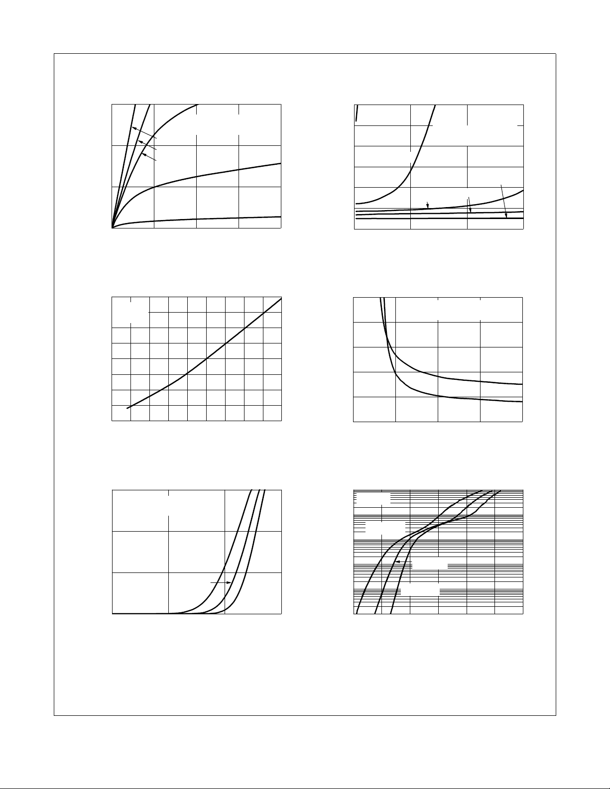
Typical Characteristics T
90
PULSE DURATION = 80 Ps
60
30
DRAIN CURRENT (A)
,
D
I
0
0.0 0.5 1.0 1.5 2.0
Figure 1.
VGS = 10 V
VGS = 4.5 V
VGS = 4 V
V
,
DRAIN TO SOURCE VOLTAGE (V)
DS
On-Region Characteristics Figure 2.
1.5
ID = 18 A
1.4
V
= 10 V
GS
1.3
1.2
1.1
1.0
NORMALIZED
0.9
0.8
DRAIN TO SOURCE ON-RESISTANCE
0.7
-75 -50 -25 0 25 50 75 100 125 150
T
,
JUNCTION TEMPERATURE
J
F i g u r e 3 . N o r m a l i z e d O n - R e s i s t a n c e
vs Junction Temperature
DUTY CYCLE = 0.5% MAX
= 25 °C unless otherwise noted
J
VGS = 3.5 V
VGS = 3 V
o
(
C
)
12
VGS = 3 V
10
8
VGS = 3.5 V
PULSE DURATION = 80 Ps
DUTY CYCLE = 0.5% MAX
6
NORMALIZED
4
VGS = 4 V
VGS = 4.5 V
VGS = 10 V
2
DRAIN TO SOURCE ON-RESISTANCE
0
0306090
I
,
DRAIN CURRENT (A)
D
N o r m a l i z e d O n - R e s i s t a n c e
vs Drain Current and Gate Voltage
12
)
:
(m
10
ID= 18 A
8
DRAIN TO
,
6
DS(on)
r
4
SOURCE ON-RESISTANCE
2
246810
V
,
GATE TO SOURCE VOLTAGE (V)
GS
PULSE DURATION = 80 Ps
DUTY CYCLE = 0.5% MAX
TJ= 125 oC
TJ= 25 oC
F i g u re 4 . O n - R e si s t a n c e v s G a t e t o
Source Voltage
®
SyncFET
TM
90
60
30
, DRAIN CURRENT (A)
D
I
0
FDMS0312S Rev.D
PULSE DURATION = 80 Ps
DUTY CYCLE = 0.5% MAX
V
= 5 V
DS
TJ = 125 oC
TJ = 25 oC
TJ = -55 oC
1234
VGS, GATE TO SOURCE VOLTAGE (V)
Figure 5. Transfer Characteristics
100
VGS= 0 V
10
TJ= 125 oC
1
0.1
0.01
, REVERSE DRAIN CURRENT (A)
S
I
0.001
0.0 0.2 0.4 0.6 0.8 1.0 1.2
VSD, BODY DI ODE FORWARD VOLTAGE (V)
Figure 6.
TJ = 25 oC
TJ = -55 oC
S o u r ce t o D r a i n Di o d e
Forward Voltage vs Source Current
www.fairchildsemi.com3
Page 4

FDMS0312S N-Channel PowerTrench
Typical Characteristics T
10
ID= 18 A
8
V
= 10 V
DD
6
4
2
, GATE TO SOURCE VOLTAGE (V)
GS
V
0
0 5 10 15 20 25 30 35
Qg, GATE CHARGE (nC)
Figure 7.
30
10
, AVALANCHE CURRENT (A)
AS
I
1
0.01 0.1 1 10 100
Gate Charge Characteristics Figure 8.
TJ= 25 oC
TJ= 125 oC
tAV, TIME IN AVALANCHE (ms)
Figure 9.
U n c l a m p e d I n d u c t i v e
Switching Capability
= 25 °C unless otherwise noted
J
VDD = 20 V
VDD = 15 V
TJ= 100 oC
3000
C
iss
1000
C
oss
CAPACITANCE (pF)
100
f = 1 MHz
V
= 0 V
GS
50
0.1 1 10 30
VDS, DRAIN TO SOURCE VOLTAGE (V)
C
rss
C a p a c i t a n c e v s D r a i n
to Source Voltage
90
60
VGS= 10 V
30
DRAIN CURRENT (A)
,
D
Limited by Packa ge
I
R
= 2.7 oC/W
T
JC
0
25 50 75 100 125 150
T
CASE TEMPERATURE
,
c
Figure 10.
M a x i m u m C o n t i n u o u s D r a i n
VGS= 4.5 V
o
C
(
)
Current vs Case Temperature
®
SyncFET
TM
300
100
10
1
, DRAIN CURRENT (A)
D
0.1
I
0.01
0.01 0.1 1 10 100200
FDMS0312S Rev.D
100 Ps
1 ms
THIS AREA IS
LIMITED BY r
DS(on)
SINGLE PULSE
= MAX RATED
T
J
= 125 oC/W
R
T
JA
T
= 25 oC
A
VDS, DRAIN to SOURCE VOLTAGE (V)
10 ms
100 ms
1 s
10 s
DC
F ig u re 1 1. F or w ar d B ia s Sa f e
Operating Area
3000
1000
VGS = 10 V
100
10
SINGLE PULSE
PEAK TRANSIENT POWER (W)
,
)
R
= 125 oC/W
T
0.5
JA
1
T
= 25 oC
A
PK
(
P
10-410-310-210
Figure 12.
Power Dissipation
-1
t, PULSE WIDTH (sec)
110
100 1000
S i n g l e P u l s e M a x i m u m
www.fairchildsemi.com4
Page 5

FDMS0312S N-Channel PowerTrench
Typical Characteristics T
2
1
DUTY CYCLE-DESCENDING ORDER
D = 0.5
0.2
0.1
0.05
0.02
0.01
SINGLE PULSE
R
JA
T
-4
10
-3
10
Figure 13. Junction-to-Ambient Transient Thermal Response Curve
NORMALIZED THERMAL
JA
T
Z
IMPEDANCE,
0.001
0.0001
0.1
0.01
= 25 °C unless otherwise noted
J
= 125 oC/W
-2
10
t, RECTANGULAR PULSE DURATION (sec)
-1
10
P
DM
NOTES:
DUTY FACTOR: D = t1/t
PEAK TJ = PDM x Z
TJA
110
t
1
t
2
2
x R
+ T
TJA
A
100 1000
®
SyncFET
TM
FDMS0312S Rev.D
www.fairchildsemi.com5
Page 6

Typical Characteristics (continued)
SyncFET Schottky body diode
Characteristics
Fairchild’s SyncFET process embeds a Schottky diode in parallel
with PowerTrench MoSFET. This diode exhibits similar
characteristics to a discrete external Schottky diode in parallel
with a MOSFET. Figure 14 shows the reverses recovery
characteristic of the FDMS0312S.
FDMS0312S N-Channel PowerTrench
Schottky barrier diodes exhibit significant leakage at high temperature and high reverse voltage. This will increase the power
in the device.
20
15
di/dt = 300 A/Ps
10
5
CURRENT (A)
0
-5
0306090120150
TIME (ns)
Figure 14. FDMS0312S SyncFET body
diode reverse recovery characteristic
-2
10
TJ= 125 oC
-3
10
-4
10
-5
10
, REVERSE LEAKAGE CURRENT (A)
-6
10
DSS
I
0 5 10 15 20 25 30
TJ= 100 oC
TJ= 25 oC
VDS, REVERSE VOLTAGE (V)
Figure 15. SyncFET body diode reverses
leakage versus drain-source voltage
®
SyncFET
TM
FDMS0312S Rev.D
www.fairchildsemi.com6
Page 7

Dimensional Outline and Pad Layout
FDMS0312S N-Channel PowerTrench
®
SyncFET
TM
FDMS0312S Rev.D
www.fairchildsemi.com7
Page 8

tm
®
tm
tm
™
TRADEMARKS
The following includes registered and unregistered tradema rks and service marks, owned by Fair child Semiconductor and/ or its global subsidiaries, and is no t
intended to be an exhaustive list of all such trademarks.
2Cool™
AccuPower™
Auto-SPM™
AX-CAP™*
®
BitSiC
Build it Now™
CorePLUS™
CorePOWER™
CROSSVOLT™
CTL™
Current Transfer Logic™
DEUXPEED
Dual Cool™
EcoSPARK
EfficentMax™
®
®
ESBC™
®
Fairchild
Fairchild Semiconductor
FACT Quiet Series™
®
FACT
®
FAST
FastvCore™
FETBench™
®
FlashWriter
FPS™
F-PFS™
FRFET
Global Power Resource
Green FPS™
Green FPS™ e-Series™
Gmax™
GTO™
IntelliMAX™
ISOPLANAR™
MegaBuck™
MICROCOUPLER™
MicroFET™
MicroPak™
MicroPak2™
MillerDrive™
MotionMax™
Motion-SPM™
mWSaver™
OptiHiT™
OPTOLOGIC
OPTOPLANAR
®
*
®
®
®
®
PDP SPM™
Power-SPM™
PowerTrench
PowerXS™
SM
Programmable Active Droop™
QFET
QS™
Quiet Series™
RapidConfigure™
®
®
Saving our world, 1mW/W/kW at a time™
SignalWise™
SmartMax™
SMART START™
®
SPM
STEALTH™
SuperFET
SuperSOT™-3
SuperSOT™-6
SuperSOT™-8
SupreMOS
SyncFET™
Sync-Lock™
®
®
®*
The Power Franchise
The Right Technology for Your Success™
TinyBoost™
TinyBuck™
TinyCalc™
TinyLogic
TINYOPTO™
TinyPower™
TinyPWM™
TinyWire™
TranSiC
TriFault Detect™
TRUECURRENT
μSerDes™
UHC
Ultra FRFET™
UniFET™
VCX™
VisualMax™
XS™
®
®
®
®
®
®
*
FDMS0312S N-Channel PowerTrench
®
SyncFET
TM
*Trademarks of System General Corporation, used under license by Fairchild Semiconductor.
DISCLAIMER
FAIRCHILD SEMICONDUCTOR RESERVES THE RIGHT TO MAKE CHANGES WITHOUT FURTHER NOTICE TO ANY PRODUCTS HEREIN TO IMPROVE
RELIABILITY, FUNCTION, OR DESIGN. FAIRCHILD DOES NOT ASSUME ANY LIABILITY ARISING OUT OF THE APPLICATION OR USE OF ANY
PRODUCT OR CIRCUIT DESCRIBED HEREIN; NEITHER DOES IT CONVEY ANY LICENSE UNDER ITS PATENT RIGHTS, NOR THE RIGHTS OF OTHERS.
THESE SPECIFICATIONS DO NOT EXPAND THE TERMS OF FAIRCHILD’S WORLDWIDE TERMS AND CONDITIONS, SPECIFICALLY THE WARRANTY
THEREIN, WHICH COVERS THESE PRODUCTS.
LIFE SUPPORT POLICY
FAIRCHILD’S PRODUCTS ARE NOT AUTHORIZED FOR USE AS CRITICAL COMPONENTS IN LIFE SUPPORT DEVICES OR SYSTEMS WITHOUT THE
EXPRESS WRITTEN APPROVAL OF FAIRCHILD SEMICONDUCTOR CORPORATION.
As used here in:
1. Life support devices or systems are devices or systems which, (a) are
intended for surgical implant into the body or (b ) support or su stain life,
and (c) whose failure to perform when properly used in acco rdance with
instructions for use provided in the labeling, can be reasonably
expected to result in a significant injury of the user.
ANTI-COUNTERFEITING POLICY
Fairchild Semiconductor Corporation’s Anti-Counterfeiting Policy. Fairchild’s Anti-Counterfeiting Policy is also stated on our external website,
www.Fairchildsemi.com, under Sales Support
Counterfeiting of semiconductor parts is a growing problem in the industry. All ma nufactures of semiconductor products are exper iencing counterfeiting of their
parts. Customers who inadvertently purchase counterfeit parts experience many proble ms su ch as loss of brand repu tation , substa ndard pe rfo rmance, f aile d
application, and increased cost of production and manufacturing delays. Fairchild is takin g stron g measures to protect ourselves and our customers from th e
proliferation of counterfeit parts. Fairchild str ongly encourages customers t o purchase Fairchild par ts either d irectly from Fairchild o r from Authorized Fairchild
Distributors who are listed by country on our web page cited above. Products customers buy either from Fairchild directly or from Authorized Fairchild
Distributors are genuine parts, have full traceability, meet Fairchild’s quality standards for handing and storage and provide access to Fairchild’s full range of
up-to-date technical and product information. Fairchild and our Authorized Distributors will stand behind all warranties and will appropriately address and
warranty issues that may arise. Fairchild will not provide any warranty coverage or other assistance for parts bought from Unauthorized Sources. Fairchild is
committed to combat this global problem and encourage our customers to do their part in stopping t his practice by buying direct or from authorized distributor s.
PRODUCT STATUS DEFINITIONS
Definition of Terms
.
2. A critical component in any component of a life support, device, or
system whose failure to perform can be reasonably expected to cause
the failure of the life support device or system, or to affect its safety or
effectiveness.
Datasheet Identification Product Status Definition
Advance Information Formative / In Design
Preliminary First Production
No Identification Needed Full Production
Obsolete Not In Production
FDMS0312S Rev.D
Datasheet contains the design specificatio ns for product development. Specifications
may change in any manner without notice.
Datasheet contains preliminary data; supplementary data will be published at a later
date. Fairchild Semiconductor reserves the right to make changes at any time without
notice to improve design.
Datasheet contains final specifications. Fairchild Semiconductor reserves the right to
make changes at any time without notice to improve the design.
Datasheet contains specifications on a product that is discontinu ed by Fai r child
Semiconductor. The datashe et is for reference information only.
Rev. I55
www.fairchildsemi.com8
 Loading...