

Page 1
November 1998
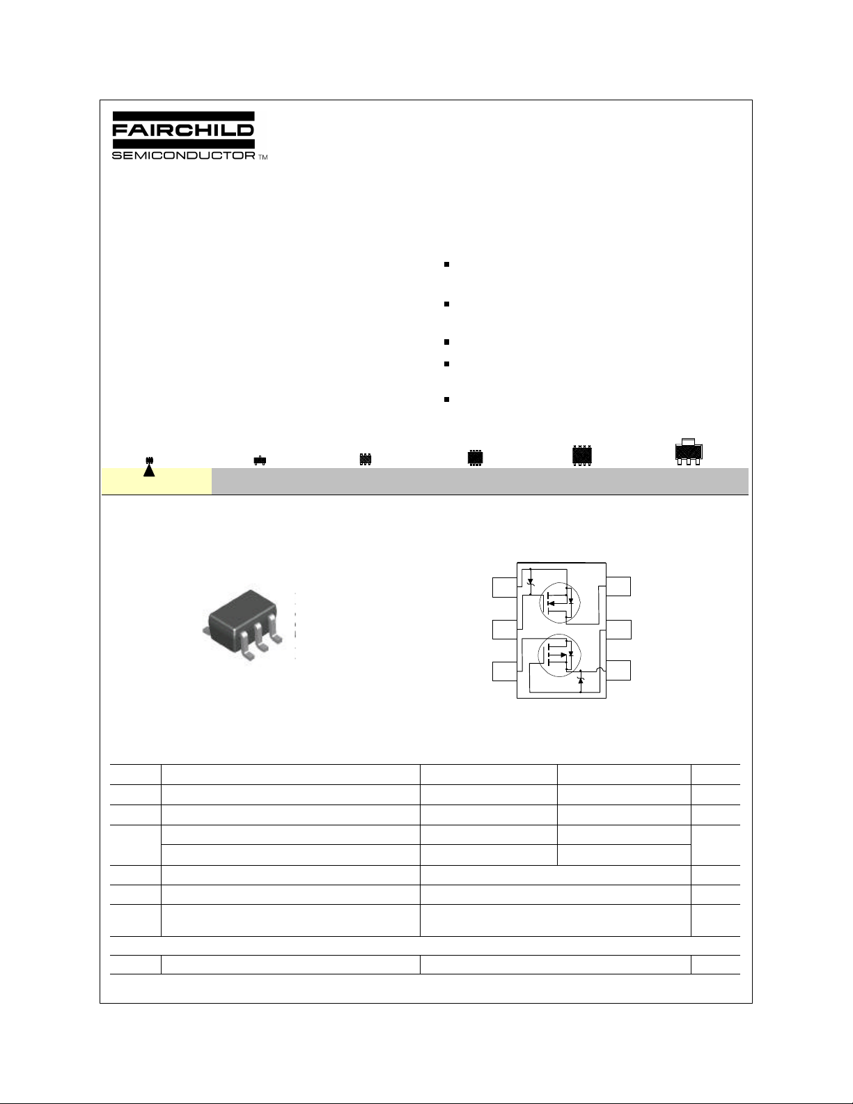
FDG6321C
Dual N & P Channel Digital FET
General Description Features
These dual N & P-Channel logic level enhancement mode field
effect transistors are produced using Fairchild's proprietary,
high cell density, DMOS technology. This very high density
process is especially tailored to minimize on-state resistance.
This device has been designed especially for low voltage
applications as a replacement for bipolar digital transistors and
small signal MOSFETS. Since bias resistors are not required,
this dual digital FET can replace several different digital
transistors, with different bias resistor values.
SC70-6
SOT-23
SuperSOTTM-6
S2
G2
D1
SC70-6
.21
S1
D2
G1
N-Ch 0.50 A, 25 V, R
R
P-Ch -0.41 A, -25 V,R
R
= 0.45 Ω @ VGS= 4.5V.
DS(ON)
= 0.60 Ω @ VGS= 2.7 V.
DS(ON)
= 1.1 Ω @ VGS= -4.5V.
DS(ON)
= 1.5 Ω @ VGS= -2.7V.
DS(ON)
Very small package outline SC70-6.
Very low level gate drive requirements allowing direct
operation in 3 V circuits(V
GS(th)
< 1.5 V).
Gate-Source Zener for ESD ruggedness
(>6kV Human Body Model).
SOT-8
1
2
3
SO-8
SOIC-14
6
5
4
Absolute Maximum Ratings T
= 25oC unless otherwise noted
A
Symbol Parameter N-Channel P-Channel Units
V
DS
V
GSS
I
D
Drain-Source Voltage 25 -25 V
S
Gate-Source Voltage 8 -8 V
Drain Current - Continuous 0.5 -0.41 A
- Pulsed 1.5 -1.2
P
D
TJ,T
ESD Electrostatic Discharge Rating MIL-STD-883D
Maximum Power Dissipation (Note 1) 0.3 W
Operating and Storage Temperature Ranger -55 to 150 °C
STG
6 kV
Human Body Model (100pf / 1500 Ohm)
THERMAL CHARACTERISTICS
R
θJA
© 1998 Fairchild Semiconductor Corporation
Thermal Resistance, Junction-to-Ambient (Note 1) 415 °C/W
FDG6321C Rev. D
Page 2
Electrical Characteristics (T
= 25 OC unless otherwise noted )
A
Symbol Parameter Conditions
OFF CHARACTERISTICS
BV
DSS
Drain-Source Breakdown Voltage VGS = 0 V, ID = 250 µA N-Ch 25 V
VGS = 0 V, ID = -250 µA
∆BV
DSS
Breakdown Voltage Temp. Coefficient ID= 250 µA, Referenced to 25 oC N-Ch 26 mV/oC
/∆T
J
ID = -250 µA, Referenced to 25 oC
I
DSS
I
GSS
I
GSS
Zero Gate Voltage Drain Current V
Gate - Body Leakage Current
Gate - Body Leakage Current
= 20 V, V
DS
VDS = -20 V, V
VGS = 8 V, V
VGS = -8 V, V
ON CHARACTERISTICS (Note 2)
V
GS(th)
Gate Threshold Voltage
VDS = VGS, ID = 250 µA
VDS = VGS, ID = -250 µA P-Ch -0.65 -0.82 -1.5
∆V
GS(th)
Gate Threshold Voltage Temp. Coefficient
/∆T
J
ID = 250 µA, Referenced to 25 oC
ID = -250 µA, Referenced to 25 oC P-Ch 2.1
R
DS(ON)
Static Drain-Source On-Resistance
VGS = 4.5 V, ID = 0.5 A
VGS = 2.7 V, ID = 0.2 A
VGS = -4.5 V, ID = -0.41 A P-Ch 0.85 1.1
VGS = -2.7 V, ID = -0.25 A 1.15 1.5
I
D(ON)
On-State Drain Current
VGS = 4.5 V, VDS = 5 V
VGS = -4.5 V, VDS = -5 V P-Ch -0.41
g
FS
Forward Transconductance
VDS = 5 V, ID = 0.5 A
VDS = -5 V, ID = -0.41 A P-Ch 0.9
DYNAMIC CHARACTERISTICS
C
iss
C
oss
Input Capacitance N-Channel N-Ch 50 pF
V
= 10 V, V
DS
Output Capacitance f = 1.0 MHz N-Ch 28
P-Channel P-Ch 34
C
rss
Reverse Transfer Capacitance
V
= -10 V, VGS = 0V,
DS
f = 1.0 MHz P-Ch 10
Min Typ Max Units
Type
P-Ch -25
P-Ch -22
= 0 V N-Ch 1 µA
GS
TJ = 55°C 10
GS
= 0 V
P-Ch -1 µA
TJ = 55°C -10
= 0 V
DS
= 0 V P-Ch -100 nA
DS
N-Ch 100 nA
N-Ch 0.65 0.8 1.5 V
N-Ch -2.6
N-Ch 0.34 0.45
TJ =125°C 0.55 0.72
0.44 0.6
TJ =125°C
1.2 1.8
N-Ch 0.5 A
N-Ch 1.45 S
GS
= 0 V,
P-Ch 62
N-Ch 9
mV/ oC
Ω
FDG6321C Rev. D
Page 3
Electrical Characteristics (continued)
SWITCHING CHARACTERISTICS (Note 2)
Symbol Parameter Conditions
t
D(on)
Turn - On Delay Time N-Channel N-Ch 3 6 nS
Type
VDD = 5 V, ID = 0.5 A, P-Ch 7 15
t
r
Turn - On Rise Time
V
= 4.5 V, R
GS
= 50 Ω
GEN
N-Ch 8.5 18 nS
P-Ch 8 16
t
D(off)
Turn - Off Delay Time P-Channel N-Ch 17 30 nS
VDD = -5 V, ID = -0.5 A, P-Ch 55 80
t
f
Turn - Off Fall Time
VGS = -4.5 V, R
GEN
= 50 Ω
N-Ch 13 25 nS
P-Ch 35 60
Q
g
Q
gs
Total Gate Charge N-Channel N-Ch 1.64 2.3 nC
V
= 5 V, ID = 0.5 A,
DS
P-Ch 1.1 1.5
Gate-Source Charge VGS = 4.5 V N-Ch 0.38 nC
P- Channel P-Ch 0.31
Q
gd
Gate-Drain Charge
VDS = -5 V, ID = -0.41 A,
VGS = -4.5 V
N-Ch 0.45 nC
P-Ch 0.29
DRAIN-SOURCE DIODE CHARACTERISTICS AND MAXIMUM RATINGS
I
S
Maximum Continuous Drain-Source Diode Forward Current N-Ch 0.25 A
P-Ch -0.25
V
SD
Notes:
1. R
design while R
2. Pulse Test: Pulse Width < 300µs, Duty Cycle < 2.0%.
Drain-Source Diode Forward Voltage VGS = 0 V, IS = 0.5 A
VGS = 0 V, IS = -0.5 A
is the sum of the junction-to-case and case-to-ambient thermal resistance where the case thermal reference is defined as the solder mounting surface of the drain pins. R
JA
θ
is determined by the user's board design. R
CA
θ
= 415OC/W on minimum mounting pad on FR-4 board in still air.
JA
θ
(Note 2) N-Ch 0.8 1.2 V
(Note 2)
P-Ch -0.85 -1.2
Min Typ Max Units
is guaranteed by
JC
θ
FDG6321C Rev. D
Page 4

Typical Electrical Characteristics: N-Channel
1.5
V = 4.5V
GS
3.0V
1.2
2.7V
0.9
0.6
0.3
D
I , DRAIN-SOURCE CURRENT (A)
0
0 0.5 1 1.5 2 2.5 3
2.5V
2.0V
1.5V
V , DRAIN-SOURCE VOLTAGE (V)
DS
Figure 1. On-Region Characteristics.
1.6
I = 0.5A
D
1.4
V = 4.5 V
GS
1.2
1
DS(ON)
R , NORMALIZED
0.8
DRAIN-SOURCE ON-RESISTANCE
0.6
-50 -25 0 25 50 75 100 125 150
T , JUNCTION TEMPERATURE (°C)
J
2
V = 2.0V
1.5
DS(ON)
R , NORMALIZED
DRAIN-SOURCE ON-RESISTANCE
0.5
GS
2.5V
2.7V
3.0V
1
0 0.2 0.4 0.6 0.8 1 1.2
I , DRAIN CURRENT (A)
D
3.5V
Figure 2. On-Resistance Variation with
Drain Current and Gate Voltage.
2
1.6
1.2
T = 125°C
0.8
0.4
DS(on)
R , ON-RESISTANCE (OHM)
0
1 1.5 2 2.5 3 3.5 4 4.5 5
V , GATE TO SOURCE VOLTAGE (V)
GS
A
T = 25°C
A
4.5V
I = 0.3A
D
Figure 3. On-Resistance Variation
with Temperature.
1
V = 5.0V
DS
0.8
0.6
0.4
D
I , DRAIN CURRENT (A)
0.2
0
0 0.5 1 1.5 2 2.5
V , GATE TO SOURCE VOLTAGE (V)
GS
Figure 5. Transfer Characteristics.
T = -55°C
J
25°C
125°C
Figure 4. On-Resistance Variation with
Gate-to-Source Voltage.
1
V = 0V
GS
T = 125°C
0.1
0.01
0.001
S
I , REVERSE DRAIN CURRENT (A)
0.0001
0 0.2 0.4 0.6 0.8 1 1.2
V , BODY DIODE FORWARD VOLTAGE (V)
SD
J
25°C
-55°C
Figure 6. Body Diode Forward Voltage
Variation with Source Current
and Temperature.
FDG6321C Rev. D
Page 5

Typical Electrical Characteristics: N-Channel (continued)
5
I = 0.5A
D
4
3
2
1
GS
V , GATE-SOURCE VOLTAGE (V)
0
0 0.4 0.8 1.2 1.6 2
Q , GATE CHARGE (nC)
g
V = 5V
DS
10V
15V
Figure 7. Gate Charge Characteristics.
3
1
0.5
RDS(ON) LIMIT
0.2
0.1
0.05
D
I , DRAIN CURRENT (A)
0.02
0.01
V = 4.5V
GS
SINGLE PULSE
JA
R = 415 °C/W
θ
T = 25°C
A
0.1 1 2 5 10 25 40
V , DRAI N-SOURCE VOLTAGE (V)
DS
10s
DC
10ms
100ms
1s
1ms
200
70
30
10
CAPACITANCE (pF)
f = 1 MHz
V = 0V
GS
3
0.1 0.3 1 2 5 10 25
V , DRAIN TO SOURCE VOLTAGE (V)
DS
C
C
C
iss
oss
rss
Figure 8. Capacitance Characteristics.
50
40
30
20
POWER (W)
10
0
0.0001 0.001 0.01 0.1 1 10 200
SINGLE PULSE TIME (SEC)
SINGLE PULSE
R =415°C/W
JA
θ
T = 25°C
A
Figure 9. Maximum Safe Operating Area.
Figure 10. Single Pulse Maximum Power
Dissipation.
FDG6321C Rev. D
Page 6

Typical Electrical Characteristics: P-Channel
1.2
V =-4.5V
0.9
0.6
0.3
D
-I , DRAIN-SOURCE CURRENT (A)
0
0 1 2 3 4
-3.0V
GS
-2.7V
-2.5V
-V , DRAIN-SOURCE VOLTAGE (V)
DS
-2.0V
Figure 11. On-Region Characteristics.
1.6
I = -0.41A
D
V = -4.5V
1.4
GS
1.2
1
DS(ON)
0.8
R , NORMALIZED
DRAIN-SOURCE ON-RESISTANCE
0.6
-50 -25 0 25 50 75 100 125 150
T , JUNCTION TEMPERATURE (°C)
J
-1.5V
2.5
V = -2.0V
2
GS
1.5
DS(ON)
1
R , NORMALIZED
DRAIN-SOURCE ON-RESISTANCE
0.5
0 0.2 0.4 0.6 0.8 1 1.2
-2.5V
-2.7V
-3.0V
-I , DRAIN CURRENT (A)
D
-3.5V
-4.5V
Figure 12. On-Resistance Variation with
Drain Current and Gate Voltage.
5
4
3
2
1
DS(ON)
R ,ON-RESISTANCE(OHM)
0
1 2 3 4 5
-V , GATE TO SOURCE VOLTAGE (V)
GS
I =-0.2A
D
T =125 °C
J
25°C
Figure 13. On-Resistance Variation
with Temperature.
1
V = -5V
DS
0.8
0.6
0.4
D
-I , DRAIN CURRENT (A)
0.2
0
0.5 1 1.5 2 2.5 3
-V , GATE TO SOURCE VOLTAGE (V)
GS
T = -55°C
J
25°C
125°C
Figure 15. Transfer Characteristics.
Figure 14. On-Resistance Variation with
Gate-to-Source Voltage.
1
V = 0V
GS
T = 125°C
0.1
J
25°C
0.01
0.001
S
-I , REVERSE DRAIN CURRENT (A)
0.0001
0.2 0.4 0.6 0.8 1 1.2
-V , BODY DIODE FORWARD VOLTAGE (V)
SD
-55°C
Figure 16. Body Diode Forward Voltage
Variation with Source Current
and Temperature.
FDG6321C Rev. D
Page 7

Typical Electrical Characteristics: P-Channel (continued)
5
I = -0.41A
D
4
3
2
1
GS
-V , GATE-SOURCE VOLTAGE (V)
0
0 0.4 0.8 1.2 1.6
3
1
0.5
RDS(ON) LIMIT
0.1
0.05
D
-I , DRAIN CURRENT (A)
0.01
V = -4.5V
SINGLE PULSE
R = 415°C
θ
A
T = 25°C
0.1 0.2 0.5 1 2 5 10 25 40
Q , GATE CHARGE (nC)
g
GS
JA
A
- V , DRAIN-SOURCE VOLTAGE (V)
DS
V = -5V
DS
10s
DC
-10V
-15V
100ms
1s
10ms
1ms
200
80
30
10
CAPACITANCE (pF)
f = 1 MHz
V = 0 V
5
GS
3
0.1 0.3 1 2 5 10 25
-V , DRAIN TO SOURCE VOLTAGE (V)
DS
C
iss
C
oss
C
rss
Figure 18. Capacitance Characteristics.Figure 17. Gate Charge Characteristics.
50
40
30
20
POWER (W)
10
0
0.0001 0.001 0.01 0.1 1 10 200
SINGLE PULSE TIME (SEC)
SINGLE PULSE
R =415°C/W
JA
θ
T = 25°C
A
Figure 19. Maximum Safe Operating Area.
Figure 20. Single Pulse Maximum Power
Dissipation.
FDG6321C Rev. D
Page 8

Typical Thermal Characteristics: N & P-Channel (continued)
1
D = 0.5
0.5
0.2
0.2
0.1
0.1
0.05
0.05
0.02
0.01
r(t), NORMALIZED EFFECTIVE
0.005
TRANSIENT THERMAL RESISTANCE
0.002
0.0001 0.001 0.01 0.1 1 10 100 200
0.02
0.01
Single Pulse
t , TIME (sec)
1
Figure 21. Transient Thermal Response Curve.
Thermal characterization performed using the conditions described in note 1.
Transient thermalresponse will change depending on the circuit board design.
R (t) = r(t) * R
JA
θ
R =415
JA
θ
P(pk)
t
1
t
2
T - T = P * R (t)
J
A
Duty Cycle, D = t / t
°C/W
JA
θ
1 2
JA
θ
FDG6321C Rev. D
Page 9

TRADEMARKS
The following are registered and unregistered trademarks Fairchild Semiconductor owns or is authorized to use and is
not intended to be an exhaustive list of all such trademarks.
ACEx™
CoolFET™
CROSSVOLT™
2
E
CMOS
TM
FACT™
FACT Quiet Series™
®
FAST
FASTr™
GTO™
HiSeC™
ISOPLANAR™
MICROWIRE™
POP™
PowerTrench™
QFET™
QS™
Quiet Series™
SuperSOT™-3
SuperSOT™-6
SuperSOT™-8
TinyLogic™
UHC™
VCX™
DISCLAIMER
FAIRCHILD SEMICONDUCTOR RESERVES THE RIGHT TO MAKE CHANGES WITHOUT FURTHER
NOTICE TO ANY PRODUCTS HEREIN TO IMPROVE RELIABILITY, FUNCTION OR DESIGN. FAIRCHILD
DOES NOT ASSUME ANY LIABILITY ARISING OUT OF THE APPLICA TION OR USE OF ANY PRODUCT
OR CIRCUIT DESCRIBED HEREIN; NEITHER DOES IT CONVEY ANY LICENSE UNDER ITS PATENT
RIGHTS, NOR THE RIGHTS OF OTHERS.
LIFE SUPPORT POLICY
FAIRCHILD’S PRODUCTS ARE NOT AUTHORIZED FOR USE AS CRITICAL COMPONENTS IN LIFE SUPPORT
DEVICES OR SYSTEMS WITHOUT THE EXPRESS WRITTEN APPROV AL OF FAIRCHILD SEMICONDUCTOR CORPORA TION.
As used herein:
1. Life support devices or systems are devices or
systems which, (a) are intended for surgical implant into
the body, or (b) support or sustain life, or (c) whose
failure to perform when properly used in accordance
with instructions for use provided in the labeling, can be
reasonably expected to result in significant injury to the
user.
2. A critical component is any component of a life
support device or system whose failure to perform can
be reasonably expected to cause the failure of the life
support device or system, or to affect its safety or
effectiveness.
PRODUCT STA TUS DEFINITIONS
Definition of Terms
Datasheet Identification Product Status Definition
Advance Information
Preliminary
No Identification Needed
Obsolete
Formative or
In Design
First Production
Full Production
Not In Production
This datasheet contains the design specifications for
product development. Specifications may change in
any manner without notice.
This datasheet contains preliminary data, and
supplementary data will be published at a later date.
Fairchild Semiconductor reserves the right to make
changes at any time without notice in order to improve
design.
This datasheet contains final specifications. Fairchild
Semiconductor reserves the right to make changes at
any time without notice in order to improve design.
This datasheet contains specifications on a product
that has been discontinued by Fairchild semiconductor.
The datasheet is printed for reference information only.
 Loading...