

Page 1
Philips Semiconductors Futurebus+ Products Preliminary specification
FB2012AFuturebus+ central arbitration controller
1
November 11, 1994
GENERAL DESCRIPTION OF THE FB2012A
The FB2012A is the central arbitration controller for the Futurebus+
product family. When a module needs to send data to or obtain data
from another module, it must first gain tenure of the bus. The
FB2012A controls or arbitrates tenure of the bus to one module at a
time.
The FB2012A includes BTL drivers and receivers for signals that
use the Futurebus+ backplane. Since the request and grant lines
are point-to-point, they need to be terminated only at the receiver.
Request lines are terminated at the FB2012A, and grant lines are
terminated at the individual Futurebus+ modules. If stub lengths to
the FB2012A create problems for the RE* and PE* signals, an
external BTL receiver may be used for RE* and and an external BTL
driver may be sourced by the TTL PE* signal. If the external BTL
receiver is inverting, the resulting TTL signal (RE*) must be inverted
as well.
GENERAL DESCRIPTION OF THE FUTUREBUS+ CENTRAL ARBITRATION PROTOCOL
A requesting module asserts either a level-1 (RQH*) or a level-0
(RQL*) request to obtain bus mastership. A low-priority (level-0)
request may become a high-priority request by leaving the
low-priority request asserted while also asserting the corresponding
high-priority (level-1) request.
A module may release the request(s) anytime after a grant is
received from the FB2012A if the need for a bus transaction
vanishes. Once a request is made, it may not be removed until the
corresponding grant has been received (according to IEEE 896.1).
(The FB2012A gives the user the option to release a request before
the corresponding grant is asserted or to follow IEEE 896.1.)
A requesting module becomes the bus master only after it receives
the bus grant and the current bus master releases its tenure (the
current bus master has released its request, but may still be in the
middle of a transaction). This condition is indicated by the continued
assertion of ET*. When the current bus master has finished its
transaction and has released the address/data bus, it releases ET*.
Once the module with the asserted bus grant detects the release of
ET*, it becomes the bus master and may begin its transaction. The
bus master’s request(s) must remain asserted until it asserts ET*.
Refer to FUNCTIONAL WAVEFORMS.
The central arbiter asserts PE* to indicate that a preemptive
condition exists and that the current bus master should relinquish
the bus. The definition of the preemptive condition is described in
the FUNCTIONAL DESCRIPTION section below.
FEATURES
•The Philips Semiconductors Central Arbitration Controller is
compatible with the IEEE P896.6 Futurebus+ standard
•14 level-1 first-come-first-served requests
•14 level-0 first-come-first-served requests
•14 bus grants
•Priority preemption
•Timing for Futurebus+ RE* signal
– Bus initialization
– System reset
•68-pin PLCC package
QUICK REFERENCE DATA
SYMBOL PARAMETER TYPICAL UNIT
t
PLH
Propagation delay 5.2
t
PHL
RQXn to GRn 8.6
ns
C
O
Output capacitance 6 pF
TTL outputs 4
I
OL
Output current
BTL outputs 80
mA
I
CC
Supply current 80 mA
ORDERING INFORMATION
PACKAGE
COMMERCIAL RANGE
V
CC
= 5V±10%; T
amb
= 0 to +70°C
DWG
No.
68-pin Plastic Leaded Chip Carrier FB2012AA 0398E
Page 2

Philips Semiconductors Futurebus+ Products Preliminary specification
FB2012AFuturebus+ central arbitration controller
November 11, 1994
2
PIN CONFIGURATION
6789
10
11
12
13
14
15
16
27 28 29 30 31 32 33
48
49
50
51
52
53
54
345
55
56
57
58
59
60
34 35 36 37 38 39
17
18
19
20
21
22
6812 656667
40 41 42 43
64 616263
44
45
46
47
23
24
25
26
RQL13*
pe
ANYGR*
BINIT*
SYSRST*
PPE*
BIAS V
V
CC
NC
LOGIC GND
EN*
TESTEN
TCK (option)
TMS (option)
TDO (option)
TDI (option)
RQH13*
GRO*
GR1*
GR2*
GR3*
BUS GND
GR4*
GR5*
GR6*
BUS GND
GR7*
GR8*
GR9*
BUS GND
GR10*
GR11*
GR12*
GR13*
RQL12*
RQL11*
RQL10*
RQL9*
RQL8*
Vcc
RQL7*
RQL6*
RQL5*
RQL4*
LOGIC GND
RQL3*
RQL2*
RQL1*
RQL0*
RE*
BUS GND
RQH12*
RQH11*
RQH10*
RQH9*
RQH8*
Vcc
RQH7*
RQH6*
RQH5*
RQH4*
LOGIC GND
RQH3*
RQH2*
RQH1*
RQH0*
PE*
BUS GND
Futurebus+ Central
Arbitration Controller
FB2012A
SG00054
LOGIC DIAGRAM
RQH[13-0]*(BTL)
RQL[13-0]*(BTL)
EN*
PPE*
RE*(BTL)
TESTEN
BIAS V
NC = 18
LOGIC GND(3)
BUS GND(5) (BTL)
V
CC
(3)
GR[13-0]* (BTL)
ANYGR*
PE* (BTL)
pe
BINIT*
SYSRST*
JTAG
(future boundary scan option)
TMS
TCK
TDI
TDO
26-31, 33-36,
38-41
1-3, 5-10,
63-66, 68
20
15
62
21
16
19, 37, 67
43, 48, 52, 56, 61
4, 17, 32
23
22
25
24
44-47, 49-51,
53-55,
57-60
12
42
11
13
14
CENTRAL
ARBITRATION
CONTROLLER
FB2012A
SG00055
Page 3

Philips Semiconductors Futurebus+ Products Preliminary specification
FB2012AFuturebus+ central arbitration controller
November 11, 1994
3
FUNCTIONAL DESCRIPTION OF THE FB2012A
The FB2012A has two priority levels, each with 14 inputs. For ease
of labeling, the two priority levels, labeled RQ1* and RQ0* in the
Futurebus+ 896.1 specification, are labeled RQHn* (level-1) and
RQLn* (level-0), respectively, on the FB2012A, where ‘n’ is the
module number from 0 through 13. The assignment of a module to
a particular request line has no significance; all requests (of a
particular priority level) are treated identically. Once asserted, a
request should remain asserted until the corresponding grant is
received (according to IEEE 896.1). (If the user chooses to release
a request before the corresponding grant is asserted, he may do so;
the FB2012A allows this option.) Level-0 and level-1 requests may
be asserted simultaneously. Refer to FUNCTIONAL WAVEFORMS
for general functionality.
A grant will become active only after any metastable conditions
involving its request(s) are resolved. Only one of the 14 grant lines
will be active at a time. The order of serviced requests for each
level is first-come-first-served (FCFS) — the request that has been
asserted the longest receives the grant. However, level-0 requests
are serviced only when no level-1 requests are asserted.
The grant outputs are enabled when the EN* input is Low. However,
when EN* is released while a grant is active, the grant will remain
active until the corresponding request(s) are released. Also,
whenever a grant is asserted, the ANYGR* output signal will also be
asserted.
The FB2012A has two preemption modes:
1. If the PPE* input is asserted (priority preemption mode), PE* and
pe will be asserted whenever there is a level-1 request that is not
being serviced while another grant is asserted. That is, the
preemption lines will be asserted if more than one level-1 request
is asserted or if a level-0 request is being serviced when a
level-1 request(s) is asserted.
2. If PPE* is not asserted, PE* and pe will be asserted whenever
two or more requests, regardless of their priority levels, are
asserted. (Assertion of a level-1 request and a level-0 request
from the same module is considered as a single request.)
The action taken by a module when PE* (and pe) are asserted is
strictly up to the designer.
The FB2012A monitors RE* to detect the signaling of the bus
initialize and system reset conditions. If the RE* input is asserted
less than 2.0ms, neither BINIT* (bus initialize) nor SYSRST*
(system reset) will be asserted. If RE* is asserted longer than
2.0ms, BINIT* may be asserted; and after 3.9ms BINIT* is
guaranteed to be asserted. If RE* is asserted longer than 30ms,
SYSRST* may be asserted; and after 60ms SYSRST* is also
guaranteed to be asserted. If asserted, BINIT* and SYSRST* will
be released after RE* has been released at least 60ns and no more
than 140ns.
When BINIT* is asserted, future grants are disabled in the same
way that they are disabled in response to the de-assertion of the
EN* signal. (Normally all requests are removed during bus
initialization). When SYSRST* is asserted, PE* (and pe) will also be
forced into the asserted state independently of pre-emption
conditions. After RE* has been continuously released for at least
1µs and for not more than 2.2µs, the grants are re-enabled and PE*
(with pe) is released from its forced assertion, if it had entered one.
(In some systems, the assertion of PE* for at least 1µs after the
release of RE* (following system reset) is a condition that signals
the presence of a central arbiter.)
To accommodate the possibility of a system requirement for
redundant and removable FB2012A, a BIAS V input is provided to
bias the internal BTL circuity. This way the redundant FB2012A may
be live inserted without disrupting system operation.
For designs with a single FB2012A, the BIAS V input should be
connected to V
CC
.
METASTABILITY CHARACTERISTICS OF THE FB2012A
One of the concerns when dealing with an asynchronous arbiter is
understanding what would happen when competing requests arrive
at the same time. Input requests are processed by a bank of
mutual-exclusion elements. A mutual-exclusion element (ME) is a
state-holding device that arbitrates between a pair of inputs. This is
the point at which metastabilities can occur. The design of the ME
precludes anomalous signaling by suppressing output assertion until
metastabilities are resolved.
To determine the Mean Time Between Unacceptable Delays
(MTBUD) the following formula is used:
MTBUD
exp(
t
)
(T
O
)(fr1fr2)
t’ is the maximum acceptable delay between the request edge
(RQXn) and the corresponding grant output signal (GR*); and f
rx
is
the frequency of the request inputs.
The central arbiter has metastability characteristics of τ of 93ps, T
O
of 2.3E33 seconds, and a normal propagation of 8.76ns measured
at room temperature and 5V V
CC
. (Those unfamiliar with these
parameters may consult Philips Semiconductors application note
AN219, “A Metastability Primer”.)
The following example shows that at an individual ME, metastability
induced delays of appreciable size are extremely rare.
Assume that there are two possible requests and the average
request frequency for each is 250kHz. From the formula above,
with a t’ of 10.76ns (8.76ns + 2ns), the MTBUD is calculated to be
341 hours. If t’ was 12.76ns, the MTBUD would be about 85 million
years. Notice that 12.76ns is only an additional four nanosecond
delay above the normal propagation delay. (This example assumes
that a module may make a request immediately upon releasing
tenure.)
The example illustrates only two modules competing for the bus. In
real systems more request channels are active and more MEs are
involved. If ‘n’ channels are active, then n(n-1)/2 MEs are active.
Note, however, that any metastabilities that occur while a grant is
active undesired delay would be noticed.
It is difficult to imagine that a user would ever experience a grant
delay that cannot be tolerated.
Page 4

Philips Semiconductors Futurebus+ Products Preliminary specification
FB2012AFuturebus+ central arbitration controller
November 11, 1994
4
PIN DESCRIPTION
SYMBOL TYPE PIN NUMBER FROM/TO FUNCTION
RQH[13-0]* I-BTL
26, 27, 28, 29, 30, 31, 33,
34, 35, 36, 38, 39, 40, 41
Futurebus+
These are level 1 requests. Grants are allocated on a
first-come-first-served (FCFS) basis. The request that has been asserted
the longest receives the grant.
RQL[13-0]* I-BTL
10, 9, 8, 7, 6, 5, 3, 2, 1,
68, 66, 65, 64, 63
Futurebus+
These are level 0 requests. Level 0 requests are serviced when no level
1 requests are asserted. Requests are serviced according to the order of
assertion (FCFS). The request that has been asserted the longest
receives the grant.
GR[13-0]* O-BTL
44, 45, 46, 47, 49, 50, 51,
53, 54, 55, 57, 58, 59, 60
Futurebus+
Each GRn* corresponds to an RQHn* and RQLn*. Once asserted a
request must remain asserted until its corresponding grant is asserted. A
grant GRn* is de-asserted when both the corresponding RQHn* and
RQLn* are de-asserted. (Open-collector)
ANYGR* O-TTL 12 Module If any GR* pin is asserted ANYGR* is also asserted.
BINIT* O-TTL 13 Module
Signals other controllers to initialize their Futurebus+ signals. This pin is
driven Low after RE* is Low has been asserted for more than 2.0ms. Will
return High after RE* has been released for at least 60ms.
EN* I-TTL 20 Module
When high, all GR* lines that are not asserted will remain not asserted.
An asserted GRn* will remain asserted until both the associated RQHn*
line and RQLn* line are released.
pe O-TTL 11 Futurebus+ pe is the inverted TTL equivalent of the BTL PE* pin.
PE* O-BTL 42 Futurebus+
When PPE* is Low, PE* will be asserted whenever there is a level-1
request that is not being serviced while another grant is asserted. When
PPE* is High, PE* will be asserted if more than one request (level-1
PPE* I-TTL 15 Module
and/or level-0) is asserted. If level-1 and level-0 requests from the same
module (i.e., RQH1 and RQL1), they are considered as one request.
(PE* is Open-collector)
RE* I-BTL 62 Futurebus+ Futurebus+ reset.
SYSRST* O-TTL 14 Module
Indicates a system reset has been signaled on the Futurebus.
(Open-collector)
TESTEN I-TTL 21 Tester Used only for out-of-board testing (users should hold this pin low).
BIAS V I-TTL 16
Low current input to properly bias the BTL drivers during live insertion or
withdrawal. If live insertion or withdrawal is not a design consideration,
this pin should be connected to V
CC
.
LOGIC
GND
G-TTL 19, 37, 67 TTL ground.
BUS GND G-BTL 43, 48, 52, 56, 61 BTL ground.
V
CC
V 4, 17, 32 Power supply.
JTAG[TDI,
TDO, TMS,
TCK]
I/O-TTL 25, 24, 23, 22 Module
These four pins are reserved for future implementation of the JTAG
standard. TDI and TDO are shorted together. TMS and TCK are not
connected.
NC NC 18 No connect (reserved for future use).
Page 5
Philips Semiconductors Futurebus+ Products Preliminary specification
FB2012AFuturebus+ central arbitration controller
November 11, 1994
5
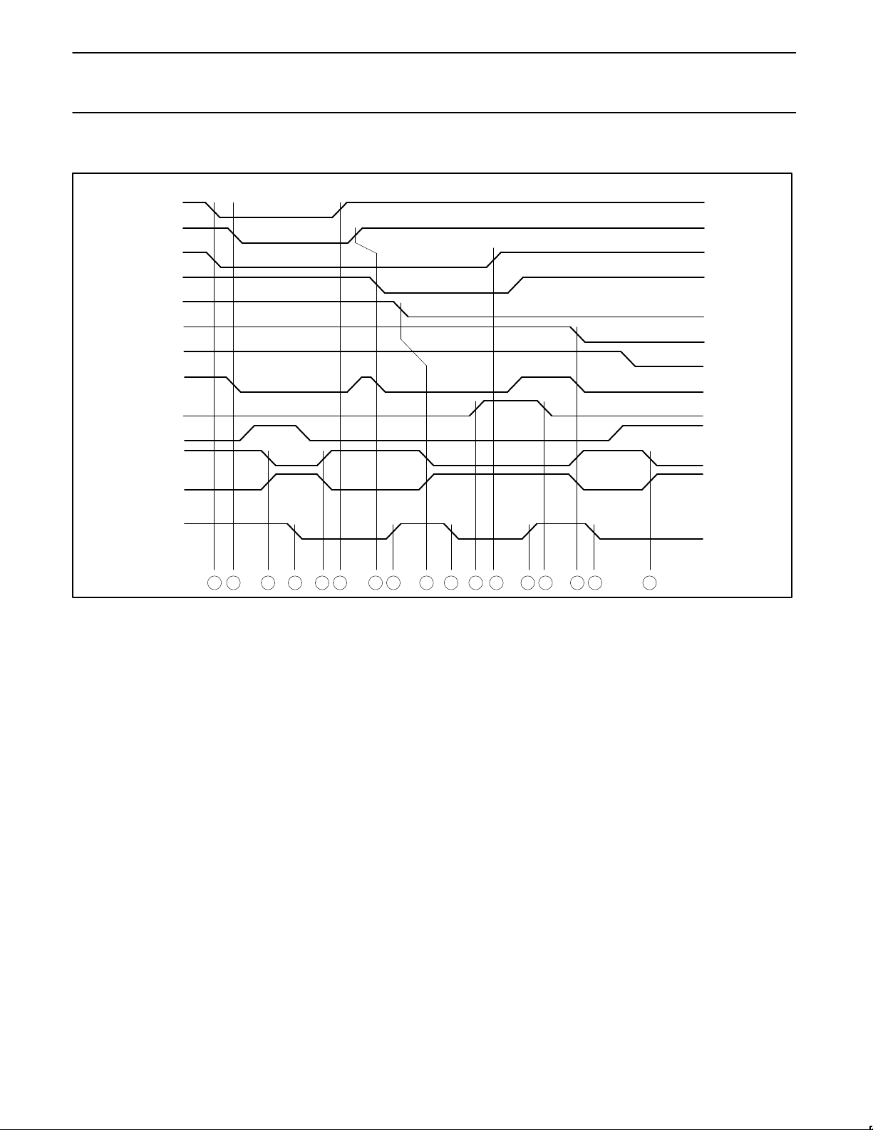
FUNCTIONAL WAVEFORMS
1
SIGNALS
2 3 4 5 6 7 8 9 10 11 12 13 14 15 16 17
RQH0*
GR0*
RQL1*
GR1*
RQH2*
GR2*
RQH3*
ANYGR*
EN*
PPE*
PE*
pe
FBUS+ SIGNAL
ET*
SG00051
1. Module 0 and module 1 make request (RQH0 and RQL1) ––
grant given to module 0 due to level-1 priority request.
2. Central Arbitration Controller asserts GR0* and ANYGR*.
3. The preemption outputs (PE* and pe) are asserted indicating
that multiple modules are requesting grants.
4. The current bus master, module 0, asserts et* after beginning a
transaction.
5. The priority preemption input (PPE*) has gone low which causes
the preemption outputs (PE* and pe) to be released.
6. Module 0 finishes its need for bus tenure and releases its
request.
7. The Central Arbitration Controller detects the release of the
module 0 request and releases the corresponding grant. The
Module 1 request is then serviced –– GR1* is asserted (and
ANYGR* also). Module 1 is now the bus master elect.
8. The bus master (module 0) releases et* to indicate to module 1
that it, module 1, is the new bus master.
9. A new level-1 request is received from module 2. Since PPE* is
asserted it causes PE* and pe to be asserted indicating that
there is an unserviced level-1 request.
10.Module 1 asserts et* after beginning a transaction.
11.The EN* pin is released blocking service to any unserviced
requests. The asserted grant (GR1*) remains asserted until the
corresponding requests are released.
12.Module 1 releases its request. Because EN* is High no new
grants are asserted.
13.Module 1 releases et*.
14.EN* is again asserted.
15.The module 2 grant (GR2*) becomes asserted. PE* and pe are
released because the level-1 request is now serviced.
16.Module 2, now the bus master, asserts et* after beginning a
transaction.
17.When module 3 asserts its request, PE* and pe become
asserted because now two requests are asserted at the same
time (and PPE* is High).
Page 6
Philips Semiconductors Futurebus+ Products Preliminary specification
FB2012AFuturebus+ central arbitration controller
November 11, 1994
6
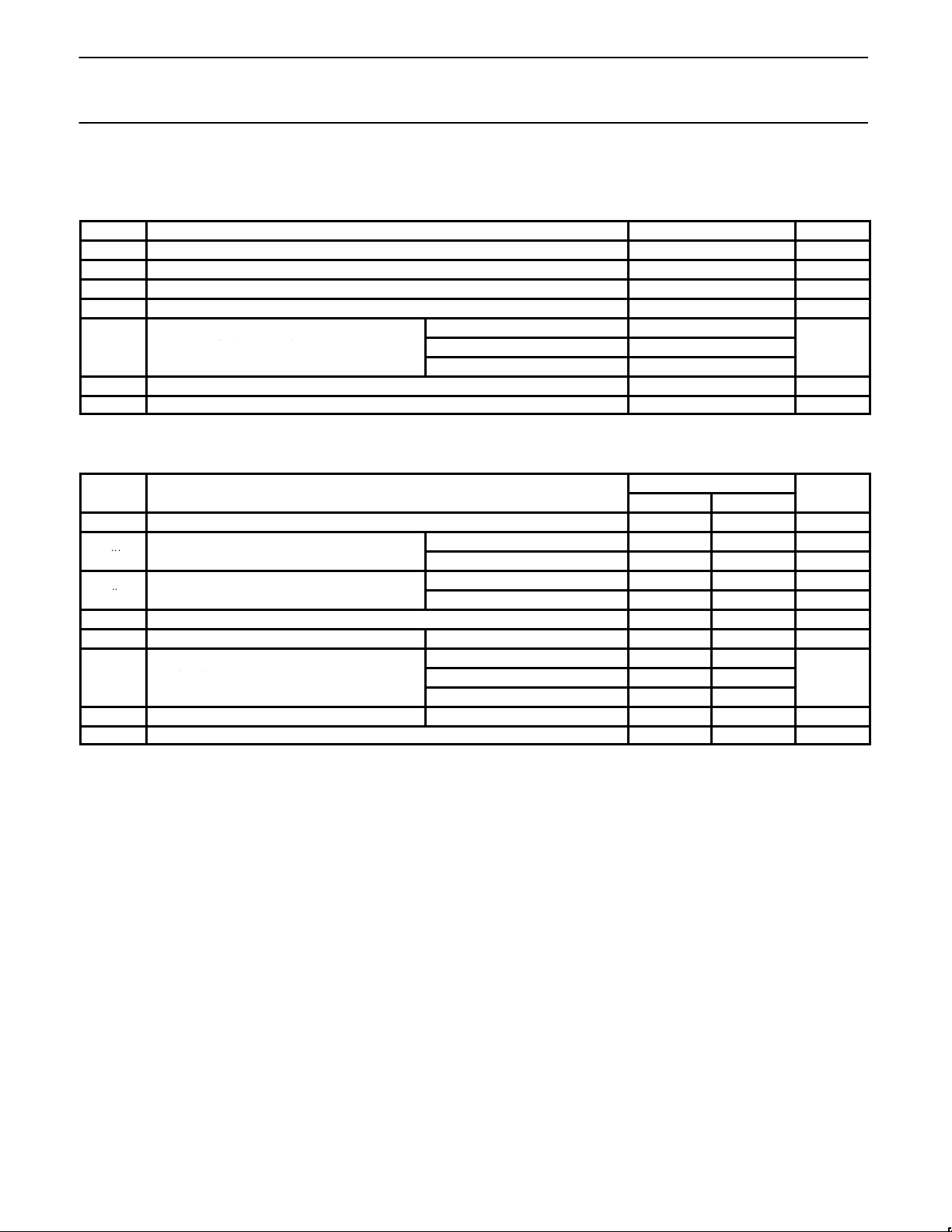
ABSOLUTE MAXIMUM RATINGS
Operation beyond the limits set forth in this table may impair the useful life of the device. Unless otherwise noted, these limits are over the
operating free-air temperature range.
SYMBOL
PARAMETER RATING UNIT
V
CC
Supply voltage -0.5 to +7.0 V
V
IN
Input voltage -1.2 to +7.0 V
I
IN
Input current -18 to +5 mA
V
OUT
Voltage applied to output in High output state -0.5 to +V
CC
V
TTL outputs except SYSRST* 8
SYSRST* 24
OUT
GR0* - GR13, PE* 80
T
amb
Operating free-air temperature range 0 to +70 °C
T
STG
Storage range -65 to +150 °C
RECOMMENDED OPERATING CONDITIONS
LIMITS
SYMBOL
PARAMETER
Min Max
UNIT
V
CC
DC supply voltage 4.5 5.5 V
TTL inputs 2.0 V
VIHHigh-level input voltage
RQX0* - RQX13*, RE* 1.62 V
TTL inputs 0.8 V
VILLow-level input voltage
RQX0* - RQX13*, RE* 1.47 V
I
IK
Input diode current -18 mA
I
OH
High level output current TTL except SYSRST* -1 mA
TTL except SYSRST* 4
SYSRST* 24
OL
GR0* - GR13, PE* 80
C
O
Output capacitance GRn*, PE* 7 pF
T
amb
Operating free-air temperature range 0 +70 °C
I
OUT
Current applied to output in Low output state
I
Low-level output current
OL
mA
mA
Page 7
Philips Semiconductors Futurebus+ Products Preliminary specification
FB2012AFuturebus+ central arbitration controller
November 11, 1994
7
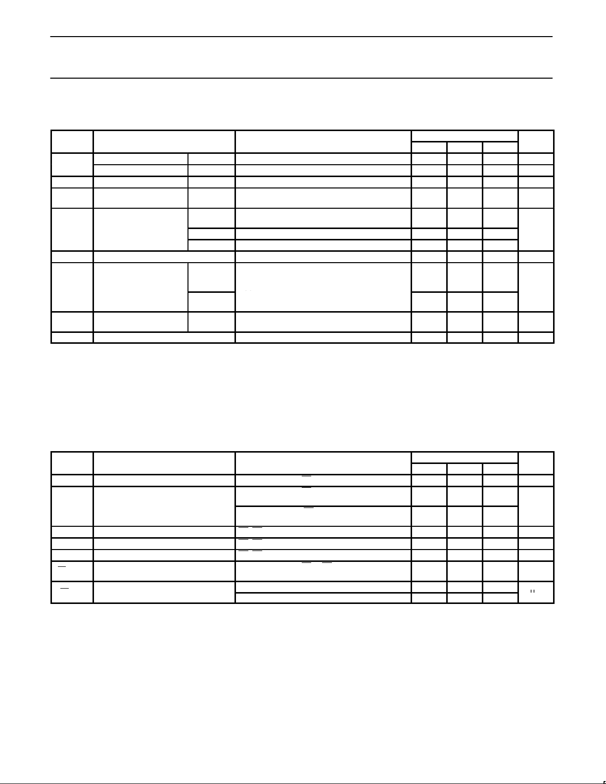
DC ELECTRICAL CHARACTERISTICS
Over recommended operating free-air temperature range unless otherwise noted.
1
LIMITS
SYMBOL
PARAMETER
TEST CONDITIONS
1
MIN TYP
2
MAX
UNIT
I
OH
High level output current SYSRST* VCC = MAX, VIL = MAX, VIH = MIN, VOH = 4.5V 100 µA
High level output current GRn*, PE* VCC = MAX, VIL = MAX, VIH = MIN, VOH = 2.1V 100 µA
I
OFF
Power-off output current GRn*, PE* VCC = 0.0V, VIL = MAX, VIH = MIN, VOH = 2.1V 100 µA
V
OH
High level output voltage
ANYGR*,
BINIT, pe
4
VCC = MIN, VIL = MAX, VIH = MIN, IOH = –1mA 2.5 2.85 V
ANYGR*,
BINIT, pe
4
VCC = MIN, VIL = MAX, VIH = MIN, IOL = 4mA 0.33 0.5
VOLLow level output voltage
SYSRST* VCC = MIN, VIL = MAX, VIH = MIN, IOL = 24mA 0.33 0.5
V
GRn*, PE* VCC = MIN, VIL = MAX, VIH = MIN, IOL = 80mA .75 1.0 1.10
V
IK
Input clamp voltage VCC = MIN, II = I
IK
–1.2 V
EN*,
PPE*,
TESTEN
±50
µA
I
I
maximum input voltage
RQXn*,
RE*
VCC = MAX, VI = GND or 5.5V
±100
µA
I
OS
Short circuit output
current
3
ANYGR*,
BINIT, pe
VCC = MAX, VO = 0V –30 –100 mA
I
CC
Supply current (total) VCC = MAX, Outputs High or Low 80 120 mA
NOTES:
1. For conditions shown as MIN or MAX, use the appropriate value specified under recommended conditions for the applicable type.
2. All typical values are at V
CC
= 5V, TA = 25°C.
3. Not more than one output should be shorted at a time. For testing I
OS
, the use of high-speed test apparatus and/or sample-and-hold
techniques are preferable in order to minimize internal heating and more accurately reflect operational values. Otherwise, prolonged
shorting of a High output may raise the chip temperature well above and thereby cause invalid readings in other parameter tests. In any
sequence of parameter test, I
OS
tests should be performed last.
4. Due to test equipment limitations, actual test conditions are VIH = 1.8V and VIL = 1.3V for BTL inputs.
LIVE INSERTION SPECIFICATIONS
1
LIMITS
SYMBOL
PARAMETER
TEST CONDITIONS
1
MIN TYP
2
MAX
UNIT
V
BIASV
Bias pin voltage VCC = 0 to 5.25V, Bn = 0 to 2.0V 4.5 5.5 V
VCC = 0 to 4.75V, Bn = 0 to 2.0V,
Bias V = 4.5 to 5.5V
1
I
BIASV
Bias pin DC current
VCC = 4.5 to 5.5V, Bn = 0 to 2.0V,
Bias V = 4.5 to 5.5V
10
mA
VBn Bus voltage during prebias B0–B8 = 0V, Bias V = 5.0V 1.62 1.9 2.1 V
I
LM
Fall current during prebias B0–B8 = 2V, Bias V = 4.5 to 5.5V 1 µA
I
HM
Rise current during prebias B0–B8 = 1V, Bias V = 4.5 to 5.5V -1 µA
IBnPEAK Peak bus current during insertion
VCC = 0 to 5.25V, B0 to B8= 0 to 2.0V,
Bias V = 4.5 to 5.5V, OEB0 = 0.8V, t
r
= 2ns
10 mA
VCC = 0 to 5.25V, OEB0 = 0.8V 100
IOLOFF
Power up current
VCC = 0 to 2.2V, OEB0 = 0 to 5V 100
µA
I
I
Input current at
VCC = MAX, VI = GND or 5.5V
Page 8
Philips Semiconductors Futurebus+ Products Preliminary specification
FB2012AFuturebus+ central arbitration controller
November 11, 1994
8
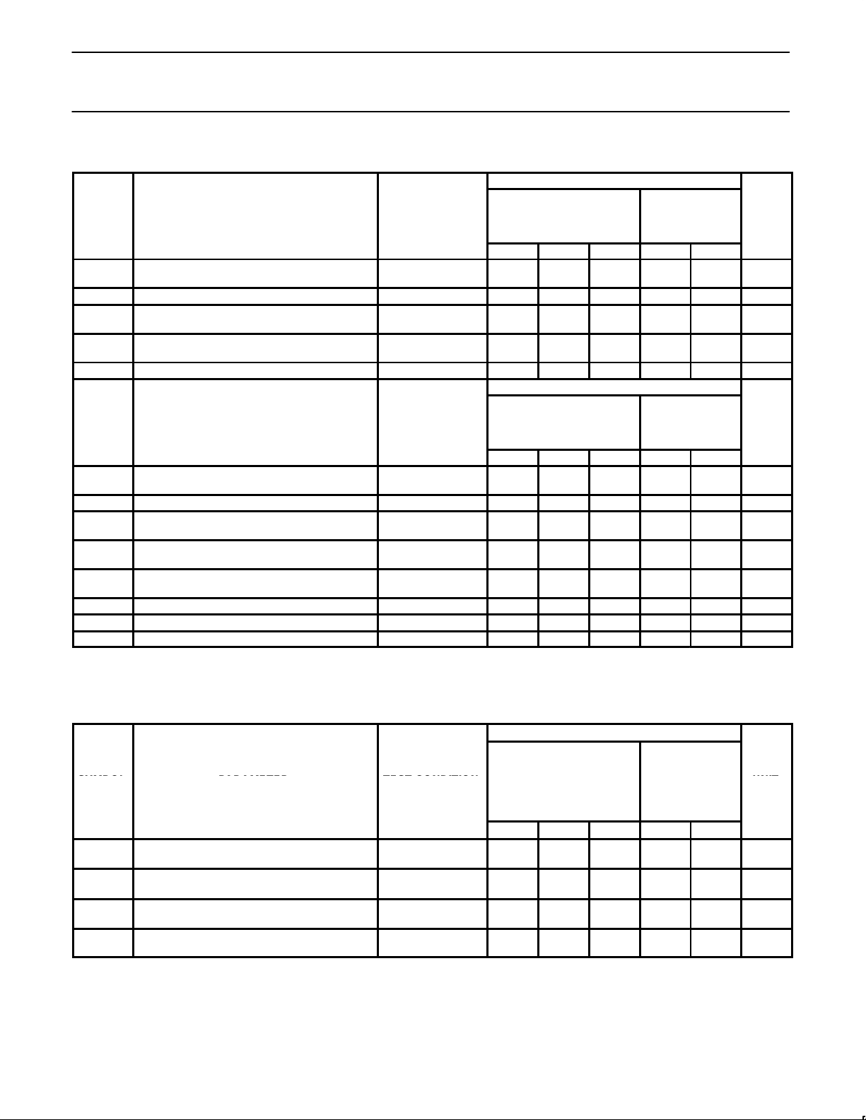
AC ELECTRICAL CHARACTERISTICS
TTL LIMITS
SYMBOL
PARAMETER
TEST CONDITION
T
amb
= +25°C
V
CC
= 5V
C
L
= 50pF
R
L
= 500Ω
T
amb
= 0 - +70°C
V
CC
= 5V ±10%
C
L
= 50pF
R
L
= 500Ω
UNIT
MIN TYP MAX MIN MAX
t
PLH
t
PHL
Propagation delay RQHn* or RQLn* to pe
(PPE* = High)
Waveform 2
8.5
8.0
10.5
10.0
12.0
12.5
7.5
7.0
14.0
14.0
ns
t
PLH
Propagation delay RQHn* to pe (PPE* = Low) Waveform 2 8.0 9.7 11.0 6.5 14.0 ns
t
PHL
Propagation delay RQHa* to pe
(PPE* = Low)
1
Waveform 2 7.5 9.0 10.5 6.5 11.5 ns
t
PLH
t
PHL
Propagation delay RQHn* or RQLn* to
ANYGR*
Waveform 1
7.5
8.5
9.5
10.9
11.0
13.0
6.5
7.5
12.5
15.0
ns
t
PHL
Propagation delay EN* to ANYGR* Waveform 1 8.0 9.5 11.0 7.0 12.5 ns
BTL LIMITS
SYMBOL
PARAMETER
TEST
CONDITIONS
T
amb
= +25°C
V
CC
= 5V
C
D
= 30pF
R
U
= 16.5Ω
T
amb
= 0 - +70°C
V
CC
= 5V ±10%
C
D
= 30pF
R
U
= 16.5Ω
UNIT
MIN TYP MAX MIN MAX
t
PLH
t
PHL
Propagation delay RQHn* or RQLn* to GRn* Waveform 1
2.0
6.5
5.2
8.6
7.0
11.5
2.0
6.0
7.5
12.5
ns
t
PHL
Propagation delay RQHa* or RQLa* to GRb*
1
Waveform 2 10.0 12.0 14.0 9.0 15.5 ns
t
PLH
t
PHL
Propagation delay RQHn* or RQLn* to PE*
(PPE* = High)
Waveform 1
7.5
7.5
9.3
9.2
12.5
11.0
6.5
6.5
14.0
12.5
ns
t
PHL
Propagation delay RQHn* to PE*
(PPE* = Low)
Waveform 1 6.5 8.0 9.5 5.5 12.0 ns
t
PLH
Propagation delay RQHa* to PE*
(PPE* = Low)
1
Waveform 1 7.0 8.3 10.0 6.5 11.5 ns
t
PHL
Propagation delay EN* to GRn* Waveform 1 6.0 7.3 9.0 5.5 9.5 ns
t
TLH
Rise time BTL outputs Waveform 3 0.8 0.8 ns
t
THL
Fall time BTL outputs Waveform 3 0.6 0.6 ns
NOTE:
1. RQHa or RQLa represent requests that already have a corresponding GRa* grant asserted. GRb* represents a grant not yet asserted, but
GRb* becomes asserted when GRa* is released, if RQHb and/or RQLb are asserted.
AC SETUP REQUIREMENTS
SETUP LIMITS
SYMBOL
PARAMETER
TEST CONDITION
T
amb
= +25°C
V
CC
= 5V
C
D
= 30pF
R
U
= 16.5Ω
C
L
= 50pF
R
L
= 500Ω
T
amb
= 0 - +70°C
V
CC
= 5V ±10%
C
D
= 30pF
R
U
= 16.5Ω
C
L
= 50pF
R
L
= 500Ω
UNIT
MIN TYP MAX MIN MAX
tW(L)
RE* pulse width, Low
(to assert BINIT*)
2.0 3.9 2.0 3.9 ms
tW(L)
RE* pulse width, Low
(to assert SYSRST*)
30.0 60 30.0 60 ms
t
rec
Recovery time
RE* to BINIT* or SYSRST*
60.0 100 140 60.0 140 ns
t
rec
Recovery time
RE* to GRn*
1.0 2.2 1.0 2.2 µs
Page 9
Philips Semiconductors Futurebus+ Products Preliminary specification
FB2012AFuturebus+ central arbitration controller
November 11, 1994
9
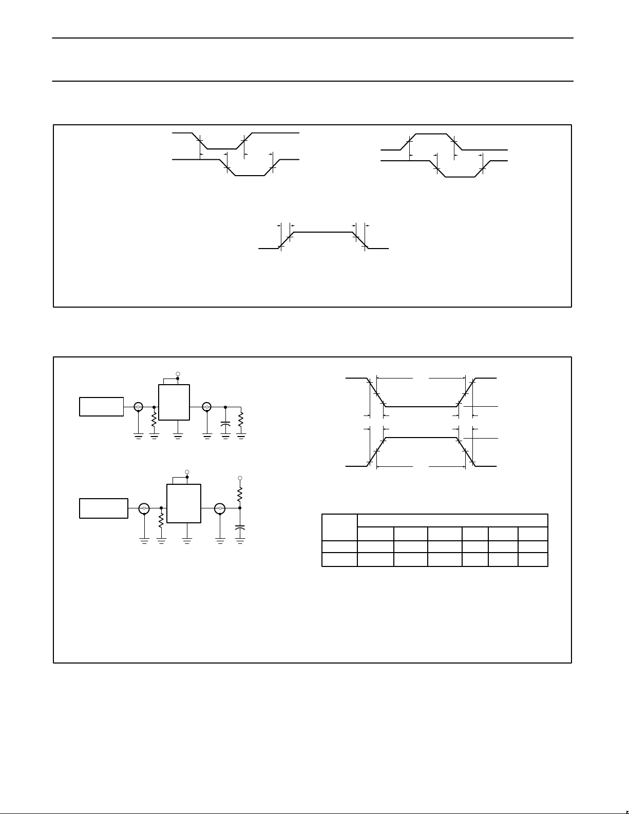
AC WAVEFORMS
RQHn*, RQLn*,
PPE*, EN*
GRn*, ANYGR*,
PE*, pe
V
M
t
PHL
t
PLH
RQHa*, RQLa*,
PE*, pe, GRb*
RQHn*, RQLn*,
PPE*, EN*
V
M
V
M
V
M
V
M
V
M
V
M
V
M
t
PHL
t
PLH
Waveform 1. Propagation Delay For
Non-Inverting Paths
Waveform 2. Propagation Delay For
Inverting Paths
NOTE: V
M
= 1.55V for RQHn*, RQLn*, RQHa*, RQLa*, GRn*, GRb* or PE*, VM = 1.5V for all others.
The Shaded areas indicate when the inputs is permitted to change for predictable output performance.
SG00052
1.3V
1.8V
1.3V
t
TLH
t
THL
1.8V
Waveform 3. Rise and Fall Time BTL Outputs
TEST CIRCUIT AND WAVEFORMS
PULSE
GENERATOR
D.U.T.
Test Circuit For Outputs On TTL Port
V
IN
V
OUT
R
L
C
L
R
T
V
CC
PULSE
GENERATOR
D.U.T.
V
IN
V
OUT
R
U
R
T
V
CC
C
D
Test Circuit For Outputs On BTL Port
FAMILY
FB+
TTL Port
BTL Port
INPUT PULSE REQUIREMENTS
Amplitude Low V Rep Rate
t
WtTLHtTHL
3.0V
2.0V
0.0V
1.0V
1MHz
1MHz
500ns
500ns
2.5ns
2.5ns
2.5ns
2.5ns
NEGATIVE
PULSE
POSITIVE
PULSE
10%
90%
AMP (V)
LOW V
AMP (V)
LOW V
V
M
V
M
V
M
V
M
V
M
10%
10% 10%
90%
90% 90%
t
W
t
W
t
THL
(tf)
t
TLH
(tr)
t
THL
(tf)
t
TLH
(tr)
V
M
= 1.55V for RQHn*, RQLn* or RE*,
V
M
= 1.5V for all others
Input Pulse Definition
DEFINITIONS
R
L
= Load resistor; see AC CHARACTERISTICS for value.
C
L
= Load capacitance includes jig and probe capacitance;
see AC CHARACTERISTICS for value.
R
T
= Termination resistance should be equal to Z
OUT
of
pulse generators.
C
D
= Load capacitance includes jig and probe capacitance;
see AC CHARACTERISTICS for value.
R
U
= Pull up resistor; see AC CHARACTERISTICS for value.
SG00053
 Loading...